


SPECIAL TOPIC—2D materials and future information devices

EDITOR'S SUGGESTION
2025, 74 (22): 226401.
doi: 10.7498/aps.74.20251141
Abstract +
EDITOR'S SUGGESTION
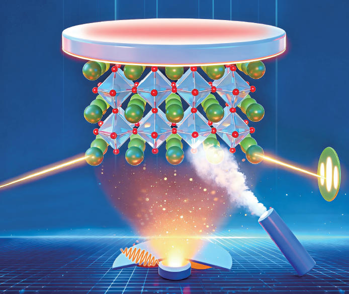
2025, 74 (22): 227501.
doi: 10.7498/aps.74.20251177
Abstract +
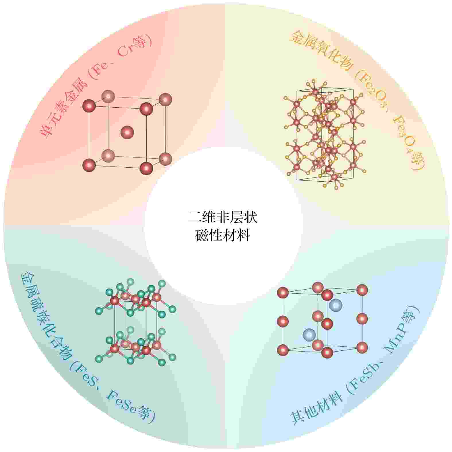
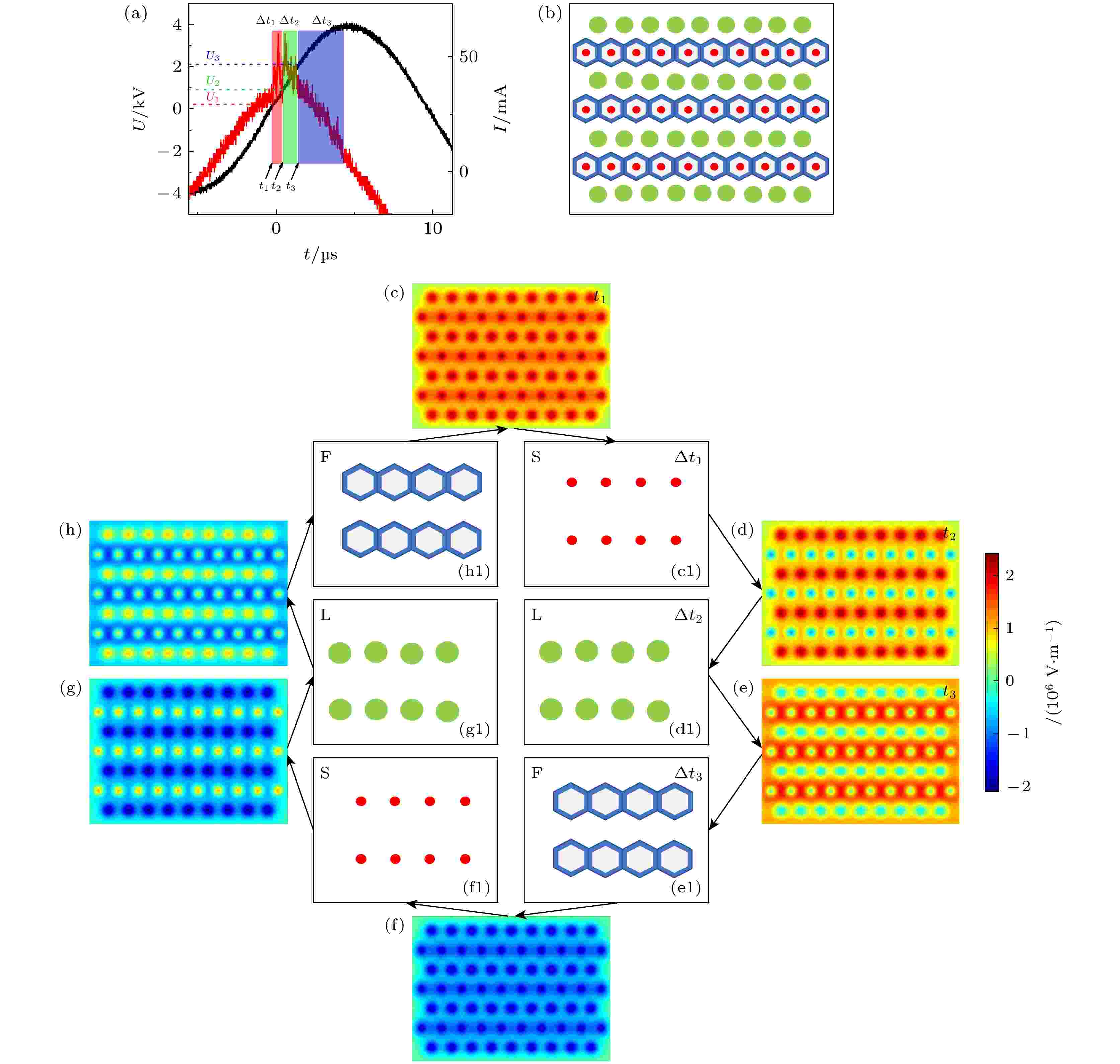
Two-dimensional (2D) magnetic materials refer to nanomaterials with an extremely thin thickness that can maintain long-range magnetic order. These materials exhibit significant magnetic anisotropy, and due to the quantum confinement effect and high specific surface area, their electronic band structures and surface states undergo remarkable changes. As a result, they possess rich and tunable magnetic properties, showing great application potential in the field of spintronics. The 2D magnetic materials include layered materials, where layers are stacked by weak van der Waals forces, and non-layered materials, which are bonded via chemical bonds in all three-dimensional directions. Currently, most of researches focus on 2D layered materials, but their Curie temperatures are generally much lower than room temperature, and they are always unstable when exposed to air. In contrast, the non-layered structure enhances the structural stability of the materials, and the abundant surface dangling bonds increase the possibility of modifying their physical properties. Such materials are attracting increasing attention, and significant progress has been made in their synthesis and applications. This review first systematically summarizes various preparation methods for 2D non-layered magnetic materials, including but not limited to ultrasound-assisted exfoliation, molecular beam epitaxy, and chemical vapor deposition. Meanwhile, it systematically reviews the 2D non-layered intrinsic magnetic materials obtained in various types of materials in the past five years, as well as a series of novel physical phenomena emerging under the ultrathin limit, such as thickness-dependent magnetic reconstruction dominated by quantum confinement effects and planar topological spin textures induced by 2D structures. Furthermore, it also discusses the critical role played by theoretical calculations in predicting new materials through high-throughput screening, revealing microscopic mechanisms by analyzing magnetic interactions, as well as some important methods of modifying magnetism. Finally, from the perspectives of material preparation, physical mechanisms, device fabrication, and theoretical calculations, the current challenges in the field are summarized, and the application potential and development directions of 2D non-layered magnetic materials in spintronic devices are prospected. This review aims to provide comprehensive references and scientific perspective for researchers engaged in this field, thereby promoting further exploration of the novel magnetic properties of 2D non-layered magnetic materials and their applications in spintronic devices.
EDITOR'S SUGGESTION
2025, 74 (22): 228101.
doi: 10.7498/aps.74.20251305
Abstract +
EDITOR'S SUGGESTION
2025, 74 (22): 228501.
doi: 10.7498/aps.74.20251093
Abstract +
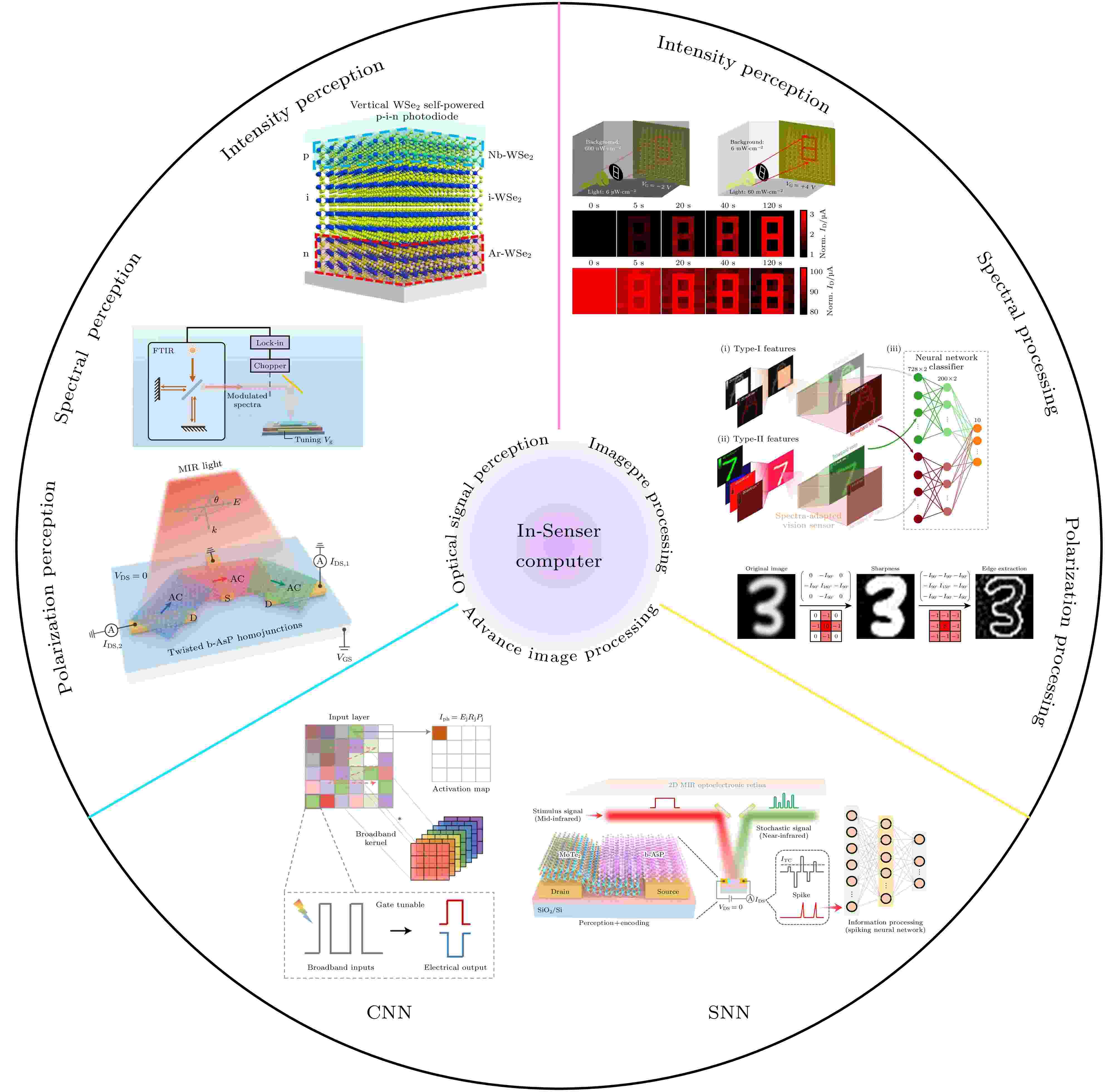
This paper provides a comprehensive review of recent advances in high-performance photodetectors based on two-dimensional materials and in-sensor computing for intelligent image processing, aiming to address the challenges of the “memory wall” and “power wall” caused by the separation of sensing, storage, and computing in traditional image sensors. Traditional image processing relies on the von Neumann architecture, where a large volume of raw data generated at the sensing end must be transmitted to independent computing units or cloud platforms for processing, leading to high energy consumption, significant latency, bandwidth burden, and security risks. Owing to their atomic thickness, high carrier mobility, weak short-channel effects, and tunable optoelectronic properties, two-dimensional (2D) materials provide an ideal physical foundation for achieving function integration of perception and computation. This paper discusses the topic from three perspectives: optical signal perception, image preprocessing, and advanced image processing. In terms of optical signal perception, 2D materials and their heterostructures exhibit ultrahigh responsivity, broadband operation, and fast response in light-intensity detection, enable miniaturized spectrometers through bandgap modulation and computational spectroscopy, and achieve compact, full-polarization analysis via twisted layers and metasurface structures. In image preprocessing, 2D material devices can perform convolution and feature extraction at the sensing end through linear photoresponse, suppress noise and extend dynamic range via superlinear and sublinear responses, and mimic biological visual adaptation in spectral and polarization domains to enhance image quality and robustness. In advanced image processing, the tunable photoresponse and memristive characteristics of 2D materials enable sensor-level integration of sensing, storage, and computation, This allows for the realization of matrix-vector multiplication and convolution operations within convolutional neural networks, significantly reducing power consumption and improving efficiency. Meanwhile, by implementing spike-rate and temporal encoding of optical signals in spiking neural networks, 2D material devices can achieve event-driven image recognition and classification under low-power and low-latency conditions. Furthermore, this paper highlights the challenges faced by 2D material image sensors, including scalable fabrication, heterogeneous integration with silicon technology, array- and circuit-level optimization, environmental stability and encapsulation, and system-level implementation, while envisioning their broad application prospects in intelligent imaging, wearable electronics, autonomous driving, and biomedical diagnostics. It is concluded that with the joint progress in materials science, device engineering, and artificial intelligence, 2D materials are expected to drive the development of next-generation low-power, high-performance, intelligent image processing platforms, and to become an essential foundation for future information perception and processing technologies.
EDITOR'S SUGGESTION
2025, 74 (22): 228502.
doi: 10.7498/aps.74.20251165
Abstract +
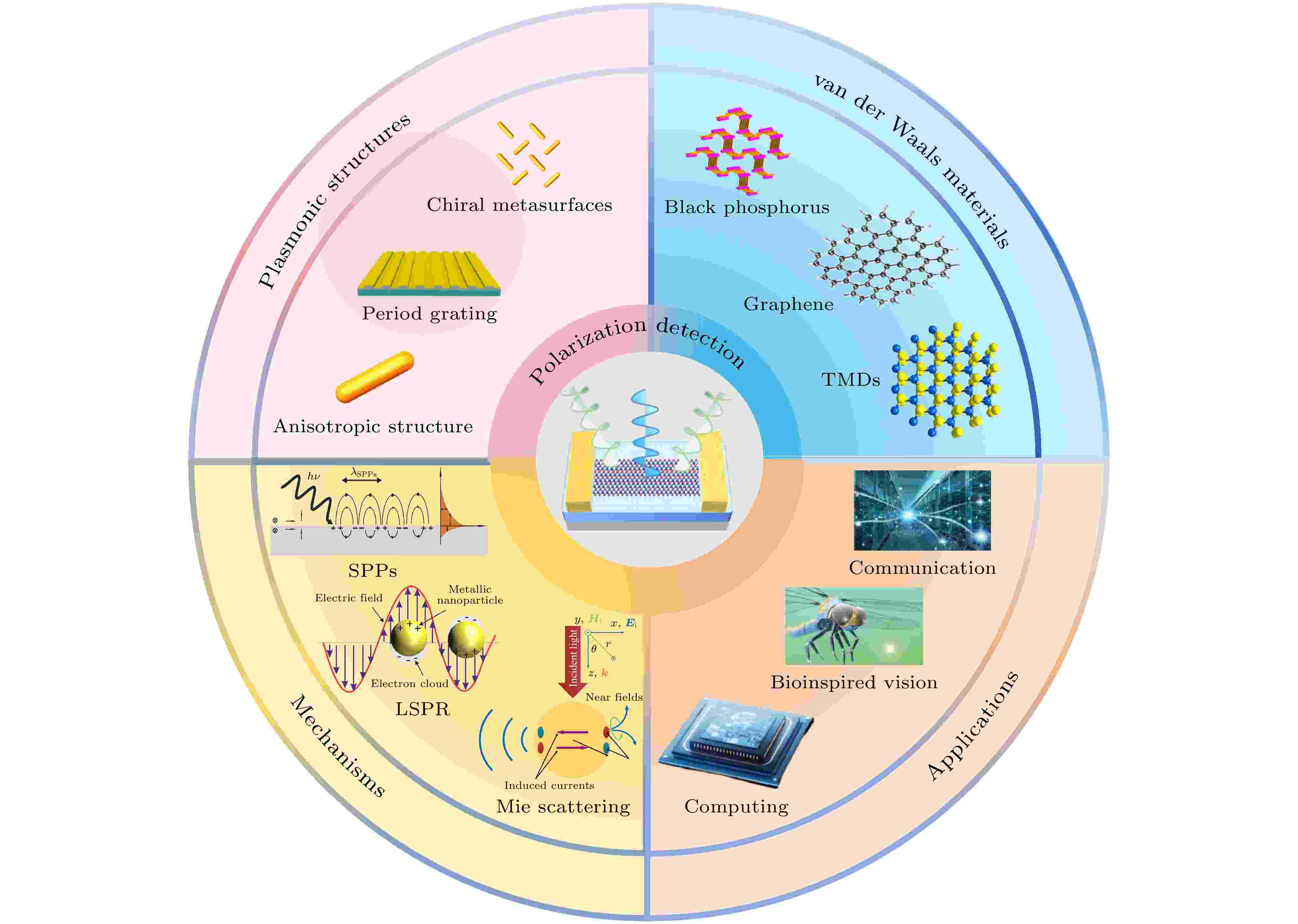
Polarization detection is a fundamental way to obtain the vectorial nature of light, supporting advanced technologies in the fields of optical communication, intelligent sensing, and biosensing. Two-dimensional van der Waals materials have become a promising platform for high-performance polarization-sensitive photodetectors due to their inherent anisotropy and tunable electronic properties. Nevertheless, their intrinsically weak light absorption and limited photoresponse efficiency remain major bottlenecks. Plasmonic nanostructures, which can achieve strong localized field confinement and manipulation on a nanoscale, provide an effective strategy to overcome these limitations and substantially improve device performance. In this review, we systematically summarize the coupling mechanisms between plasmonic architectures and vdW materials, highlighting near-field enhancement, plasmon-induced hot-carrier generation, and mode-selective polarization coupling as key physical processes for enhancing photocarrier generation and polarization extinction. Representative devices including metallic gratings, hybrid nanoantennas, and chiral metasurfaces are compared in terms of responsivity, detection speed, operating bandwidth, and polarization extinction ratio, revealing consistent improvements of one to two orders of magnitude over bare vdW devices. We further survey emerging applications in the fields of high-speed polarization-encoded optical communication, on-chip optical computing and information processing, and bioinspired vision and image recognition systems, where plasmonic-vdW hybrid detectors demonstrate unique advantages in miniaturization and energy efficiency. Finally, we discuss current challenges such as large-scale fabrication of uniform plasmonic arrays, spectral bandwidth broadening, and seamless integration with complementary photonic circuits, and outline future opportunities for next-generation polarization-resolved optoelectronic platforms.
EDITOR'S SUGGESTION
2025, 74 (22): 228503.
doi: 10.7498/aps.74.20251115
Abstract +
The increasing demands for high-speed imaging, aerospace, and optical communication have driven in-depth research on broadband photodetectors with high sensitivity and fast response. Two-dimensional (2D) materials have atomic-scale thickness, tunable bandgaps, and excellent carrier transport properties, making them ideal candidates for next-generation optoelectronics. However, their limited light absorption and intrinsic recombination losses remain key challenges. This paper provides an overview of recent progress of 2D-material-based broadband photodetectors. First, the fundamental optoelectronic properties of 2D materials, including bandgap modulation, carrier dynamics, and light–matter interactions, are discussed to clarify their broadband detection potential. Representative material systems, such as narrow-band gap semiconductors, 2D topological materials, and perovskites, are summarized, showing the detection ability from the ultraviolet to the mid-infrared regions. To overcome intrinsic limitations, four optimization strategies are highlighted: heterostructure engineering for efficient charge separation and extended spectral response; defect engineering to introduce mid-gap states and enhance sub-bandgap absorption; optical field enhancement through plasmonic nanostructures and optical cavities to improve responsivity; strain engineering for reversible band structure tuning, particularly suited for flexible devices. These strategies have achieved significant improvements in responsivity, detectivity, and bandwidth, with some devices implementing ultrabroadband detection and multifunctionality. In summary, 2D materials and their hybrids have shown great potential in broadband photodetection, with progress made in material innovation and device architecture optimization. The reviewed strategies, including heterostructure integration, defect modulation, optical field enhancement, and strain engineering, collectively demonstrate the different ways of overcoming intrinsic limitations and improving device performance. Looking ahead to the future, the reasonable combination of these methods is expected to further expand the detection window, improve sensitivity, and achieve multifunctional operations, thereby paving the way for the multifunctional applications of the next-generation broadband photodetectors in imaging, sensing, and optoelectronic systems.
EDITOR'S SUGGESTION
2025, 74 (22): 226301.
doi: 10.7498/aps.74.20251222
Abstract +
EDITOR'S SUGGESTION
2025, 74 (22): 227502.
doi: 10.7498/aps.74.20251066
Abstract +
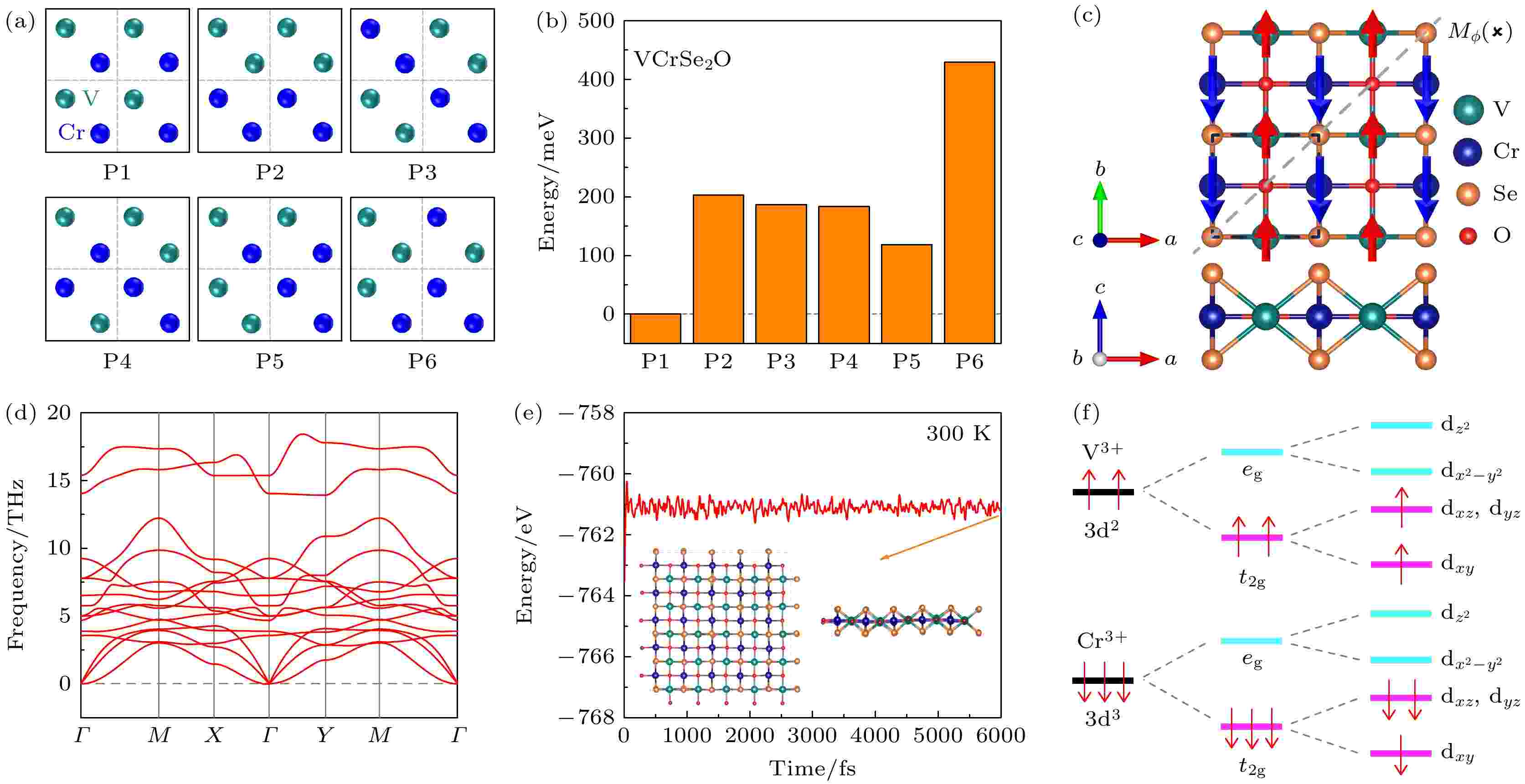
Stable and remarkable valley polarization effect is the key to utilizing valley degree of freedom in valleytronic devices. Recently, a novel collinear magnetic material known as altermagnet, which is different from ferromagnets and antiferromagnets, has attracted widespread attention. Theoretical studies have revealed that the monolayer altermagnet V2Se2O exhibits spin-valley locking induced by crystal symmetry rather than traditional time-reversal symmetry. Uniaxial strain can break the corresponding crystal symmetry, leading to a remarkable non-relativistic valley polarization effect. Therefore, beyond uniaxial strain, are there alternative strategies to break the crystal symmetry in altermagnets and achieve remarkable valley polarization? According to first-principles calculations and symmetry analysis, we reveal that valley polarization effect in monolayer V2Se2O altermagnet is correlated with the net magnetic moment between magnetic V atoms under uniaxial strain, thereby proposing two strategies for achieving giant valley polarization effect. Firstly, substituting one V atom in V2Se2O with Cr to construct a ferrimagnetic monolayer VCrSe2O enhances the net magnetic moment between magnetic atoms, thereby realizing a giant valley polarization effect. Applying uniaxial strain along either the a-axis or b-axis significantly increases the value of valley polarization, which exhibits a nearly linear relationship with the net magnetic moments between the magnetic atoms. Secondly, constructing a van der Waals heterostructure composed of V2Se2O and α-SnO monolayers breaks mirror symmetry, thereby inducing a net magnetic moment, which in turn causes a remarkable valley polarization effect. Compressing the interlayer distance of the heterostructure can increase the net magnetic moment between V atoms, thereby enhancing the value of valley polarization to nearly 400 meV. This work reveals that valley polarization in monolayer altermagnet is correlated with the net magnetic moment between magnetic atoms. Finally, we propose two strategies to achieve giant valley polarization based on monolayer altermagnets, providing theoretical guidance for the potential applications of ferrimagnetic monolayers and altermagnet-based heterostructures in valleytronics.
EDITOR'S SUGGESTION
2025, 74 (22): 228102.
doi: 10.7498/aps.74.20251070
Abstract +
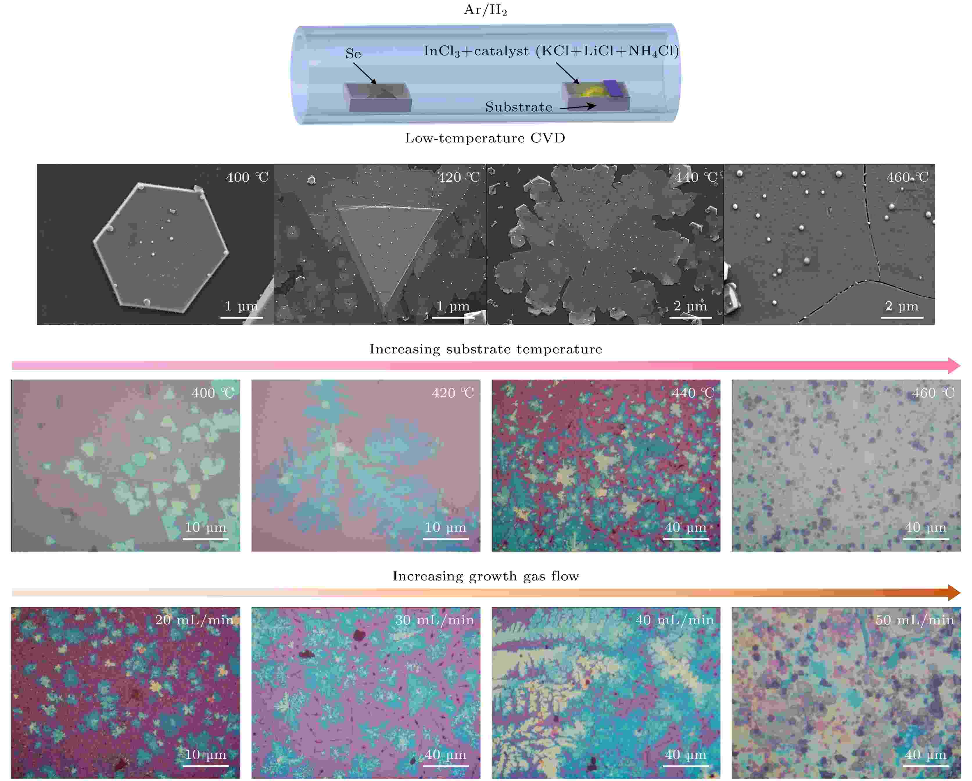
Two-dimensional ferroelectric α-In2Se3 possesses many fascinating physical properties. However, chemical-vapor-deposited ferroelectric α-In2Se3 typically requires high temperatures (>650 ℃). In this work, α-In2Se3 is synthesized at 400 to 460 ℃ by introducing a KCl/LiCl/NH4Cl ternary catalyst, resulting in a 200 ℃ reduction in growth temperature compared with ferroelectric α-In2Se3 synthesized by the traditional chemical vapor deposition (CVD) method. The surface morphology of the as-prepared material is controlled by temperature and gas flow rate. As the growth temperature increases from 400 to 460 ℃, the synthesized α-In2Se3 is changed from discrete hexagonal flakes to a continuous and uniform thin film, which is confirmed by the scanning electron microscope. Raman spectroscopy shows that the characteristic peaks of In2Se3 are located at 103, 180, and 195 cm–1, respectively, indicating that the CVD-grown In2Se3 is α-phase. Furthermore, energy dispersive spectrometer and X-ray photoelectron spectroscopy indicate that the elemental composition is close to the ideal stoichiometric ratio, confirming the successful synthesis of the α-In2Se3. Then, the as-prepared α-In2Se3 is transferred onto Si/SiO2 substrate for device fabrication. Atomic force microscope indicates that the film is uniform, with an approximate thickness of 63 nm. The fabricated two-terminal memristors exhibit analogous resistive switching behaviors. And such memristors are used to achieve synaptic functions of long-term potentiation/long-term depression. For artificial neural network simulations based on the synaptic memristors, the recognition accuracy for hand-written digit image exceeds 90%. This work provides a practical method for growing two-dimensional ferroelectric α-In2Se3 at low temperatures for applications in synaptic devices and neuromorphic computing.
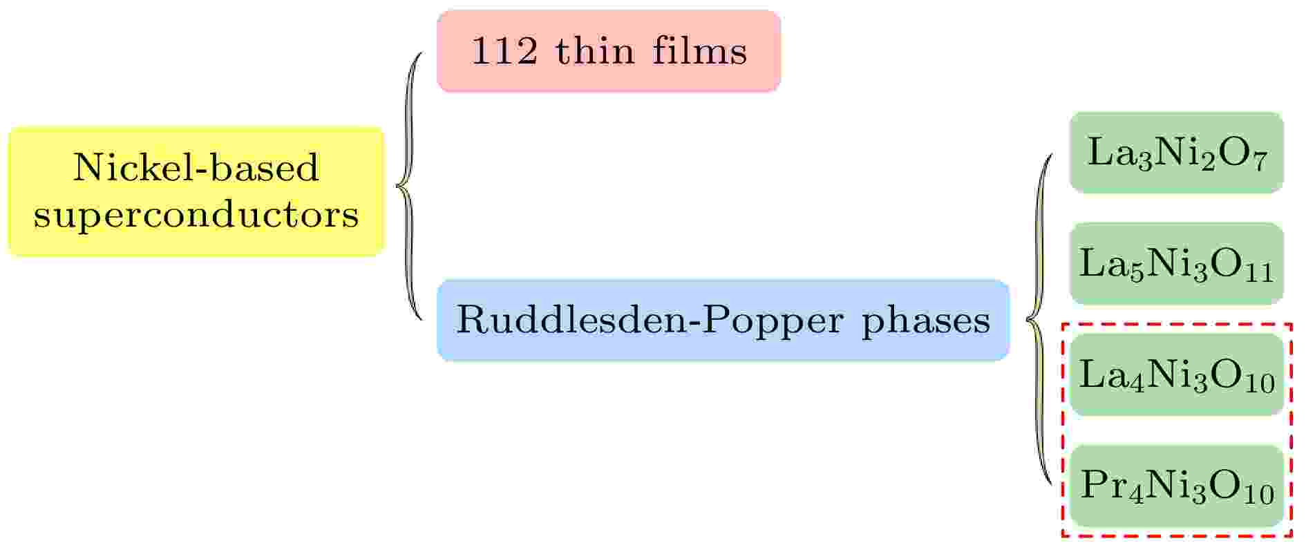
SPECIAL TOPIC—Research progress on nickelate superconductors
EDITOR'S SUGGESTION
2025, 74 (22): 227401.
doi: 10.7498/aps.74.20251179
Abstract +
EDITOR'S SUGGESTION
2025, 74 (22): 227402.
doi: 10.7498/aps.74.20251258
Abstract +
The recent discovery of high-temperature superconductivity in the bilayer nickelate La3Ni2O7 under high pressure has drawn significant attention, further catalyzing intensive research on nickel-based superconductors. Systematic comparative studies of unconventional superconductors are vital for advancing the mechanistic understanding of high-Tc superconductivity. In contrast to cuprates, bulk nickelates exhibit significant differences in crystal structure, electronic properties, and physical behaviors, and their experimental investigation faces specific challenges including the influences of hydrostatic conditions on the measurements of zero resistance and diamagnetic response, oxygen vacancy defects in single crystals, and pressure-induced structural phase transitions. This review comprehensively examines high-temperature superconductivity and the related research challenges in trilayer nickelate bulk materials, and provides experimental insights for future studies on nickel-based superconducting systems.
EDITOR'S SUGGESTION
2025, 74 (22): 227404.
doi: 10.7498/aps.74.20250903
Abstract +
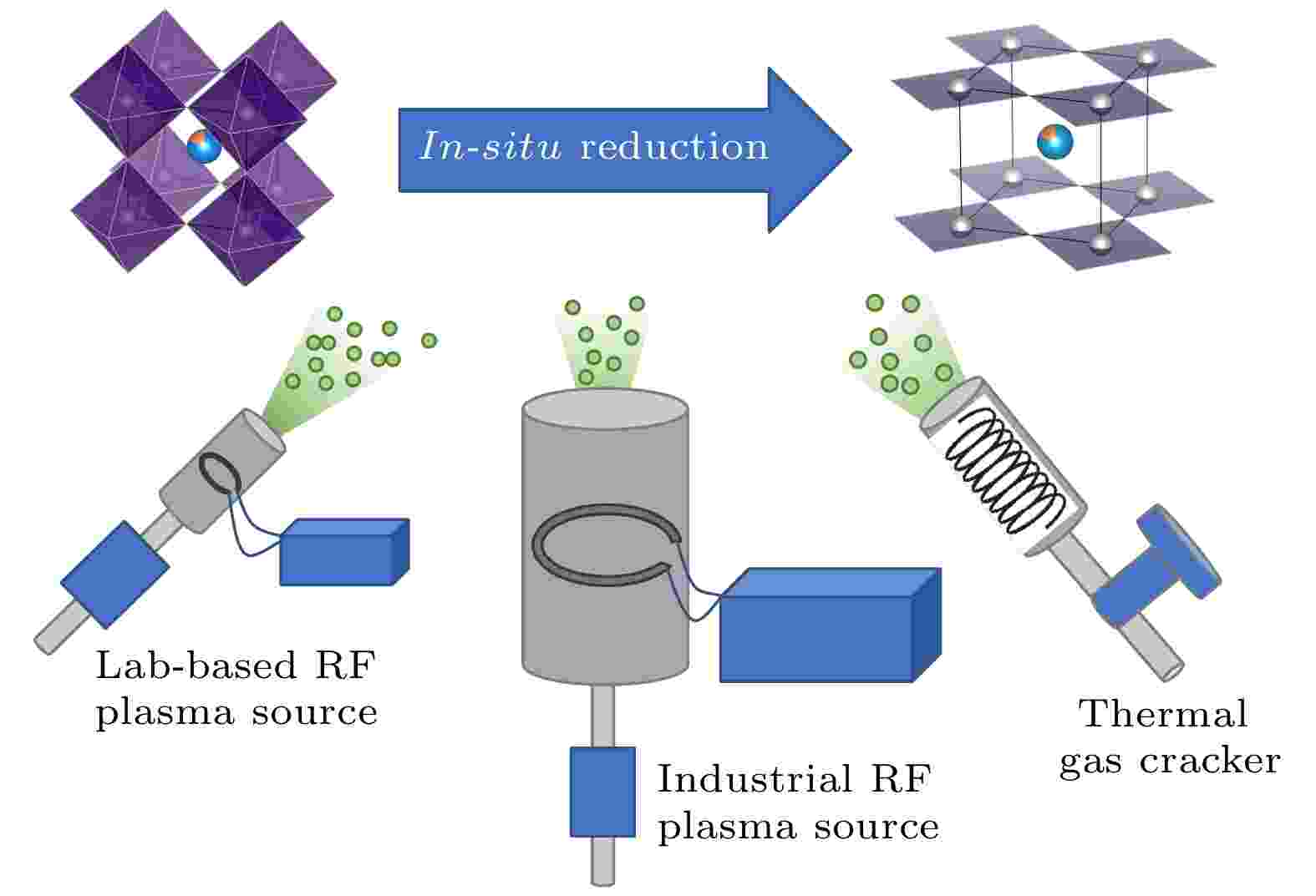
Infinite-layer nickelates, obtained by removing the apical oxygen from perovskite precursors, are the first nickelate system to exhibit superconductivity and provide a platform for exploring unconventional superconductivity. Although the traditional CaH2 sealed-tube reduction method is simple and effective, it is an ex-situ process that tends to cause surface contamination or degradation, making it unsuitable for surface-sensitive measurements like angle resolved photoemission spectroscopy (ARPES). To address this issue, we establish three different in-situ atomic hydrogen reduction methods in an ultrahigh vacuum chamber—namely, a lab-based RF plasma cracker, an industrial RF plasma cracker, and a thermal gas cracker. The key parameters including hydrogen flow, RF power or filament temperature, reduction temperature, and timeare comprehensively optimized using each of the above methods. Structural evolution is monitored by X-ray diffraction (XRD), surface morphology is characterized by atomic force microscopy (AFM), and superconducting properties are examined through electrical transport measurements. The results show that all three in-situ methods can achieve reduction and superconducting properties comparable to or better than CaH2 reduction. Moreover, all atomic hydrogen approaches yield lower surface roughness than CaH2 from the same precursor, highlighting their clear advantage in enhancing surface flatness. Notably, the industrial RF plasma source, due to its higher hydrogen production efficiency, enables sufficient reduction under milder conditions, resulting in even smoother surfaces. This study also provides a detailed summary of the parameter optimization for each method, providing valuable guidance for the controlled reduction of high-quality infinite-layer nickelate thin films.
SPECIAL TOPIC—Research progress on nickelate superconductors·COVER ARTICLE
COVER ARTICLE
2025, 74 (22): 227403.
doi: 10.7498/aps.74.20251080
Abstract +
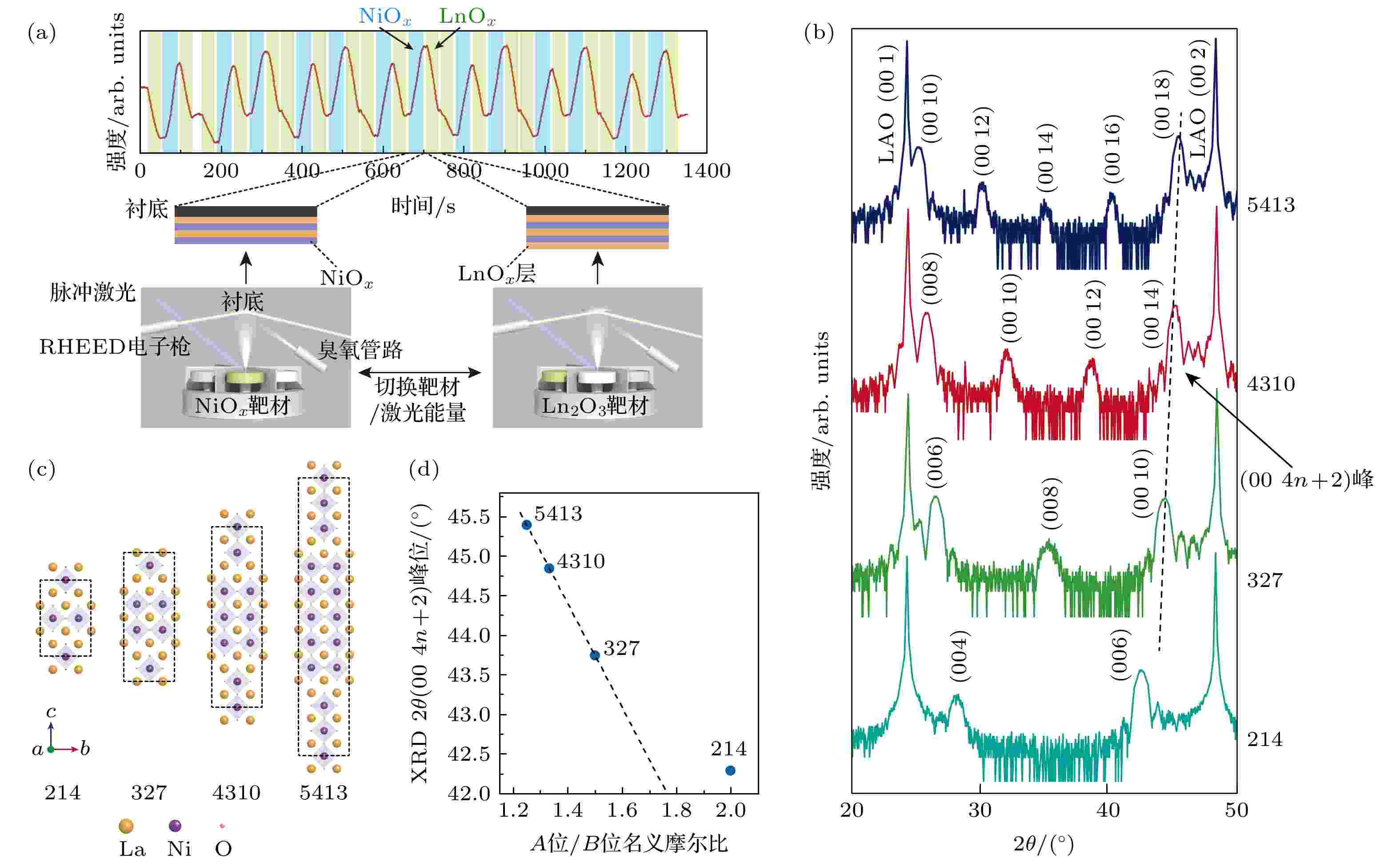
The discovery of ambient-pressure nickelate high-temperature superconductivity provides a new platform for further exploring the underlying superconducting mechanisms. However, the thermodynamic metastability of Ruddlesden-Popper nickelates Lnn+1NinO3n+1 (Ln = lanthanide) poses significant challenges for precise control over their structures and oxygen stoichiometry. This study establishes a systematic approach to growing phase-pure, high-quality Ln3Ni2O7 thin films on LaAlO3 and SrLaAlO4 substrates by using gigantic-oxidative atomic-layer-by-layer epitaxy. The films grown under an ultrastrong oxidizing ozone atmosphere are superconducting without further post-annealing. Specifically, the optimal Ln3Ni2O7/SrLaAlO4 superconducting film exhibits an onset transition temperature (Tc,onset) of 50 K. Four critical factors governing the crystalline quality and superconducting properties of Ln3Ni2O7 films are identified as follows. 1) Precise cation stoichiometric control suppresses secondary phase formation. In an Ni-rich sample (+7%), the thin film forms an Ln4Ni3O10 secondary phase, and the R-T curve correspondingly exhibits metallic behavior. In contrast, an Ni-deficient sample forms an Ln2NiO4 secondary phase, with its R-T curve indicating insulating behavior over the entire temperature range. 2) Complete atomic layer-by-layer coverage minimizes stacking faults. Deviation from ideal monolayer coverage induces in-plane atomic number mismatch, which directly triggers out-of-plane lattice collapse or uplift near bulk-equilibrium positions. 3) Optimized interface reconstruction can improve the atomic arrangement at the interface. This can be achieved through methods such as annealing the SrLaAlO4 substrate or pre-depositing a 0.5-unit-cell-thick Ln2NiO4-phase buffer layer, which enhances the energy difference between the Ln-site and Ni-site layers to promote proper stacking. 4) Accurate oxygen content regulation is essential for achieving a single superconducting transition and high Tc,onset. Although the under-oxidized sample demonstrates a relatively high Tc,onset (50 K), it displays a two-step superconducting transition. Conversely, the over-oxidized sample exhibits a reduced Tc,onset of 37 K and similarly manifests a two-step transition. These findings provide valuable insights into the layer-by-layer epitaxy growth of diverse oxide high-temperature superconducting films.
SPECIAL TOPIC—Thematic data in nuclear physics: Experimental, theoretical and applied research
EDITOR'S SUGGESTION
2025, 74 (22): 222801.
doi: 10.7498/aps.74.20250928
Abstract +
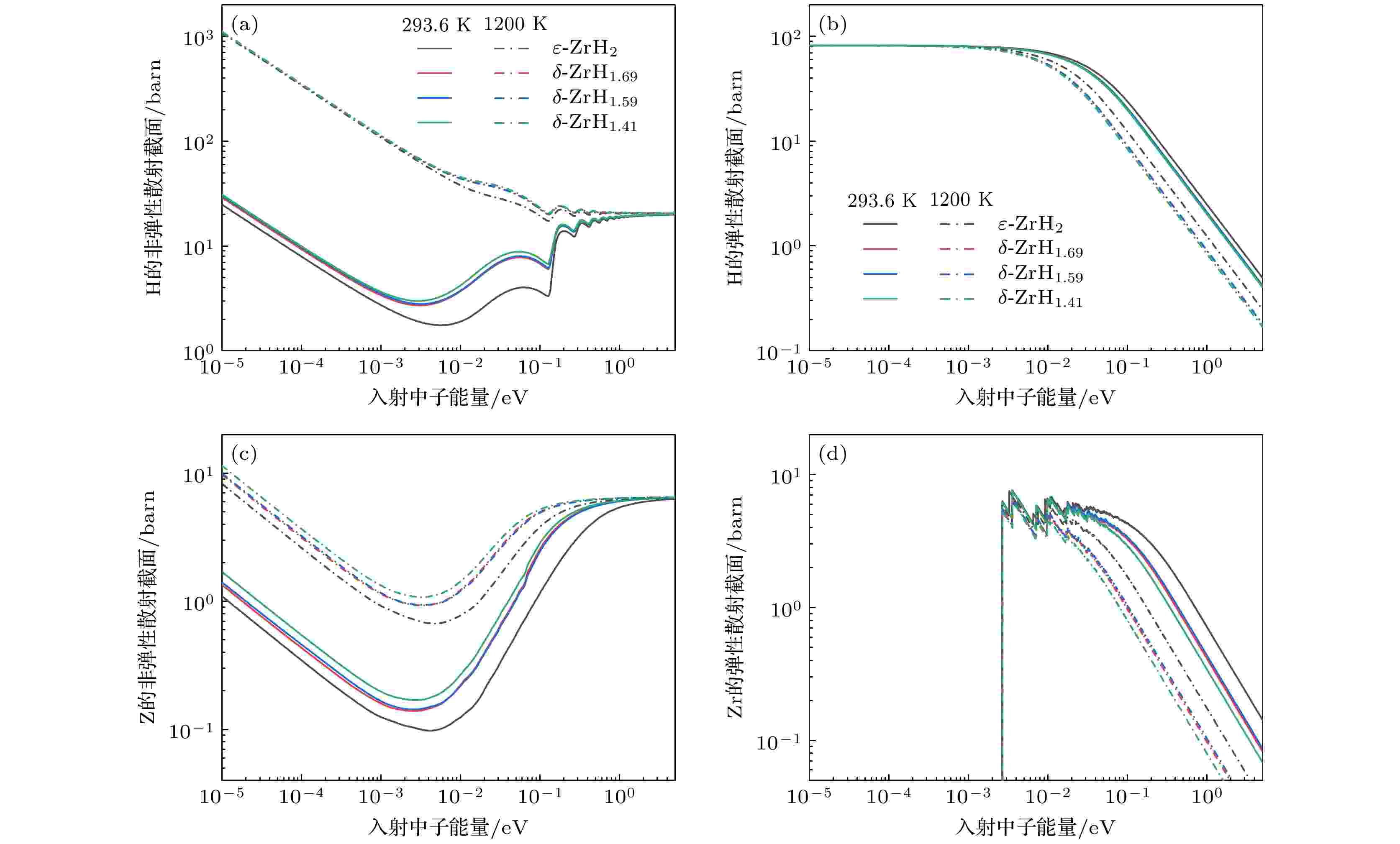
Metal hydrides are promising moderator materials in advanced reactors, where their thermal neutron scattering cross sections significantly affect the accuracy of reactor design. This study uses special quasi random structure (SQS) and first-principles lattice dynamics methods to calculate parameters such as the phonon densities of states of sub-stoichiometric zirconium hydride (ZrHx) and yttrium hydride (YHx). Based on these parameters, thermal scattering law (TSL) data for sub-stoichiometric hydrides are generated using the nuclear data processing code NECP-Atlas. The influences of hydrogen content on the thermal scattering cross sections of hydrides and the effective multiplication factor (keff) values of critical assemblies are analyzed. The result shows that variations in hydrogen content within hydrides lead to differences in thermal scattering cross sections, consequently affecting the neutron transport calculations of nuclear reactor. For the ICT003 and ICT013 benchmarks loaded with ZrHx (with H/Zr ≈ 1.6), using the TSL data derived from ZrHx with other hydrogen content results in a maximum deviation of 104 pcm in keff. For the HCM003 benchmarks loaded with ZrH2, the use of TSL from ZrHx with other hydrogen content leads to a maximum deviation of 147 pcm in keff.
GENERAL
2025, 74 (22): 220201.
doi: 10.7498/aps.74.20251026
Abstract +
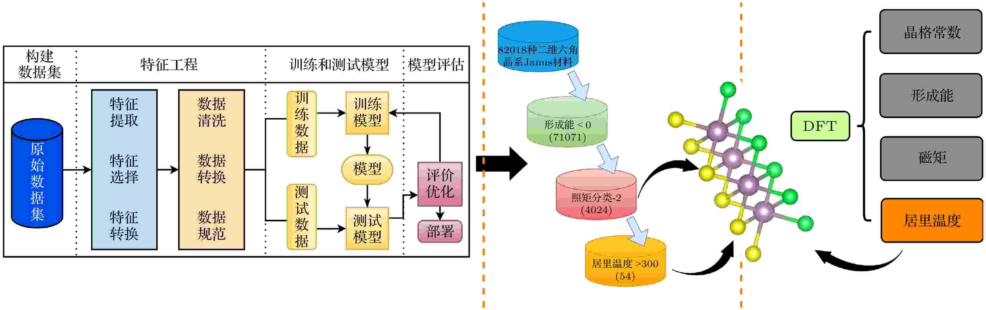
Magnetic skyrmions, characterized by their topological properties, serve as core components for developing next-generation non-volatile memory devices that demand high density, high speed, and low power consumption. Two-dimensional Janus magnetic materials inherently break spatial inversion symmetry, and easily generate strong DMI, providing an ideal platform for skyrmion generation and novel racetrack memory applications. Identifying high Curie temperature (Tc) materials is essential for ensuring magnetic stability and high-temperature application viability. This study integrates literature and open-source databases to construct a dataset of 16880 ABC-type two-dimensional materials. By utilizing stoichiometric ratios, intrinsic elemental properties, and electronic structure features as descriptors, four machine learning models, i.e. random forest (RF), gradient boosting decision tree (GBDT), extreme gradient boosting (XGBoost), and extra trees (ET) are employed for Tc prediction. Model performance is evaluated via ten-fold cross-validation, revealing that the XGBoost model exhibits superior prediction accuracy and generalization capability. Leveraging this model, Tc is predicted for 4024 unexplored two-dimensional Janus materials. This screening identifies 54 promising candidates possessing thermal stability, high magnetic moment, and a Tc exceeding 300 K. To verify reliability, four candidate systems (EuFeO, GdKTi, DyFeTb, ErFeGd) are randomly chosen for theoretical validation by using first-principles calculations combined with the Heisenberg model. For systems exhibiting strong correlation effects (containing d-orbital electrons), the Hubbard U parameter is included to describe on-site Coulomb repulsion. Exchange coupling constants are derived using the VASP software package. Subsequently, Tc values are calculated via classical Monte Carlo simulations performed using the MCSOLVER program. The research results show that the mean absolute error (MAE) of the predicted Tc is in good agreement with the model calculations for EuFeO and GdKTi, while larger deviations are observed for DyFeTb and ErFeGd. Nevertheless, the calculated Tc values for all four candidates exceed room temperature. This work establishes a new computational framework for the efficient screening of high-performance two-dimensional Janus magnetic materials, contributing to the advancement of magnetic storage technologies.
2025, 74 (22): 220701.
doi: 10.7498/aps.74.20250944
Abstract +
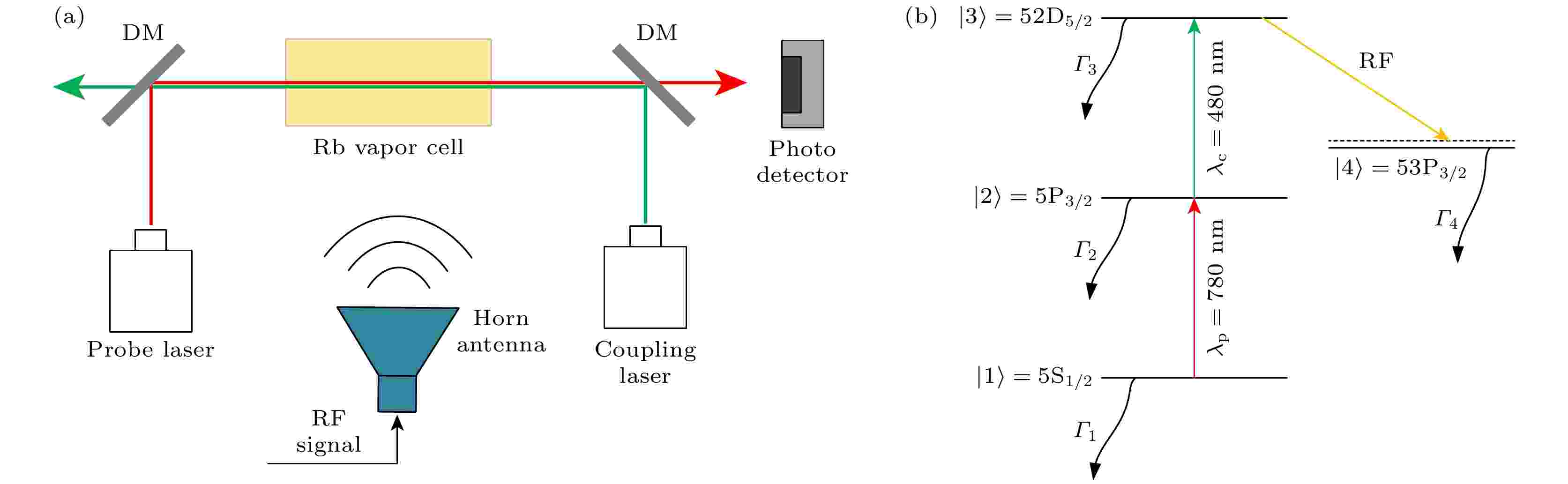
Rydberg atoms possess a large electric dipole moment and exhibit high sensitivity to electromagnetic signals. Receivers based on Rydberg atoms represent a novel reception mechanism, demonstrating broad application prospects in the field of communication. Current research has not addressed the influence of the operating parameters of Rydberg atomic receiver on channel capacity. This study establishes a channel capacity model for Rydberg atomic receiver based on Shannon's formula and the response mechanism of the electromagnetically induced transparency (EIT) effect. Using this model, the influences of atomic number density, laser beam waist, and coupling laser Rabi frequency on the channel capacity of Rydberg atomic receiver are analyzed. A strategy for optimizing channel capacity by adjusting the coupling laser Rabi frequency is proposed, and an analytical solution for the Rabi frequency that maximizes channel capacity is derived. The accuracy of this analytical solution is then verified through numerical simulations. The channel capacity corresponding to the analytical solution in this study is similar to the optimal channel capacity obtained using the one-dimensional optimization method (Newton’s method) and is superior to the results obtained by the quadratic interpolation method, demonstrating the effectiveness of the proposed analytical solution in optimizing the channel capacity of Rydberg atomic receiver. This research provides theoretical guidance for designing high-performance Rydberg atomic receiver and optimizing channel capacity.
CONDENSED MATTER: ELECTRONIC STRUCTURE, ELECTRICAL, MAGNETIC, AND OPTICAL PROPERTIES
EDITOR'S SUGGESTION
2025, 74 (22): 220702.
doi: 10.7498/aps.74.20250892
Abstract +
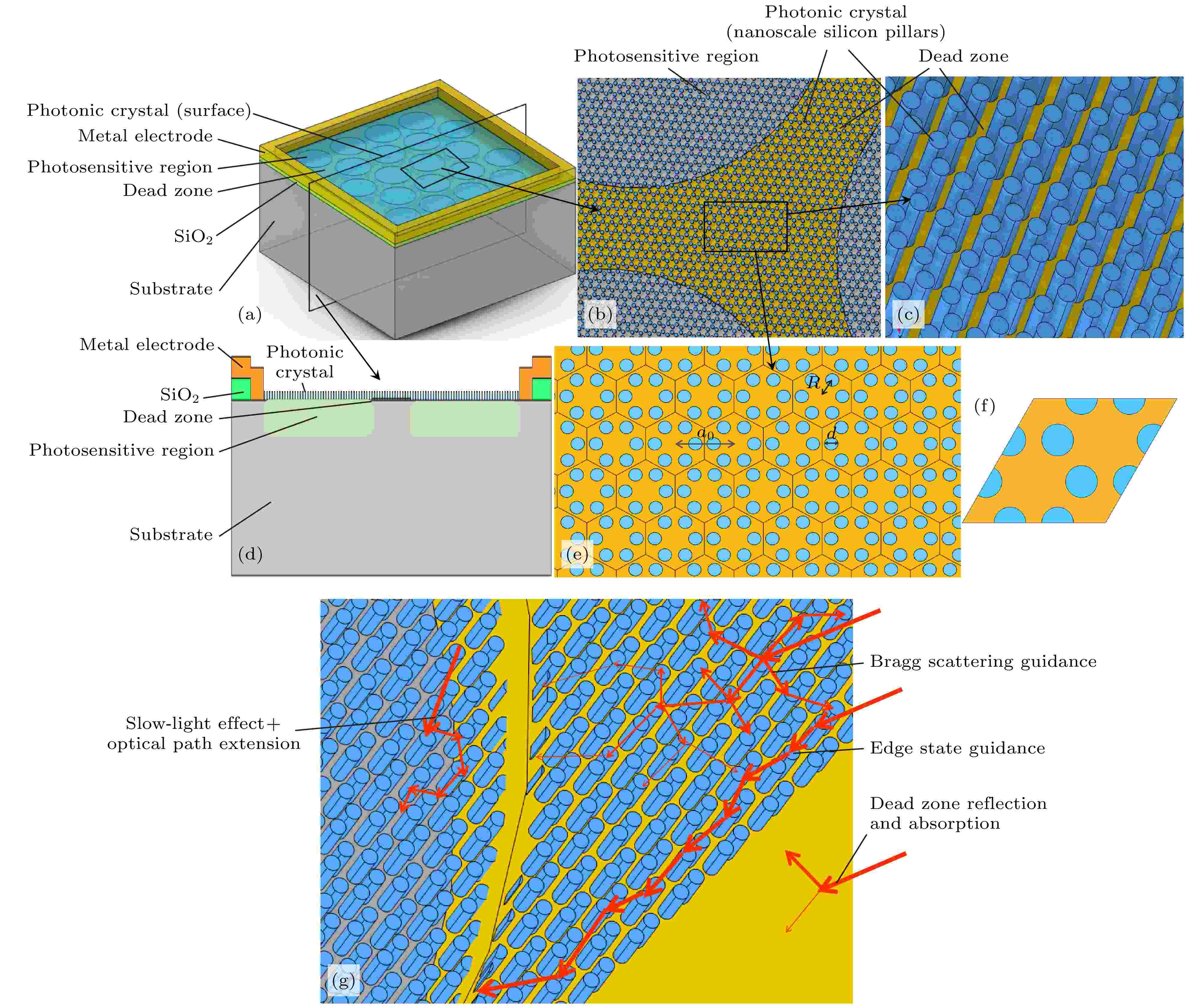
Silicon photomultipliers (SiPMs) have been widely used in the field of weak light detection. However, SiPMs utilizing small-sized Geiger-mode avalanche photodiode (G-APD) cells face the limitations due to a restricted effective geometric fill sactor (GFF), which leads to relatively low photon detection efficiency (PDE), and additionally, constrained by the intrinsic properties of silicon materials, their PDE in the near-infrared band is also relatively insufficient. To address the above issues, this work proposes a regional optical field modulation approach based on topological photonic crystals (TPCs), aiming to improve the PDE of SiPMs without modifying their internal structure. Through COMSOL electromagnetic wave frequency-domain simulation, the multi-band synergistic mechanism of dead-zone topological edge state guidance, photosensitive region slow-light effect, and Bragg scattering is revealed. In the 460–700 nm band, the honeycomb lattice in the dead zone induces topological edge states via Floquet periodic analysis, while the periodic dielectric distribution of the lattice excites Bragg scattering to reduce photon reflection loss at the metal surface and precisely couples photons to the photosensitive region, leading to an increase in effective GFF from 46.4% to 63.1% at 621 nm. In the 700–1100 nm band, in addition to reducing reflection loss via Bragg scattering, the designed periodic silicon pillar structure can effectively extend the transverse propagation path of photons through the slow-light effect, thereby increasing the coupling probability with the photosensitive region, resulting in a significant increase in absorption efficiency from 41.19% to 55.94% at 900 nm. Simulation results show that this design scheme increases the average PDE of SiPMs by 50% in the 460–1100 nm band (with a peak value of 81%) and can be implemented via mainstream etching processes (electron beam lithography + reactive ion etching). Compared with traditional microlens and plasmonic structures, TPCs exhibit significant advantages in broad-spectrum response and process simplification. This work provides a new topological photonics approach for photon recycling and PDE enhancement of SiPMs.
ATOMIC AND MOLECULAR PHYSICS
2025, 74 (22): 223101.
doi: 10.7498/aps.74.20251196
Abstract +
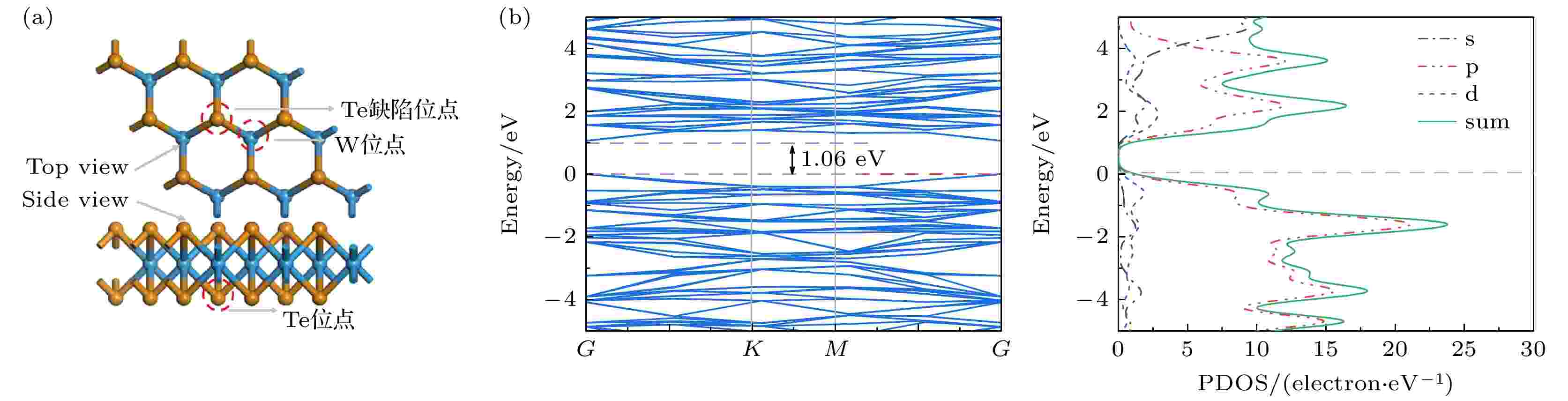
Using first-principles calculations based on density functional theory with a plane-wave ultrasoft pseudopotential approach, we conduct computations using the CASTEP (Cambridge Sequential Total Energy Package) module within the Materials Studio software. The electronic band structures, densities of states, and optical properties of intrinsic monolayer WTe2, monolayer WTe2 with a single tellurium vacancy (VTe), and rare-earth-doped VTe-containing monolayer WTe2 (VTe-X, where X = Ce, Yb, Eu) are systematically investigated to explore the synergistic effects of rare-earth doping and tellurium vacancy defects on the optical properties of monolayer WTe2. The results indicate that compared with the VTe model, the VTe-X models lead to a more pronounced enhancement of the optical performance in the infrared region (0–1.2 eV). All of VTe-X structures exhibit metallic characteristics, with a notable increase in the density of states near the Fermi level. In particular, the VTe-Yb model demonstrates significant improvement in the infrared range: the absorption coefficient, reflectivity, static dielectric constant, and peak value of the imaginary part of the dielectric function are enhanced by factors of 3.76, 1.83, 2.63, and 24.20, respectively, compared with those of pristine monolayer WTe2. This study provides a theoretical foundation for designing infrared photodetectors based on monolayer WTe2 substrates.
EDITOR'S SUGGESTION
2025, 74 (22): 223201.
doi: 10.7498/aps.74.20251237
Abstract +
ELECTROMAGNETISM, OPTICS, ACOUSTICS, HEAT TRANSFER, CLASSICAL MECHANICS, AND FLUID DYNAMICS
2025, 74 (22): 224201.
doi: 10.7498/aps.74.20250828
Abstract +
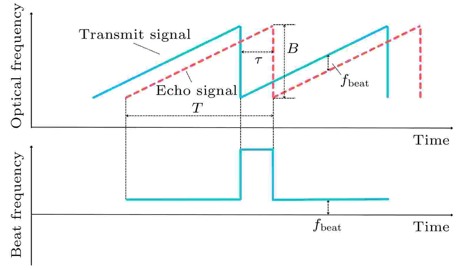
To address the frequency sweeping nonlinearity of frequency-modulated continuous-wave signals generated by a current-modulated distributed feedback laser diode, we propose and experimentally demonstrate a pre-distortion method based on a feedforward neural network. For this method, the beat frequency signals of the distributed feedback laser diode under a sawtooth-waveform current modulation are first experimentally obtained, and then the time-frequency curves of the distributed feedback laser diode output are obtained by performing a Hilbert transform on the beat signals. Subsequently, three-layer feedforward neural networks with 10, 5, and 3 hidden-layer neurons are constructed, respectively. By taking the driving current and the time-frequency curves as the input and output of the feedforward neural network, respectively, the nonlinear mapping relationship between them is established. Finally, a backpropagation algorithm is utilized to obtain the pre-distortion modulation current. Taking this current under the modulation frequency from 1 kHz to 10 kHz to drive the distributed feedback semiconductor laser (DFB-LD), the performance of the generated frequency-modulated continuous-wave (FMCW) signals is analyzed. We use nonlinear regression coefficients and residual root mean square values to characterize the performance. For the modulation frequency set at 4 kHz, the frequency sweeping nonlinearity and the residual root mean square value are reduced from 5.29×10⁻³ and 281 MHz to 1.77×10⁻⁵ and 15.15 MHz, respectively. With the modulation frequency fixed at 6 kHz, the frequency sweeping nonlinearity decreases from 5.58×10⁻³ to 1.52×10⁻⁵ and the residual root mean square declines from 251.98 MHz to 12.17 MHz in the proposed scheme. Across the entire tested frequency range from 1 kHz to 10 kHz, the nonlinearity remains stable at ~10–5 after adopting the pre-distortion scheme, with RMS values consistently below 20 MHz. The proposed method is expected to provide a new scheme for the linearization technology of the sweep signal in high-precision frequency-modulated continuous-wave light detection and ranging systems.
2025, 74 (22): 224202.
doi: 10.7498/aps.74.20251109
Abstract +
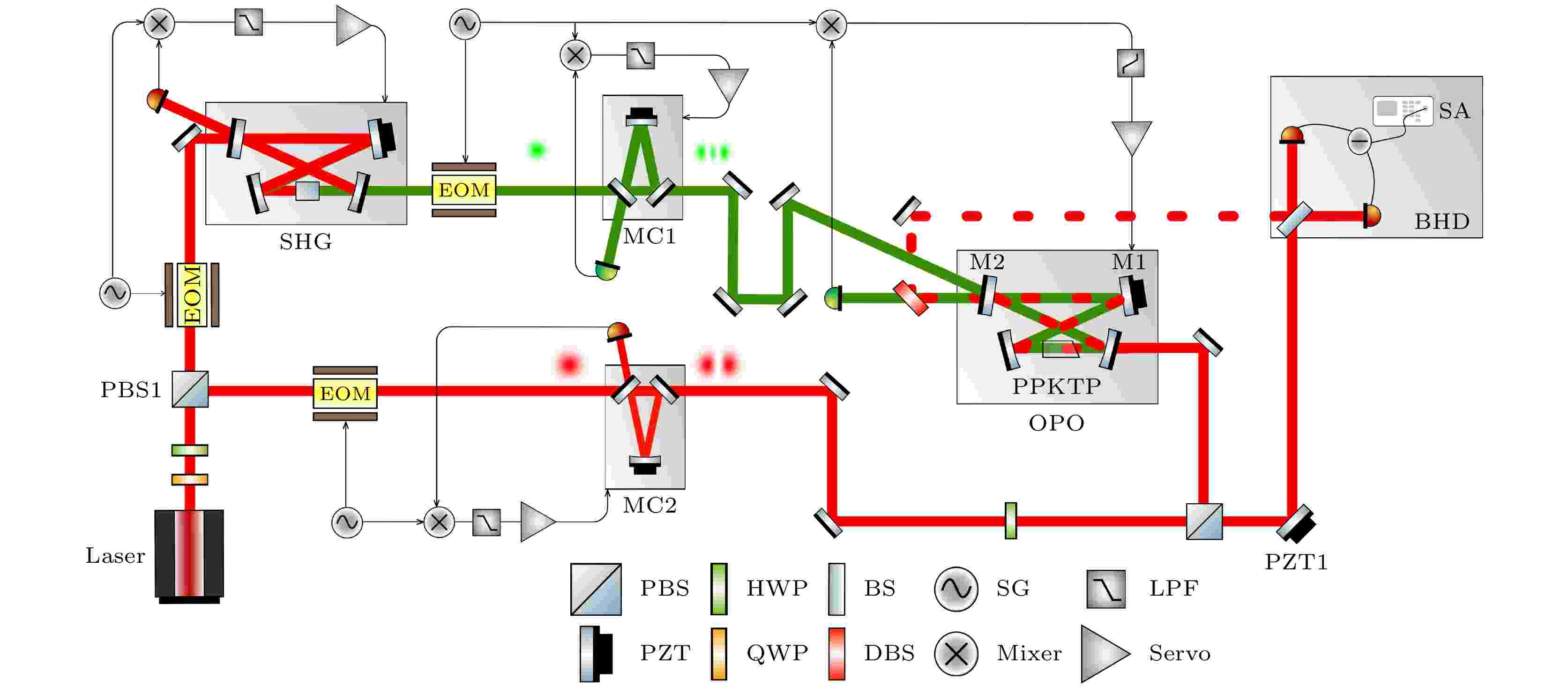
The high-order Hermite-Gaussian (HG) mode squeezed light, as one of the important quantum sources, has significant application in quantum precision measurement and quantum imaging. The enhancement of spatial measurement precision largely depends on the squeezing level of high-order HG-mode quantum states. However, the squeezing level of high-order HG modes is primarily limited by the external pump power in the optical parametric oscillator (OPO) cavity. As is well known, the OPO with dual resonance for both squeezed light and pump light can lower external pump power. The generation of HG10 mode squeezed light differs from that of HG00 mode squeezed light, with an additional Gouy phase shift introduced between the HG20 pump mode and HG10 down-conversion mode within the OPO cavity. In this work, we conduct theoretical analysis and experimental generation of HG10 mode squeezed light at lower external pump power by using a doubly-resonant OPO based on a wedged periodically poled KTiOPO4 (PPKTP) crystal. By precisely controlling both the propagation length of the optical field and temperature in the wedged PPKTP crystal, we simultaneously compensate for the Gouy phase shift between the HG20 and HG10 modes and the astigmatism induced by the frequency-dependent refractive index. This configuration allows for dual resonance of the HG20 pump mode and the HG10 squeezed mode, while operating under the condition close to optimal phase matching. Increasing the reflectivity of the input coupler of OPO cavity enhances the intra-cavity circulating power of the pump light, thereby reducing the required external pump power. Here, the bow-tie-shaped OPO cavity consists of two plane mirrors and two concave mirrors with a curvature radius of 50 mm. The wedged PPKTP is placed in the smallest beam waist of the cavity. The mode converter is employed to generate high-purity HG20 pump mode with a measured purity of 98.0%. The mode-matching effciency of 93.0% is achieved between the high-purity HG20 pump mode and the OPO cavity. The homodyne visibility of the HG10 mode is 98.1%. We experimentally demonstrate the generation of 9.10 dB HG10 mode squeezed light by using a doubly-resonant OPO with only 51 mW of HG20 pump mode, and simultaneously achieve 9.20 dB of squeezing in the HG00 mode with 27 mW of HG00 pump mode. The inferred squeezing levels of both HG10 mode and HG00 mode squeezed light both reach up to 12.15 dB. The quantum technology has solved the pump power limitations in optical parametric oscillators, generating high-order HG mode states with high squeezing level and providing an effective method for enhancing spatial measurement precision.
2025, 74 (22): 224701.
doi: 10.7498/aps.74.20250902
Abstract +
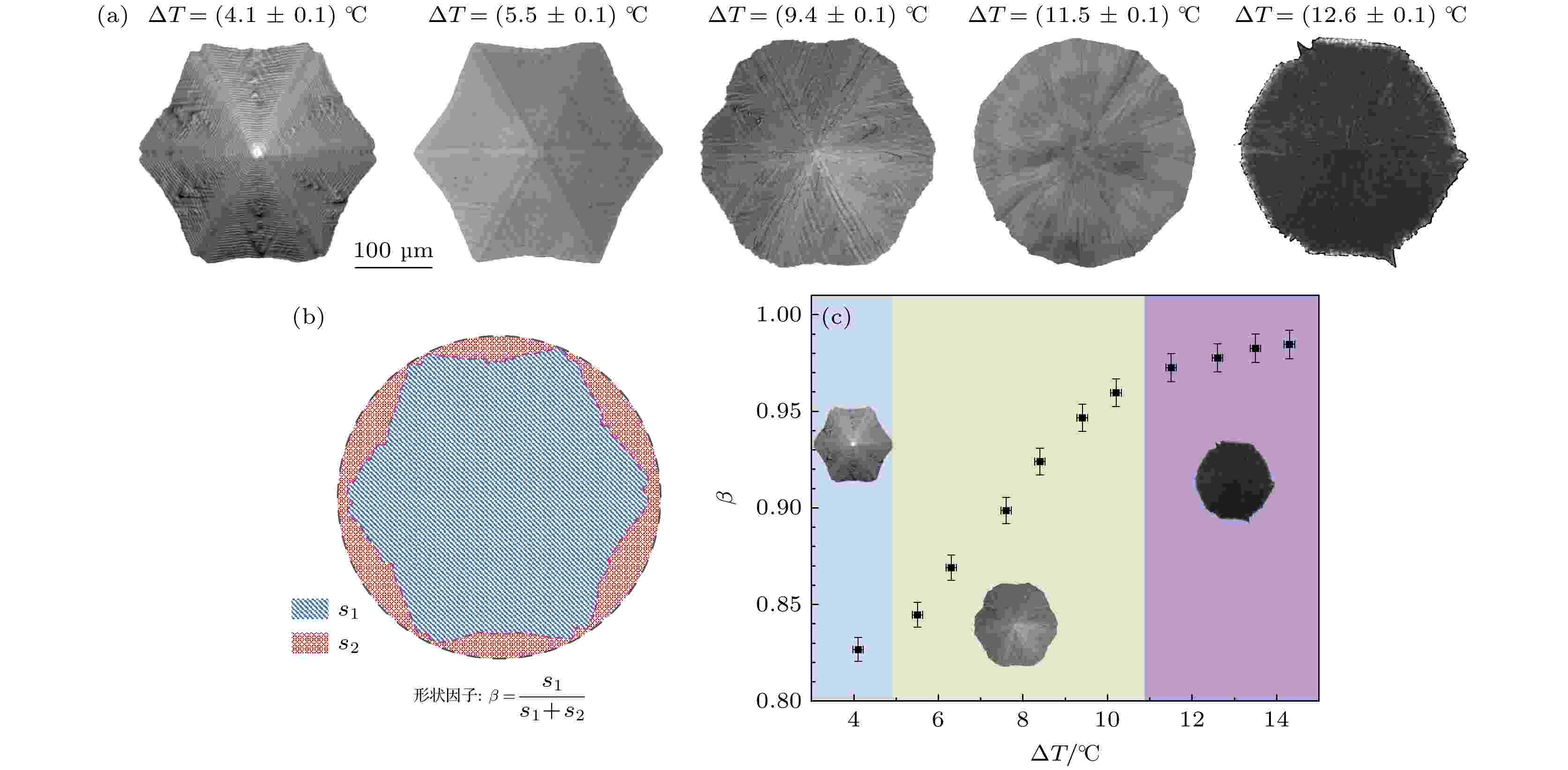
Freezing of multicomponent droplets and thin films is ubiquitous in natural environments and engineered settings. Previous studies on multicomponent droplets, including Marangoni-driven self-lifting droplets and soap-bubble freezing, have identified the roles of interfacial flow and solute redistribution, often exhibiting a snow-globe effect of migrating ice particles. Curvature and field-of-view constraints in droplet systems hinder continuous observation of a single object. Here, utilizing the comparability of interfacial heat and mass transfer between droplets and films, we employ a flat isopropanol-water binary film on a cooled substrate to achieve high-resolution, time-resolved in-situ microscopy observation of individual separated ice flakes within a supercooling (ΔT) range of the substrate. Experiments show that with the increase of ΔT, the external shape of ice flakes evolves from hexagonal pyramid to dodecagonal pyramid and ultimately to a nearly-conical form, accompanied by the decrease of transparency. We quantify morphological evolution by using a shape factor β and qualitatively distinguish crystal-structure differences by combining bright-field and dark-field microscopy. A minimal model that couples solute and thermal diffusion with Marangoni stress rationalizes the observations: solute-concentration gradients primarily drive structural evolution, while the competition between advection and diffusion governs anisotropic growth. These results provide mechanistic insight into interfacial freezing dynamics of multi-component liquid films and establish flat-film microscopy as a platform for single-flake kinetics.
PHYSICS OF GASES, PLASMAS, AND ELECTRIC DISCHARGES
2025, 74 (22): 225201.
doi: 10.7498/aps.74.20250952
Abstract +
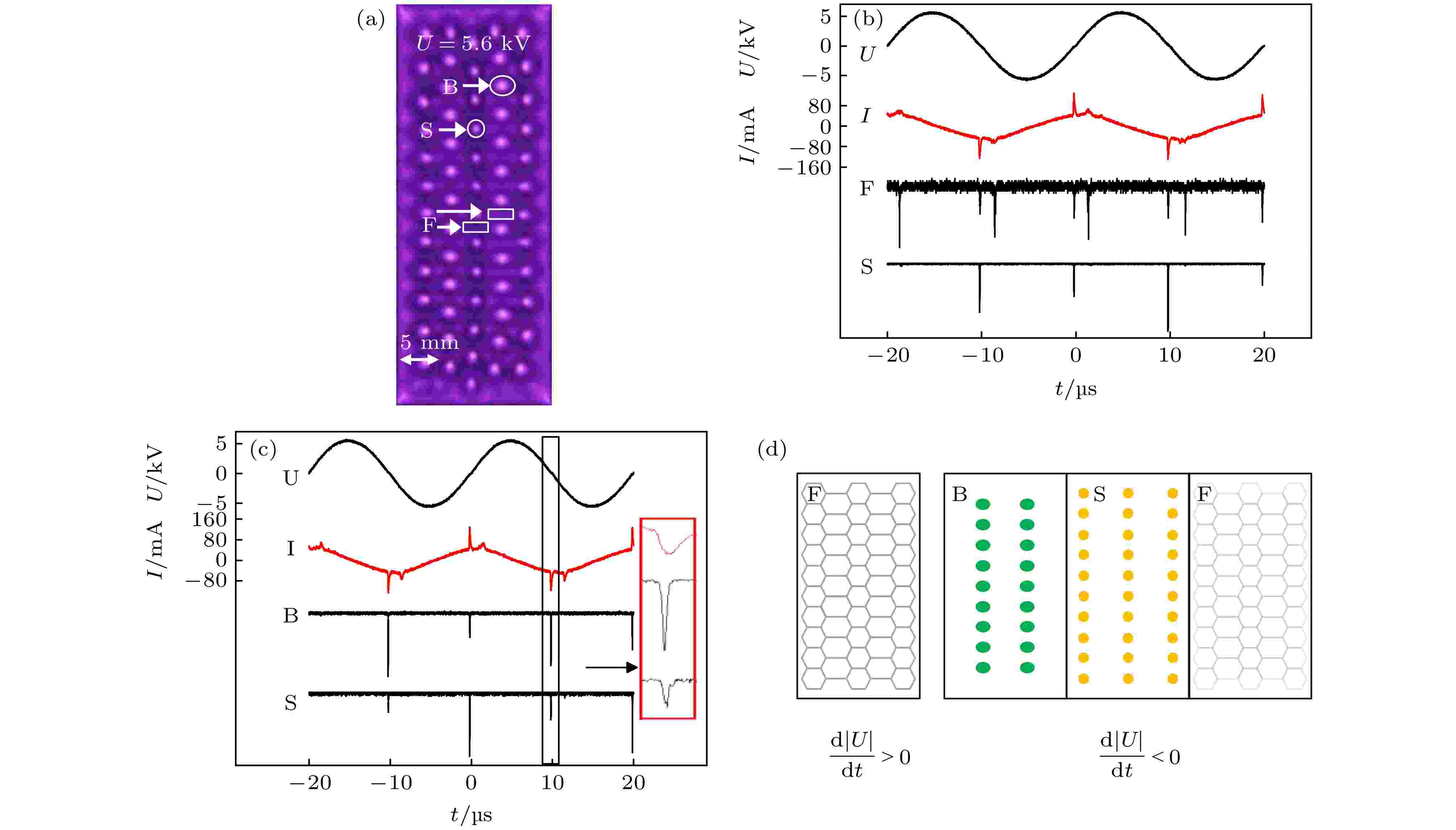
Patterns formed in dielectric barrier discharge is a typical nonlinear self-organization phenomenon. Research on the patterns helps elucidate the formation and evolution mechanisms of spatiotemporal structures in non-equilibrium systems, while also holding potential application value in fields such as material processing and plasma chemical engineering. A honeycomb superlattice pattern with an alternately-stretched honeycomb frame is observed in dielectric barrier discharge with a rectangular modulated gas gap for the first time and is studied both experimentally and theoretically. As the applied voltage increases, the pattern evolves from a hexagonal superlattice pattern with D6h symmetry to a quasi honeycomb superlattice pattern with D2h symmetry. Experimentally, the spatiotemporal structures of these two patterns are measured using an intensified charge coupled device (ICCD) and two photomultiplier tubes (PMTs). It is found that the hexagonal sublattice in the honeycomb superlattice pattern is divided into two sublattices, including a large stripe sublattice and a small stripe lattice. Additionally, the honeycomb frame sublattice is alternately-stretched. Discharges occur during both the rising and falling edges of the applied voltage. Through the estimation of the wall charge quantities of the two types of honeycomb frames and the analysis of the influence of boundaries on pattern formation, it is found that the quasi honeycomb superlattice pattern emerges as a self-organized structure under the influence of gas gap symmetry. Theoretically, the Poisson equation is numerically solved using COMSOL Multiphysics to simulate the electric field of the alternately-stretched honeycomb frame before and after discharge during the rising phase of the applied voltage. The result well explains the experimental phenomenon and provides the formation mechanism of the alternately-stretched honeycomb frame.
2025, 74 (22): 225202.
doi: 10.7498/aps.74.20250985
Abstract +
In this work, a special striped water electrode dielectric barrier discharge device is designed. Through numerical solutions of the Laplace equation, the spatial distribution of the applied electric field is revealed to exhibit a strip-shaped nonuniform distribution featuring the alternating regions of enhanced and weakened field intensity. These field gradients play a pivotal role in governing the plasma, for the intensified regions act as preferential sites for discharge onset, directly shaping the formation and evolution of plasma structures. Using this device, a series of novel striped patterns is observed in the discharge of a mixed gas of air and argon, marking a significant advancement in pattern formation studies. Notably, four striped superlattice patterns are obtained for the first time, each displaying intricate structural hierarchies. Among them, the large and small dot honeycomb striped superlattice pattern featuring structural complexity is chosen to investigate the formation mechanisms. The pattern is composed of three substructures: small dots, large dots, and a honeycomb framework. In the experiment, the emission spectra of different substructures are measured using a spectrograph, revealing that they are in different plasma states. The spatiotemporal dynamic behaviors of the pattern are observed using a high-speed camera and two photomultiplier tubes. It is found that the discharge sequence is small dots → large dots → honeycomb framework, where the honeycomb framework is formed by the superposition of random discharge filaments. The electric field distributions at different times are simulated by solving the Poisson equation, and the result well explains the formation mechanism of the above-mentioned patterns.
2025, 74 (22): 225203.
doi: 10.7498/aps.74.20251009
Abstract +
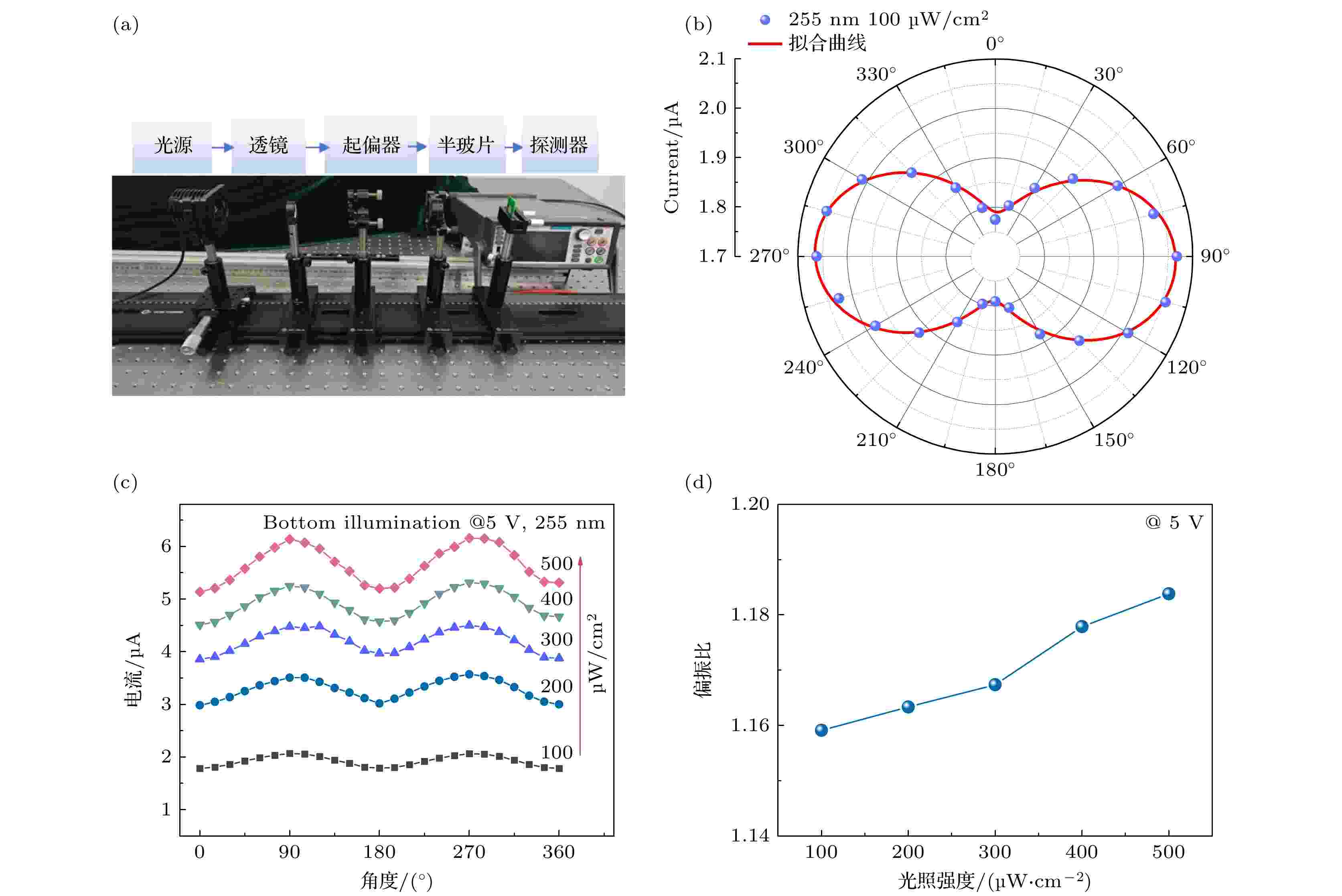
To meet the urgent demand for high-performance photodetectors in emerging solar-blind ultraviolet communication applications, this study systematically designs and implements a fully transparent β-Ga2O3 solar-blind photodetector based on a back-illumination architecture. The device is fabricated using RF magnetron sputtering to epitaxially grow high-quality β-Ga2O3 films (~300 nm in thickness, ~4.98±0.05 eV in bandgap) on double-polished sapphire substrates, with indium tin oxide (ITO) interdigitated electrodes forming efficient quasi-Ohmic contacts with n-type Ga2O3. The core advantage of this design lies in exploiting the high deep-UV transmittance of double-polished sapphire substrates, enabling incident photons to completely bypass the UV-absorbing ITO electrodes and eliminate photon loss caused by electrode shadowing effects in traditional front-illumination configurations. Consequently, the device demonstrates exceptional optoelectronic performance: a maximum responsivity of 0.46 A/W corresponding to an external quantum efficiency of 222.4%, an outstanding UV/visible rejection ratio of 1.2×10⁴, a minimum noise equivalent power of 1.52 pW/Hz1/2, and a peak specific detectivity of 1.39×10¹¹ Jones, with fast response times of 24 μs (rise) and 1.24 ms (decay). Building on this high-performance detector platform, we further explore its multifunctional application potential by constructing a polarization detection system that utilizes the intrinsic lattice anisotropy of monoclinic β-Ga2O3, and successfully demonstrating a non-line-of-sight (NLOS) UV communication system that validates high-fidelity information transmission in complex scattering channels. This work provides effective physical insights and experimental basis for developing next-generation Ga2O3-based optoelectronic devices with integrated high sensitivity, polarization resolution, and NLOS communication capabilities, showing promising applications in secure communications and polarization imaging.
CONDENSED MATTER: STRUCTURAL, MECHANICAL, AND THERMAL PROPERTIES
EDITOR'S SUGGESTION
2025, 74 (22): 226801.
doi: 10.7498/aps.74.20250873
Abstract +
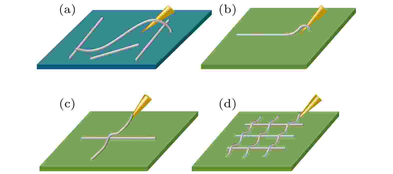
Adhesion at the nanowire-substrate interface plays a critical role in determining the performance, integration density, and long-term reliability of micro/nano devices. However, existing measurement techniques, such as peeling tests based on atomic force microscopy and in-situ electron microscopy techniques, often suffer from operational complexity, limited environmental applicability, and large measurement uncertainties. To solve these problems, this study proposes a cross-stacked bridge testing method based on optical microscopy nanomanipulation (OMNM), which can directly and quantitatively measure nanowire-substrate interfacial adhesion energy under ambient conditions. In this method, nanowires are precisely stacked on the target substrate to form a grid structure, where miniature bridges spontaneously appear at the intersections. The bridge geometry is governed by the mechanical balance between nanowire bending deformation and interfacial adhesion. By combining Euler–Bernoulli beam theory with the principle of energy conservation, a quantitative model is established to correlate arch geometry with adhesion energy, thereby realizing reliable measurement. Using this method, we measure the adhesion energies of SiC, ZnO, and ZnS nanowires on Si substrates. The SiC/Si system yields an adhesion energy of (0.154 ± 0.030) J/m2, which is in excellent agreement with the van der Waals (vdW) theoretical value (~0.148 J/m2), confirming that its interfacial behavior is dominated by vdW forces. In contrast, the measured adhesion energies for ZnO/Si ((0.120 ± 0.034) J/m2) and ZnS/Si ((0.192 ± 0.043) J/m2) are significantly higher than their corresponding vdW predictions (0.090 J/m2 and 0.122 J/m2, respectively). This discrepancy is attributed to surface polarization in ZnO and ZnS nanowires, which induces additional electrostatic attraction and thus enhances interfacial adhesion. These findings not only reveal the coupling mechanism between vdW forces and electrostatic interactions in polar nanowire systems but also provide new experimental evidence for understanding complex interfacial phenomena. The proposed OMNM-based cross-stacked bridge testing method offers advantages of operational simplicity, high accuracy, and broad applicability. In addition to nanowires, it can be extended to other low-dimensional nanostructures, such as nanotubes and two-dimensional materials. Looking forward, this approach holds promise as an efficient platform for building adhesion energy databases of realistic systems and for advancing mechanistic insights into interfacial adhesion. Furthermore, it can provide valuable guidance for the design, optimization, and reliability evaluation of next-generation nanoelectronic and optoelectronic devices, thereby contributing to micro/nano fabrication and functional device engineering.
INTERDISCIPLINARY PHYSICS AND RELATED AREAS OF SCIENCE AND TECHNOLOGY
2025, 74 (22): 228901.
doi: 10.7498/aps.74.20250803
Abstract +
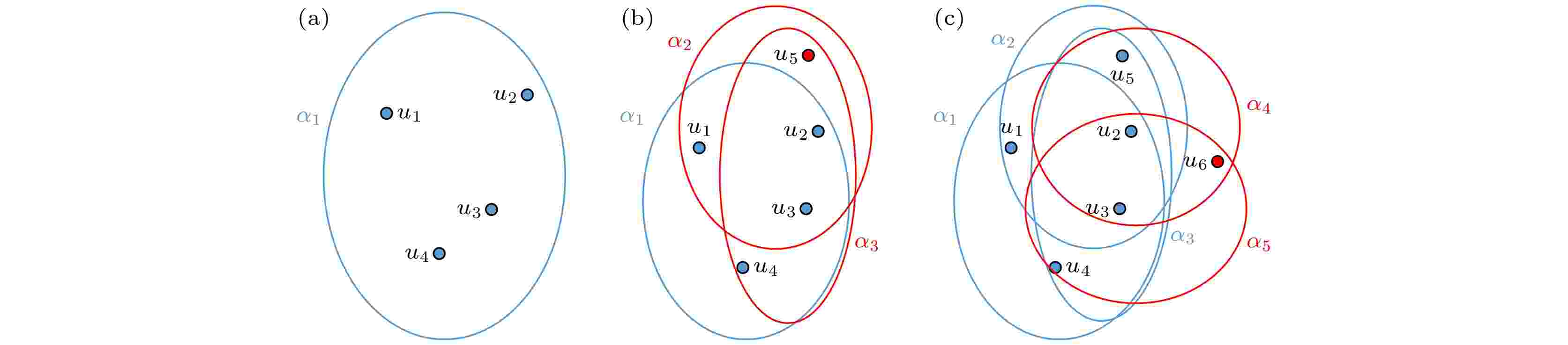
Complex networks are powerful tools for characterizing and analyzing complex systems, with wide applications in fields such as physics, sociology, technology, biology, shipping and port terminal management. One of the core issues in complex networks is the mechanism behind the emergence of scaling laws. In real-world networks, the mechanisms underlying the emergence of scaling laws may be highly complex, making it difficult to design network evolution mechanisms that fully align with reality. Explaining real networks through simple mechanisms is a meaningful research topic. Since Barabási and Albert discovered that growth and linear preferential attachment are mechanisms that generate power-law distributions, scholars have identified various forms of preferential attachment that produce power-law degree distributions. However, the most famous and useful one remains the linear preferential attachment in the BA model. Although complex networks have flourished over the past two decades, they still cannot fully describe real systems with multiple interactions. Hypernetworks, which capture interactions involving more than two nodes, have become an important subject of study, and the mechanisms underlying the emergence of scaling in hypernetworks are a key research focus. The paper first introduces the concept of cliques in hypernetworks. A 1-element clique is a node, a 2-element clique is an edge in a complex network, a 3-element clique represents a triangle in higher-order networks, and a 4-element clique corresponds to a tetrahedron in higher-order networks. Secondly, we propose a clique-driven random hypernetwork evolution model. Using Poisson process theory, we analyze the hypernetwork evolution model, avoiding arbitrary assumptions about node interarrival time distributions commonly made in traditional network analysis, thereby making the network analysis more rigorous. We derive an approximate expression for the cumulative degree distribution and the power-law exponent of the node degree distribution. Finally, we validate the theoretical predictions through computer simulations and empirical analysis of collected real-world data. In our model, not only do nodes join the network in continuous time, but new nodes also randomly select d-element cliques, resulting in a power-law degree distribution. We can estimate the power-law exponent of the model's degree distribution using the number of elements of the driving clique.
