


Highlights
SPECIAL TOPIC—Principles and applications of quantum optics·COVER ARTICLE
COVER ARTICLE
2025, 74 (24): 240301.
doi: 10.7498/aps.74.20251454
Abstract +

SPECIAL TOPIC—AI + Physical Science
EDITOR'S SUGGESTION
2025, 74 (24): 240701.
doi: 10.7498/aps.74.20250989
Abstract +
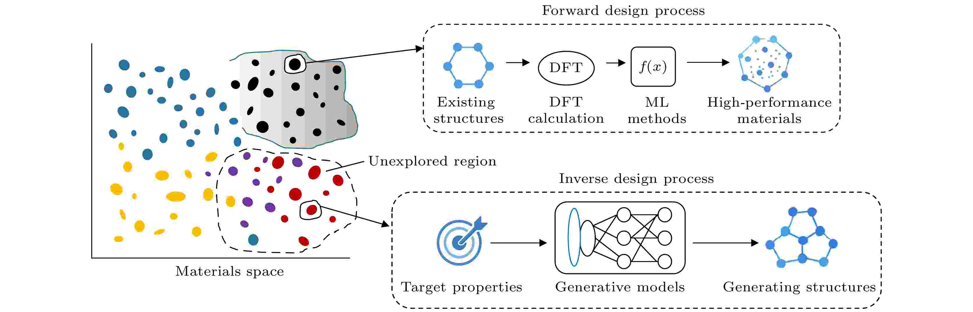
In recent years, the application of machine learning in materials science has significantly accelerated the discovery of new materials. In particular, when combined with traditional methods such as first-principles calculations, machine learning models have proven effective in screening potential high-performance materials from existing databases. However, these methods are largely limited by the known chemical spaces, making it difficult to achieve the active design of novel material structures. To overcome this limitation, generative models have become a promising tool for inverse material design, providing new avenues for exploring unknown structures and property spaces. Although existing generative models have achieved initial progress in crystal structure generation, achieving property-guided material generation remains a significant challenge. In this review paper, we first introduce the representative generative models recently applied to materials generation, including CDVAE, MatGAN, and MatterGen, and analyzes their basic abilities and limitations in structural generation. We then focus on strategies for incorporating target properties into generative models to generate the property-guided structure. Specifically, we discuss four representative methods: Con-CDVAE based on target property vectors, SCIGEN with integrated structural constraints and guidance mechanisms, a fine-tuned version of MatterGen leveraging adapter-based property control, and a CDVAE latent space optimization strategy guided by property objectives. Finally, we summarize the key challenges faced by property-guided generative models and provide an outlook on future research directions. This review aims to offer researchers a systematic reference and inspiration for advancing property-driven generative approaches in material design and provides researchers with a systematic reference and insight into the advancement of property-driven generative methods for materials design.

SPECIAL TOPIC—Semiconductor physics and devices
EDITOR'S SUGGESTION
2025, 74 (24): 241302.
doi: 10.7498/aps.74.20251120
Abstract +
Luminescence and anisotropy in two-dimensional (2D) materials have important implications for both fundamental material physics and potential applications such as polarized light-emitting devices. However, many natural-occuring 2D materials typically exhibit either luminescence or anisotropy, but not both. In this work, we utilize van der Waals (vdW) engineering to construct a heterostructure (HS) with anisotropic luminescent properties, which is composed of isotropic monolayer (1L) MoS2 (with strong intrinsic luminescence) and low-symmetry NbIrTe4 (strong anisotropy without photoluminescence). Experimentally, we characterize the optical response of the HS by using angle-resolved PL spectroscopy. The results indicate that the intrinsic anisotropic potential field of NbIrTe4 at the interface effectively breaks the in-plane isotropic symmetry of MoS2, inducing a pronounced polarization-dependent emission of A and B excitons. The anisotropy ratio is enhanced to ~1.58, corresponding to a linear polarization degree of approximately 22%. This work provides new insights into 2D interfacial coupling and offers useful guidance for the design and engineering of next-generation high-performance, tunable polarized light-emitting devices.
SPECIAL TOPIC—Atomic, molecular and materials properties data
EDITOR'S SUGGESTION
2025, 74 (24): 243101.
doi: 10.7498/aps.74.20251230
Abstract +
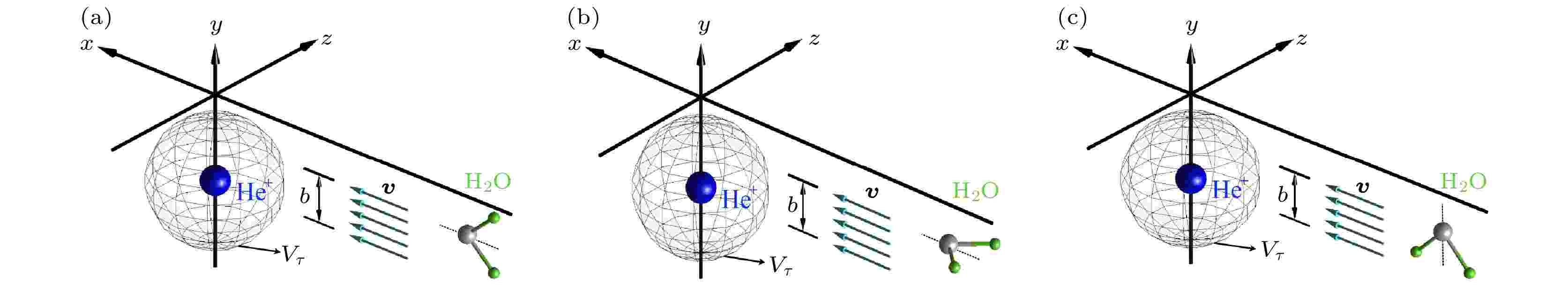
The charge transfer cross sections of collisions between He ions in the solar wind and H2O molecule constitute essential data required for the astrophysical plasma modeling. However, experimental measurements of single charge transfer (SCT) cross sections for He+-H2O collisions at low-to-intermediate energies (corresponding to the velocity range of the solar wind) are extremely scarce, and first-priciple theoretical calculations have not been conducted. In this study, employing the time-dependent density functional theory nonadiabatically coupled with the molecular dynamics, the SCT cross sections are calculated for He+-H2O collisions over a broad energy range of 1.33–1800 keV. An inverse collision framework is used to investigate the charge transfer dynamics and electron-ion coupling processes. It is found that the SCT cross section exhibits a strong dependence on the molecular orientation. Furthermore, there are significant differences in the contributions of different molecular orientations to the cross section between low-energy and high-energy regions. The computed cross section results show good agreement with the existing data obtained from experiments and classical theoretical models. This indicates that the present theoretical method and numerical framework are not only applicable to handling the charge transfer processes in collisions between dressed ions and molecules but also enable the quantitative analysis of the effect of molecular orientation on the cross section. This study lays a foundation for cross section calculations of complex collision systems. The datasets presented in this paper are openly available at https://doi.org/10.57760/sciencedb.j00213.00193 .
SPECIAL TOPIC—Atomic, molecular and materials properties data
EDITOR'S SUGGESTION
2025, 74 (24): 245101.
doi: 10.7498/aps.74.20250861
Abstract +
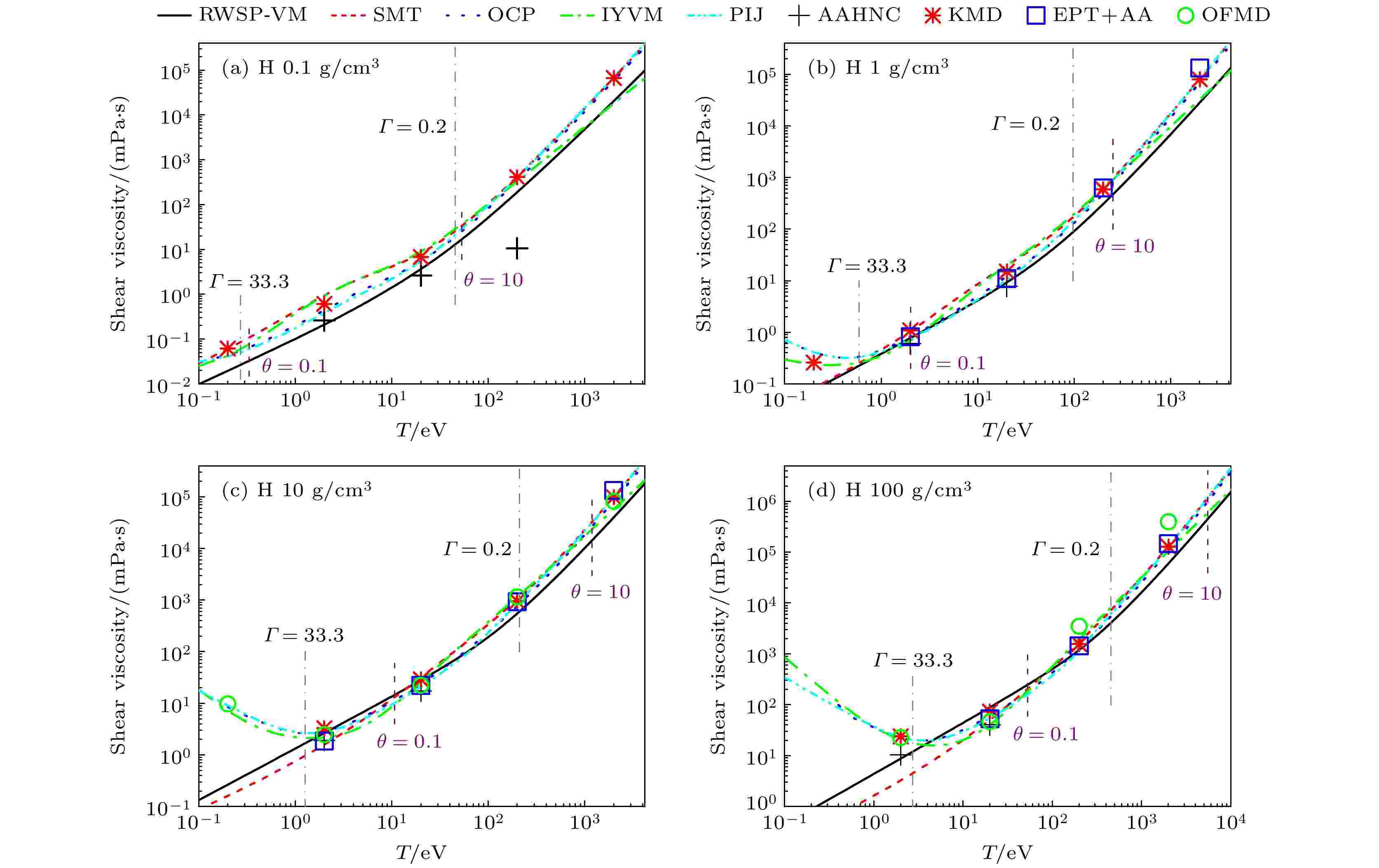
The viscosities of matters under extreme conditions, i.e. warm dense matter (WDM) and hot dense matter (HDM), have significant applications in various fields, such as the design of inertial confinement fusion targets, the astrophysical structure evolution, and the interfacial instability and mixing development under extreme conditions. Since the temperature and pressure ranges accessible by experimental techniques for viscosity measurement are very limited, the acquisition of viscosity data under extreme conditions mainly relies on theoretical calculations. This work introduces a variety of molecular dynamics (MD) methods and models for calculating the viscosities of WDM and HDM, they being quantum MD (QMD), orbital-free MD (OFMD), average atom model combined with hypernetted chain (AAHNC), effective potential theory combined with average atom model (EPT+AA), hybrid kinetics MD (KMD), integrated Yukawa viscosity model (IYVM), Stanton-Murillo transport model (SMT), pseudo-ion in jellium (PIJ), one-component plasma model (OCP), and random-walk shielding-potential viscosity model (RWSP-VM). Simultaneously, the viscosities of various elements obtained by these methods are shown, ranging from low to high atomic number (Z), i.e., H, C, Al, Fe, Ge, W, and U. The accuracy and the applicability of each method are analyzed in detail by comparison. RWSP-VM, which is based on physical modeling and independent of MD data, has comparable accuracy to simulation data over a wide range of temperature and pressure, and is an efficient method of obtaining viscosity data of WDM and HDM. This work will pave the way for calculating the shear viscosities under extreme conditions, and may play an important role in promoting the relevant applications. The data calculated from RWSP-VM in this work are openly available at https://doi.org/10.57760/sciencedb.j00213.00180 .
SPECIAL TOPIC—Atomic, molecular and materials properties data
EDITOR'S SUGGESTION
2025, 74 (24): 246201.
doi: 10.7498/aps.74.20251058
Abstract +
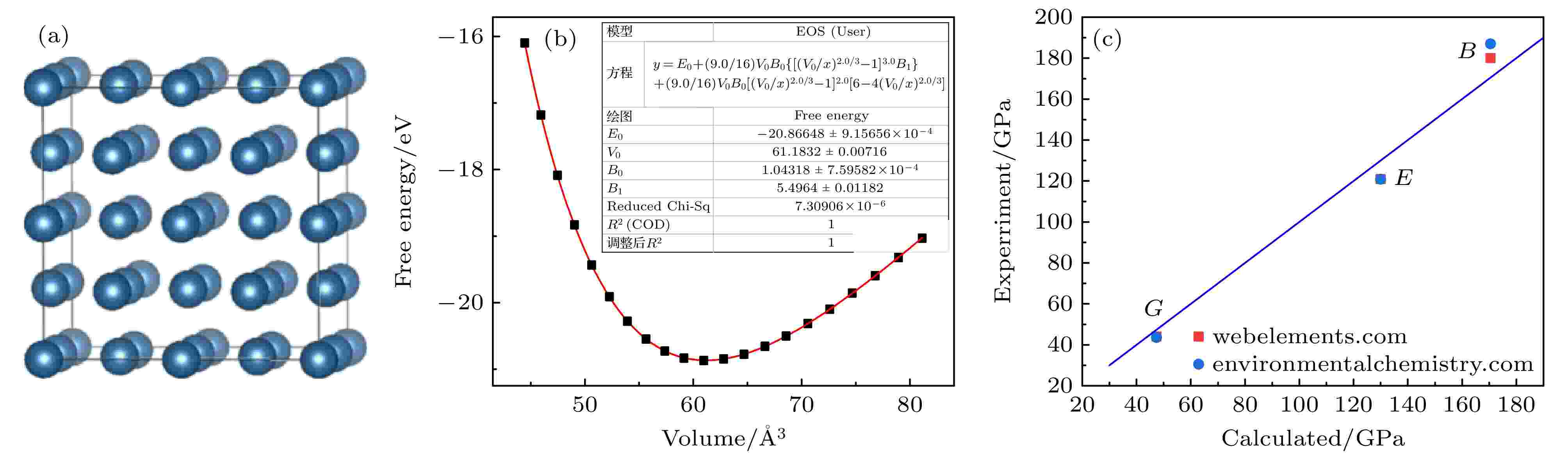
The lower friction coefficient and superior mechanical properties of palladium (Pd) alloys make them potentially advantageous for use in high-precision instruments and devices that require long-term stable performance. However, the high cost of raw materials and experimental expenses result in a lack of fundamental data, which hinders the design of high-performance Pd alloys. Therefore, in this study, first-principles calculations are used to determine the lattice constant and elastic modulus of Pd. A model of dilute solid solutions formed by Pd with 33 alloying elements including Al, Si, Sc, Ti, V, Cr, Mn, Fe, Co, Ni, and others, is established. The mixing enthalpy, elastic constant, and elastic modulus are calculated. The results show that, all other alloying elements except for Mn, Fe, Co, Ni, Ru, Rh, Os, and Ir can form solid solutions with Pd. Alloying elements from both sides of the periodic table enhance the ductility of Pd solid solutions, with La, Ag, and Zn having the most significant effects, while Cu and Hf reduce the ductility of Pd. Differential charge density analysis indicates that the electron cloud formed after doping with Ag is spherically distributed, thereby improving ductility. After doping with Hf, the degree of delocalization around the atoms is maximized, indicating a strong ionic bond between Hf and Pd, which results in a higher hardness of Pd31Hf. The datasets presented in this paper are openly available at https://www.doi.org/10.57760/sciencedb.j00213.00186 .
SPECIAL TOPIC—Instrumentation and metrology for ultrafast atomic and molecular spectroscopy
EDITOR'S SUGGESTION
2025, 74 (24): 243202.
doi: 10.7498/aps.74.20251166
Abstract +
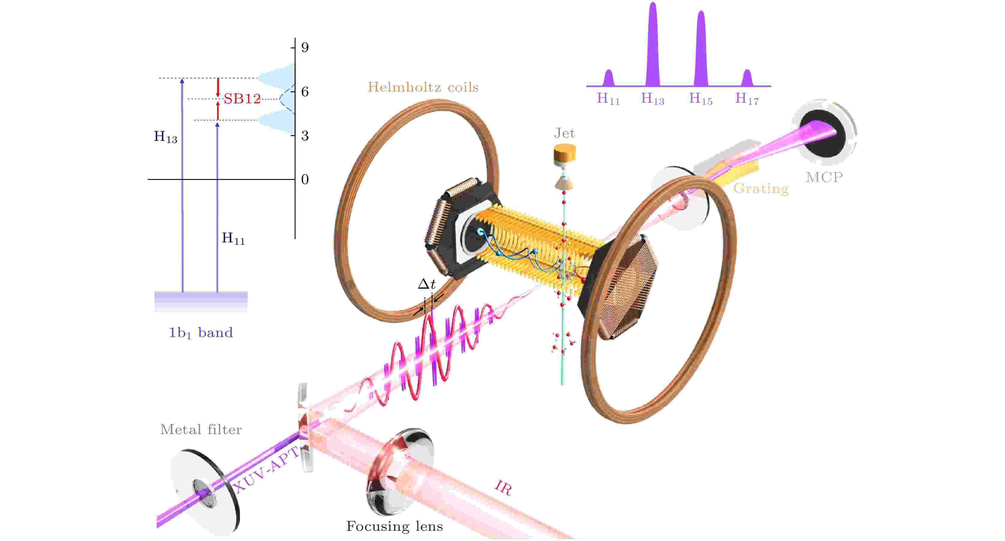
The evolution mechanisms of electrons in isolated atoms, molecules and complex systems on a natural time-scale have long been a fundamental question in atomic and molecular physics, with significant implications for the applications of quantum materials. Over the past two decades, the development of attosecond light pulses and attosecond metrology has opened new opportunities for investigating the electronic dynamics, while also posing new challenges. Traditional detection techniques, such as time-of-flight and velocity map imaging spectrometers, can be used to study the attosecond scattering phase shifts in the photoemission and ionization processes with extremely high temporal and energy resolution. However, the limitations in multi-particle coincidence detection and three-dimensional momentum correlation limit the deeper exploration of many-body correlations and non-adiabatic ultrafast dynamics involving electron-nuclear coupling. To enable multidimensional and real-time observation of the three-dimensional momenta of both electrons and ions during photoionization, the attosecond interferometry has been integrated into electron-ion coincidence systems. In this study, we utilize an attosecond coincidence interferometer that combines an attosecond pump-infrared femtosecond probe scheme with cold target recoil ion momentum spectroscopy. The apparatus enables attosecond-time-resolved momentum imaging of all charged fragments in atomic and molecular systems, thereby providing deeper insights into the dynamics of photoionization. We also highlight the recent groundbreaking applications and advances of attosecond coincidence interferometer in studying photoionization dynamics in atoms, molecules, and more complex systems.

SPECIAL TOPIC—Instrumentation and metrology for ultrafast atomic and molecular spectroscopy
EDITOR'S SUGGESTION
2025, 74 (24): 243203.
doi: 10.7498/aps.74.20251176
Abstract +
SPECIAL TOPIC—Instrumentation and metrology for ultrafast atomic and molecular spectroscopy
EDITOR'S SUGGESTION
2025, 74 (24): 244204.
doi: 10.7498/aps.74.20251130
Abstract +
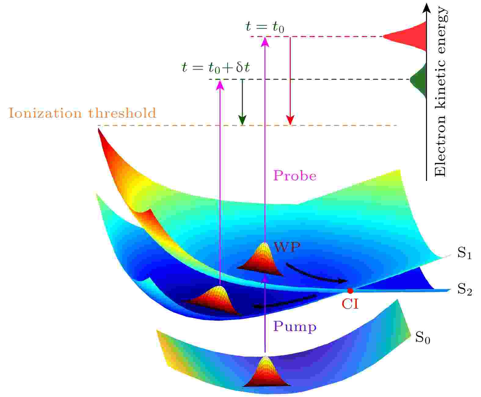
The liquid phase serves as a critical environment for chemical and biological reactions. The chemical and biological reaction dynamics of molecules in liquids exhibit evolution behaviors that are significantly different from those of isolated molecules in the gas phase. The in-depth investigation of the ultrafast excited-state dynamics of liquid-phase molecules is of great importance for uncovering the microscopic mechanisms underlying complex chemical and biological processes. Photoelectron spectroscopy not only reveals the electronic structure of excited-state molecules but also exhibits high sensitivity to structural changes, making it a powerful tool for studying the relaxation dynamics. Liquid-phase time-resolved photoelectron spectroscopy utilizes a liquid microjet within a high vacuum. In this pump-probe technique, an initial pump pulse excites the liquids to initiate dynamics, followed by a delayed probe pulse that ionizes the evolving system. The time-dependent energy distribution of the resulting photoelectrons, which encodes the ultrafast dynamics, is measured by a magnetic-bottle time-of-flight (MB-TOF) analyzer. This review systematically summarizes recent advancements in the time-resolved liquid-phase photoelectron spectroscopy technology for studying ultrafast dynamics in liquids, detailing the fundamental working principles of magnetic-bottle spectrometers and the preparation techniques for liquid microjet targets. Furthermore, typical applications are discussed, concluding with an analysis of current technical challenges and future research directions.

EDITOR'S SUGGESTION
2025, 74 (24): 244206.
doi: 10.7498/aps.74.20251069
Abstract +
Multiphoton microscopy (MPM) has become an essential research tool in biomedicine. Current MPM systems predominantly rely on Ti:sapphire lasers provided tunable femtosecond pulses at 720–950 nm. To access the second biological transparency window (1000–1350 nm), complex optical parametric oscillators are typically required. Furthermore, sources operating in the third biological transparency window (1600–1750 nm) are attracting significant attention for enhanced imaging depth. However, no ultrafast laser source simultaneously covering all three transparency windows exists, thus hindering the widespread application of MPM in life sciences. Here, we demonstrate a fiber-laser-based ultrafast source that generates four-color tunable pulses across 800–1650 nm, covering the full spectral range for multiphoton excitation. This source utilizes our proposed spectral selection technique via self-phase modulation (SESS). SESS ensures SPM-dominated spectral broadening, producing isolated spectral lobes. Filtering the outermost lobes will generate near-transform-limited pulses with broad wavelength tunability. Using this supercontinuum excitation source, we successfully realize label-free imaging of diverse biomedical specimens, validating the performance of MPM empowered by this novel driving source.

- 1
- 2
- 3
- 4
- 5
- ...
- 214
- 215


