SPECIAL TOPIC—Toward making functional devices at an atomic scale: Funda mentals and frontiers
IVITED REVIEW
INVITED REVIEW
2021, 70 (2): 027201.
doi: 10.7498/aps.70.20200914
Abstract +
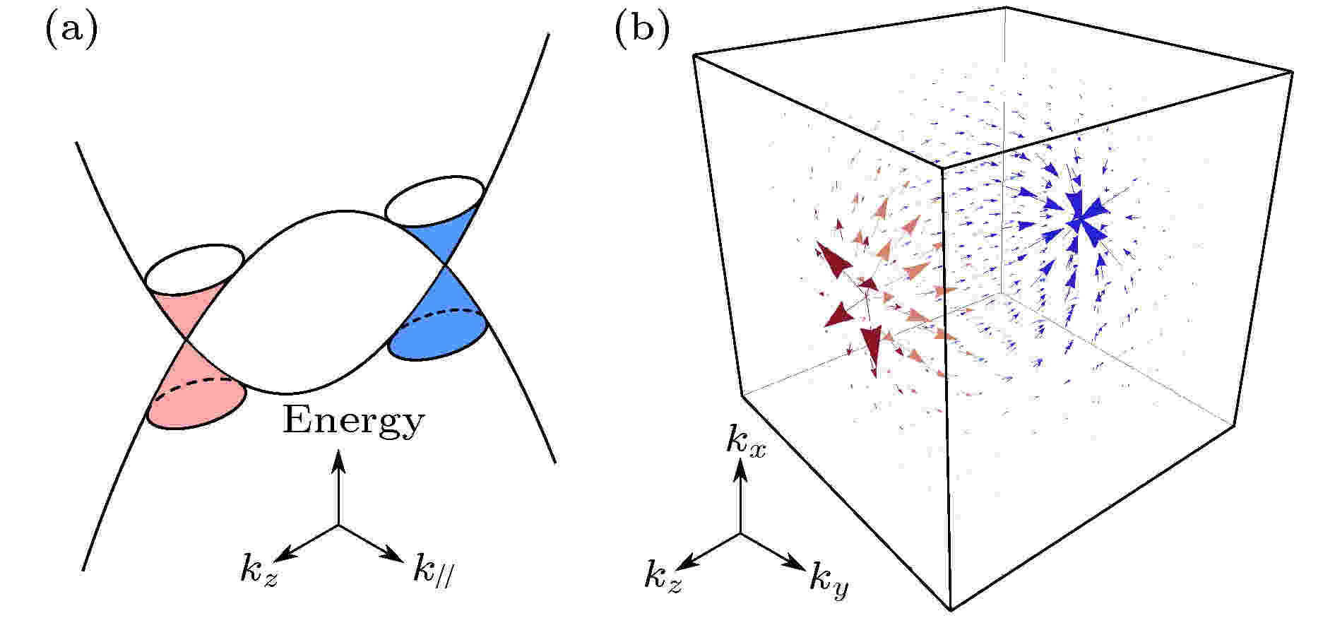
Topological matters include topological insulator, topological semimetal and topological superconductor. The topological semimetals are three-dimensional topological states of matter with gapless electronic excitations. They are simply divided into Weyl, Dirac, and nodal-line semimetals according to the touch type of the conduction band and the valence band. Their characteristic electronic structures lead to topologically protected surface states at certain surfaces, corresponding to the novel transport properties. We review our recent works on quantum transport mainly in topological semimetals. The main theories describing the transport behavior of topological matters are given in different magnetic regions.
SPECIAL TOPIC—Toward making functional devices at an atomic scale: Fundamentals and frontiers

EDITOR'S SUGGESTION
2021, 70 (2): 020701.
doi: 10.7498/aps.70.20201501
Abstract +
The atom manipulation technique based on scanning tunneling microscope refers to a method of relocating single atoms or molecules on a certain surface at atomic accuracy by using an atomically sharp tip, which is a unique and powerful tool for studying the quantum physics and prototype quantum devices on a nanometer scale. This technique allows us to build artificial structure atom-by-atom, thus some desired interesting quantum structures which are difficult to grow or fabricate by conventional methods could be realized, and unique quantum states, spin order, band structure could be created by the fine tuning of the structural parameters like lattice constant, symmetry, periodicity, etc. Combined with nanosecond scale time domain electric measurement and autonomous control technique, the atom manipulation would be useful in exploring the atomic precision prototype quantum devices, and providing some valuable knowledge for future electronics. In this review, we introduce the atom manipulation technique and related milestone research achievements and latest progress of artificial quantum structures, including electronic lattices with exotic quantum states on Cu(111), quantum dots on III-V semiconductors, magnetic structures with tunable spin order, structures for quantum information storage and processing, prototype Boolean logic devices and single atom devices. The STM lithography and autonomous atom manipulation are discussed as well. With such improvements, this technique would play more important roles in developing the functional quantum devices in future.
2021, 70 (2): 023701.
doi: 10.7498/aps.70.20201561
Abstract +
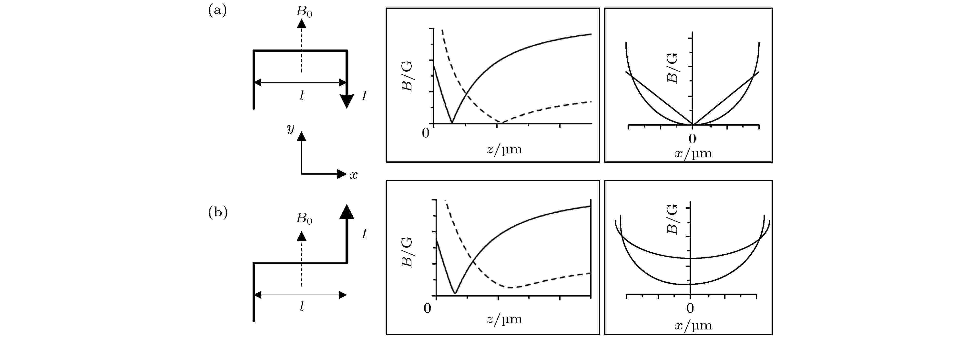
The laser cooling, trapping and manipulating of neutral atoms has become a valuable tool for scientists, providing innovative ways to probe the nature of reality and giving rise to transformative devices in the fields of precise measurement and quantum information processing. Unlike traditional complex and bulky atomic experimental facilities, atom chips, through the design, fabrication of surface-patterned microstructures, and the integration of devices on the substrates, can precisely control the magnetic, electric or optical fields on a micro-nano scale with low power consumption. It can realize strong trapping as well as coherent atomic manipulation. Since atom chip was first proposed twenty years ago, it has built a robust quantum platform for miniaturizing and integrating quantum optics and atomic physics tools on a chip. In this paper, first, we briefly review the development history of atom chips, then introduce the basic knowledge of micro potential traps and micro guides based on on-chip current-carrying wires. Afterwards, the key technologies about the chip material, design, fabrication, characterization and integration of atom chips are discussed in detail. We not only focus on the currently most active and successful areas - current carrying wires, but also look at more visionary approaches such as to the manipulation of atoms with real nano structures, say, carbon nano tubes. The design and fabrication principles of ideal atom chips are discussed as well. In the forth part, the worldwide plans and research projects involving with atom chip technologies are summarized, showing that many countries see this as an important foundational technology. Following that, the major developments in the application fields including atom clocks, atom interferometer gyroscope, cold atom gravimeter, etc are described. Finally, the challenges faced by atom chips towards practical application are pointed out and the prospects for their subsequent development are depicted.
2021, 70 (2): 024202.
doi: 10.7498/aps.70.20201537
Abstract +
2021, 70 (2): 026201.
doi: 10.7498/aps.70.20201437
Abstract +
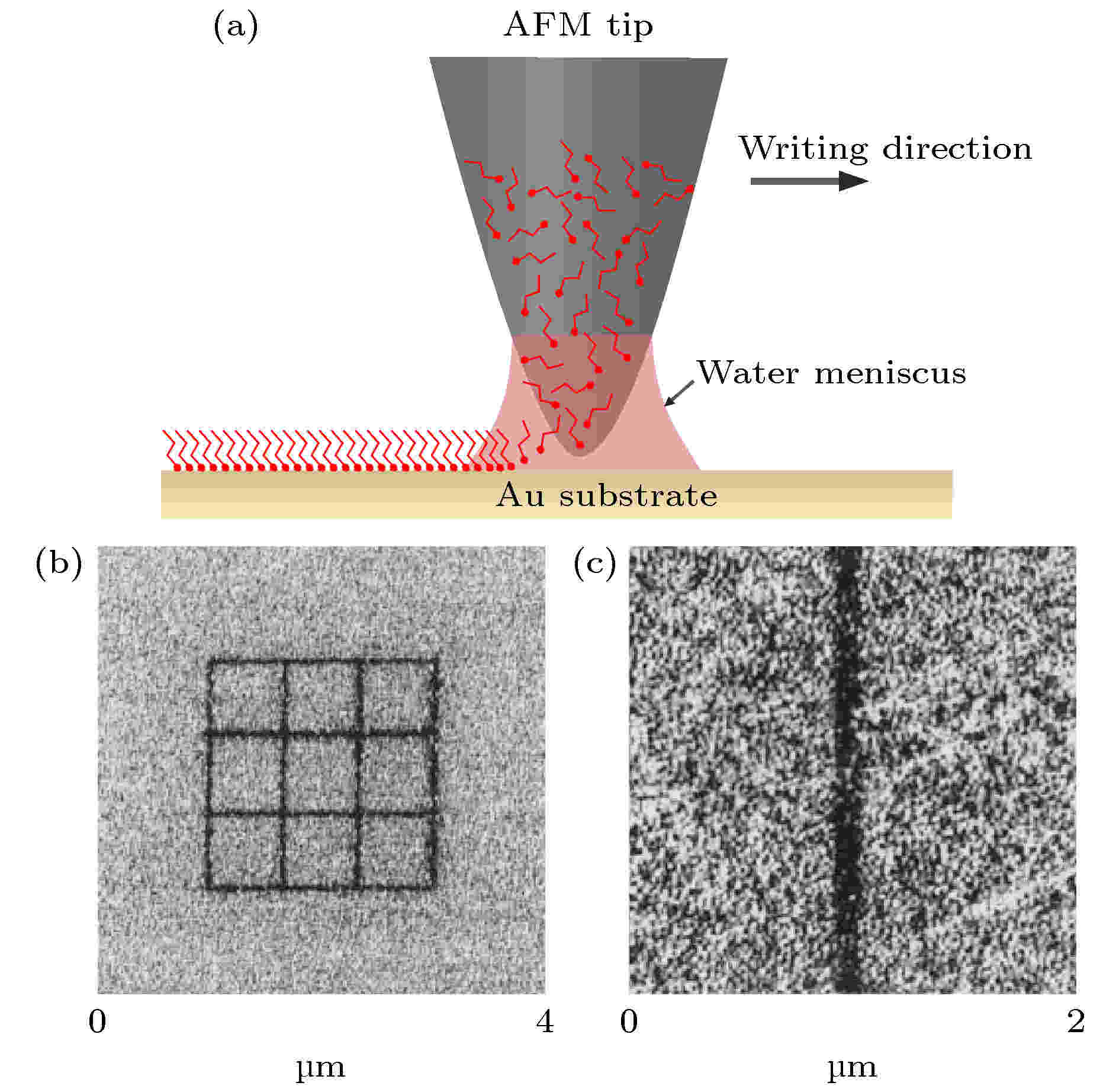
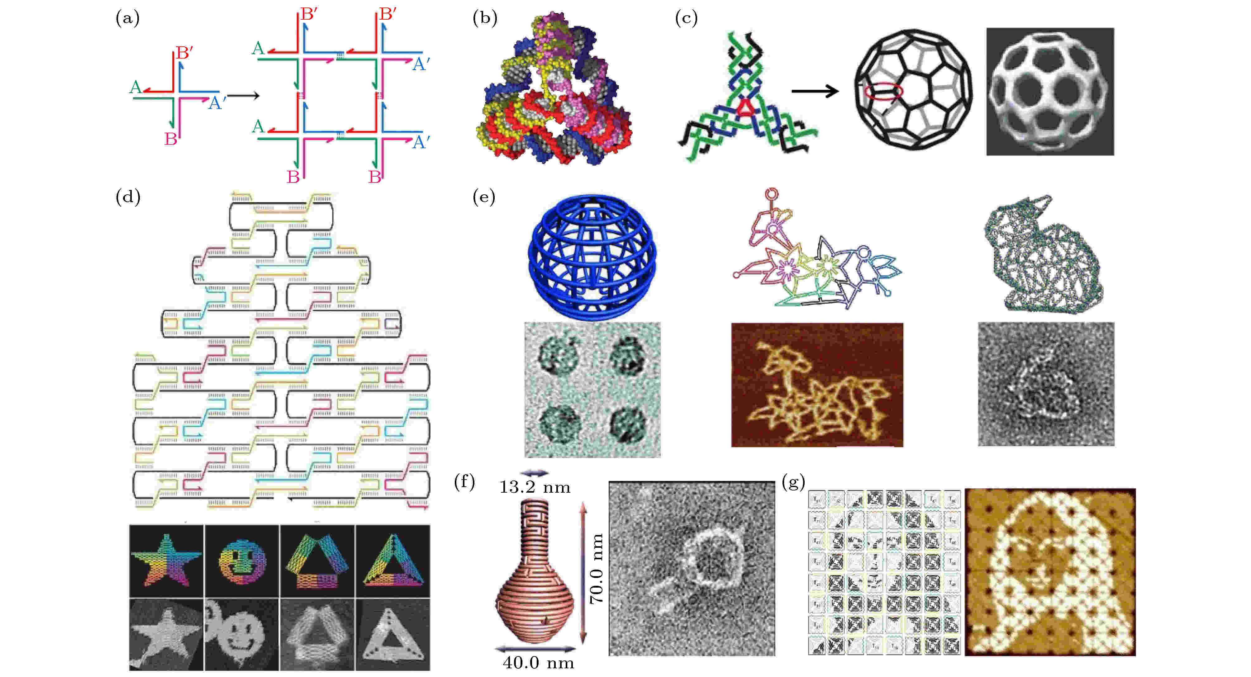
In recent years, the technology of traditional integrated circuit fabrication is facing a huge challenge. As the top-down lithography gradually approaches to its size limit, the development of atomic-scale precise fabrication for functional devices has already become a major scientific issue at present and might become a breakthrough in the development of information technology in the future. With the reference of the bottom-up self-assembly, which is the basic principle of constructing various advanced structures in living systems, the integrated assembly of atoms can be gradually constructed through a series of operations such as capturing, positioning, and moving atoms. The advent of framework nucleic acids (FNAs) happens to provide a new platform for manipulating single atom or integrating multiple atoms. As is well known, the nucleic acids are not only the carriers of genetic information, but also biological building blocks for constructing novel microscopic and macroscopic materials. The FNAs represent a new type of framework with special properties and features, constructed by nucleic acids’ bottom-up self-assembly. With the improvement of chemical synthesis and modification method of nucleic acids, various molecules and materials, such as fluorophores, nanoparticles, proteins, and lipids, can be spatially organized on FNAs with atomic precision, and these functionalized FNAs have been widely explored in the fields of biosensing, biocomputing, nano-imaging, information storage, nanodevices, etc. Based on the features of precise addressability, superior programmability and tailorable functionality, FNAs can be used for implementing the artificial self-assembly of objects with atomic precision to realize the precise arrangement in spatial and functional integration of basic assembly units, and even prompt the development of device fabrication from atomic scale to macroscopic scale. This review focuses on the intersection of FNAs and atomic fabrication, giving a systematically description of the feasibility and advantages of precisely atomic fabrication with FNAs from three aspects. First, the DNA/RNA nanoarchitectures from static state to dynamic state and general strategies for programmable functionalization of FNAs are briefly introduced. Then the applications of FNAs in device fabrication are highlighted, including single molecule reactors, single molecule sensors, nanodevices for cargo loading and transporting, nanophotonics, nanoelectronics and information processing devices. Finally, an outlook of the future development of atomic fabrication with FNAs is given as well.
2021, 70 (2): 026801.
doi: 10.7498/aps.70.20201406
Abstract +
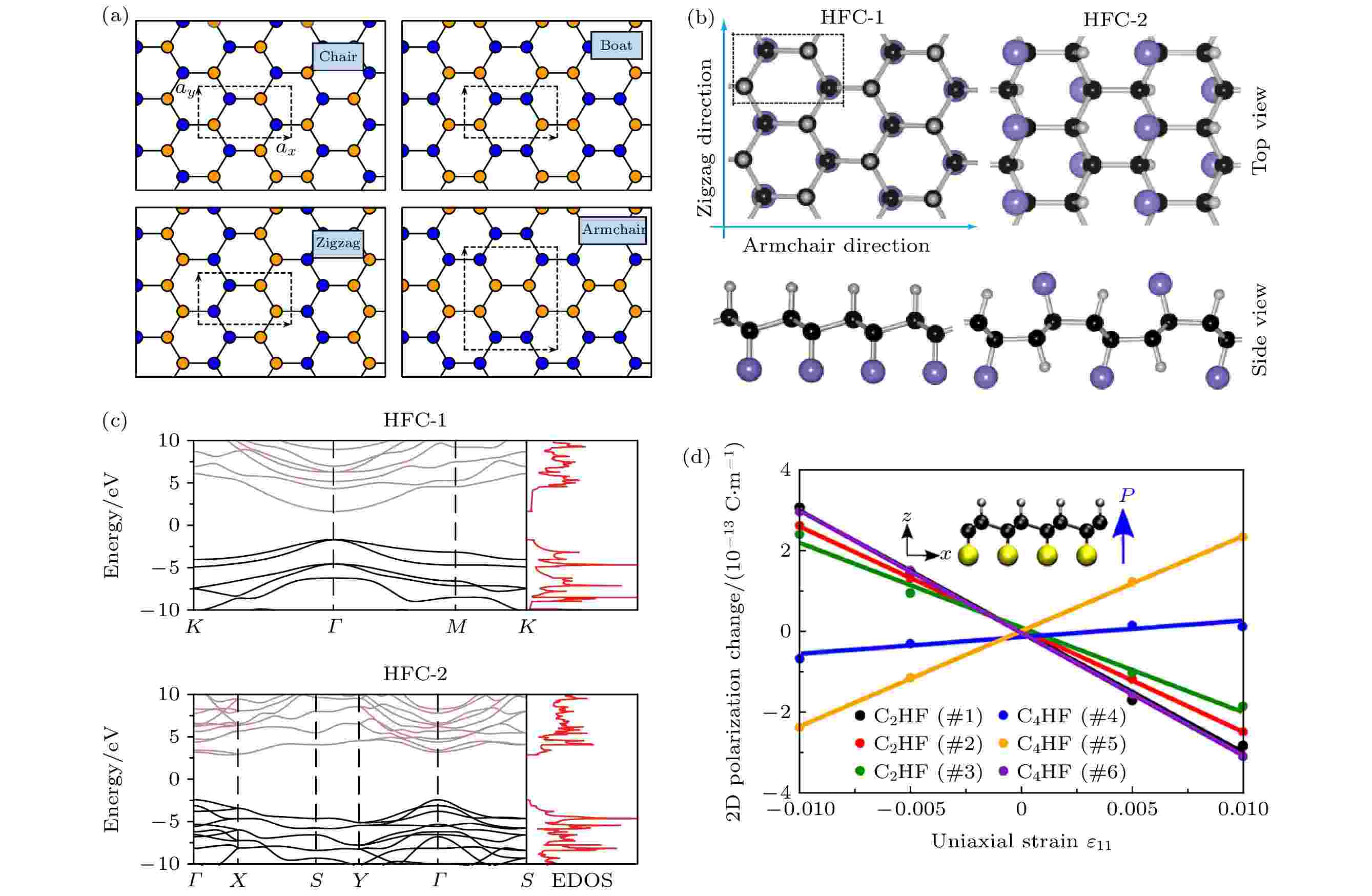
Since the advent of graphene, two-dimensional materials with various novel properties have received more and more attention in the fields of optoelectronic devices, spintronics and valley electronic devices. Among them, the excellent properties that appear in graphene with various molecular groups for asymmetric functionalization have led to the research of other Janus two-dimensional materials with asymmetric surface characteristics. As an important derivative of two-dimensional materials, Janus two-dimensional materials (especially Janus transition metal chalcogenides) have become a research hotspot in recent years. Both experiment and theory have confirmed that this kind of material has mirror asymmetry and novel characteristics, such as strong Rashba effect and out-of-plane piezoelectric polarization, and thus showing a great prospect for its applications in sensors, actuators, and other electromechanical devices. In this review we introduce the recent research progress of emerging Janus two-dimensional materials (including Janus graphene, various Janus two-dimensional materials and Janus two-dimensional van der Waals heterojunction), and summarize the unique electronic properties and potential applications of Janus two-dimensional materials. Finally, we draw some conclusions and depict a prospect of further exploration of Janus two-dimensional materials.
Chemical vapor deposition growth of large-areas two dimensional materials: Approaches and mechanisms
2021, 70 (2): 026802.
doi: 10.7498/aps.70.20201398
Abstract +
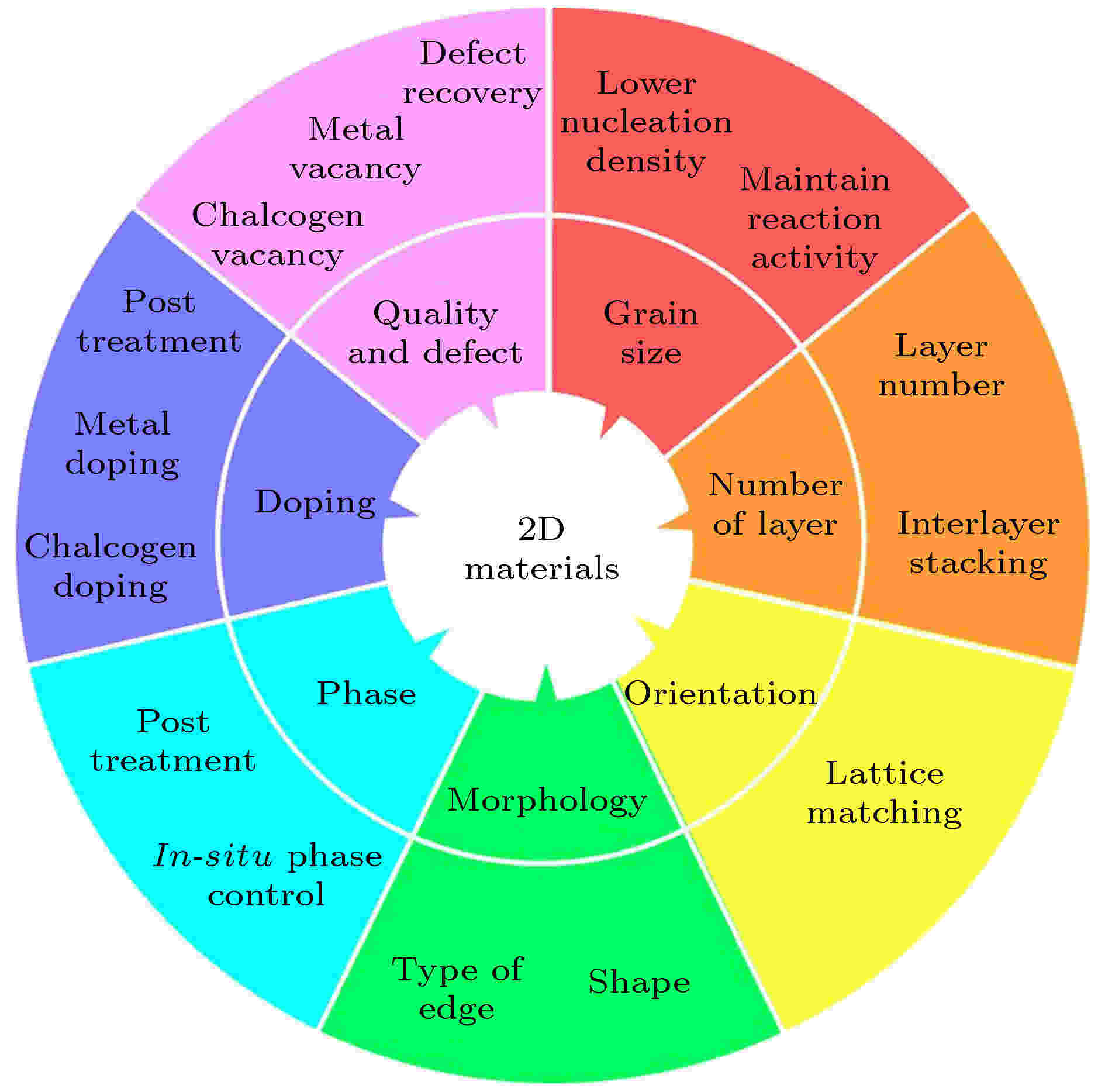
Two-dimensional (2D) layered materials have attracted increasing attention in recent years because of their abundant material categories and superior physical/chemical properties. In order to satisfy the requirements for highly integrated devices in the post-Moore era, substantial efforts have been devoted to producing atomically thin 2D materials with large lateral dimensions and high crystalline quality. The controllable synthesis is the precondition of the implementation of large mass producing 2D material in industry. Chemical vapor deposition (CVD) is a powerful method widely used in the synthesis of 2D materials and their hybrid structures. However, it is still challengeable to flexibly and easily grow any 2D materials into large area. Therefore, a systematic understanding of the requirements for controllable growth of different 2D materials are desired. In this review article, we provide a comprehensive discussion on the influencing factors, material transport, nucleation and growth rate in the CVD growth process. Finally, the strategies to further improve the size and quality of 2D materials are prospected.
2021, 70 (2): 027301.
doi: 10.7498/aps.70.20201636
Abstract +
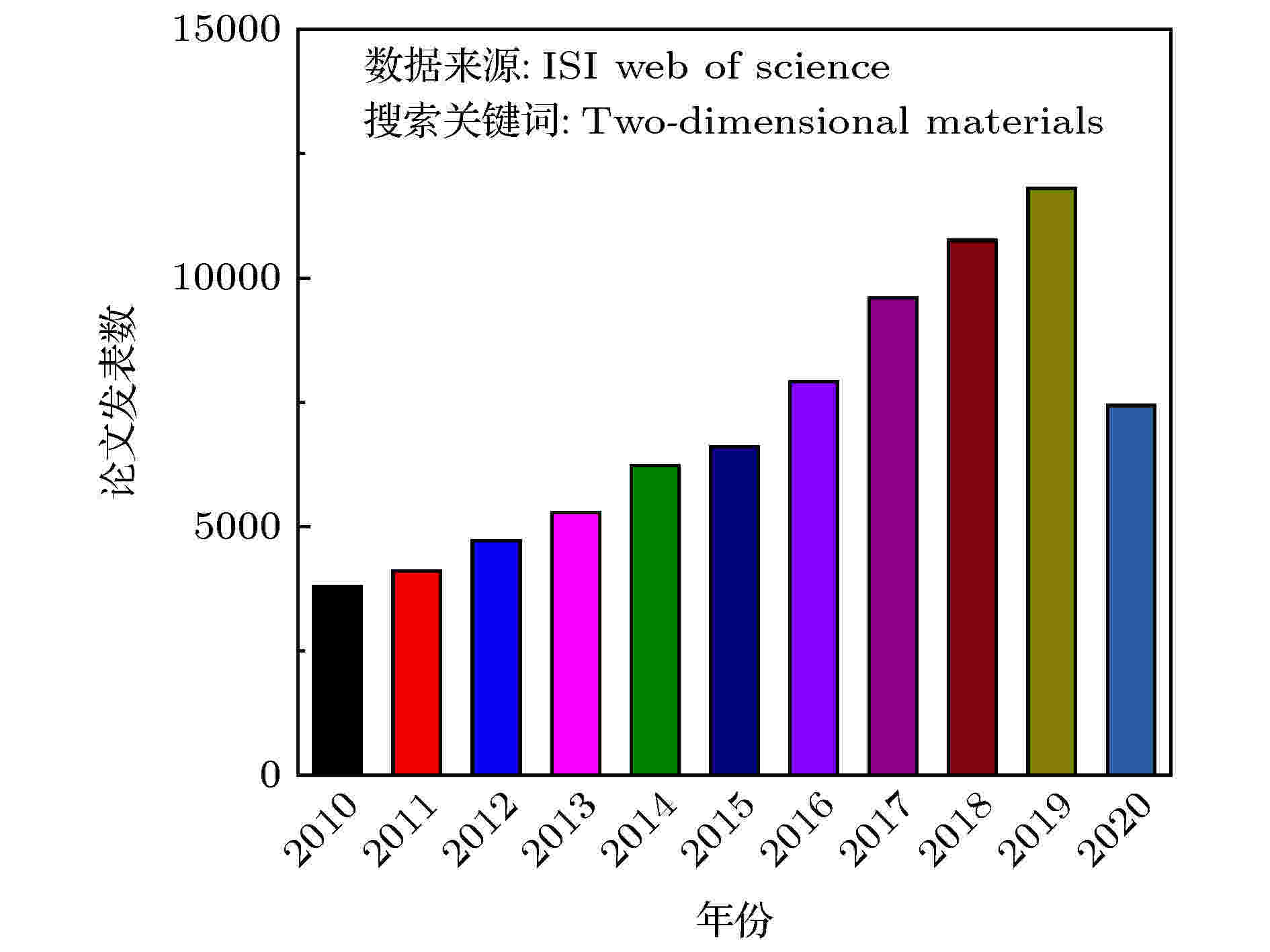
With the continuous development of information and technology, core components are developing rapidly toward faster running speed, lower energy consumption, and smaller size. Due to the quantum confinement effect, the continuous reduction of size makes materials and devices exhibit many exotic properties that are different from the properties of traditional three-dimensional materials. At an atomic scale level, structure and physical properties, accurately synthesizing, characterizing of materials, property regulation, and manufacturing of electronic devices with good performance all play important roles in developing the electronic devices and relevant applications in the future. Theoretical calculation can efficiently predict the geometric structure, physical properties and interface effects with low consumption but high accuracy. It is an indispensable research means of atomic level manufacturing technology. In this paper, we review the recent progress of two-dimensional materials from the theoretical perspective. This review is divided into three parts, i.e. two-dimensional layered materials, two-dimensional non-layered materials, and two-dimensional heterostructures. Finally, we draw some conclusions and suggest some areas for future investigation.
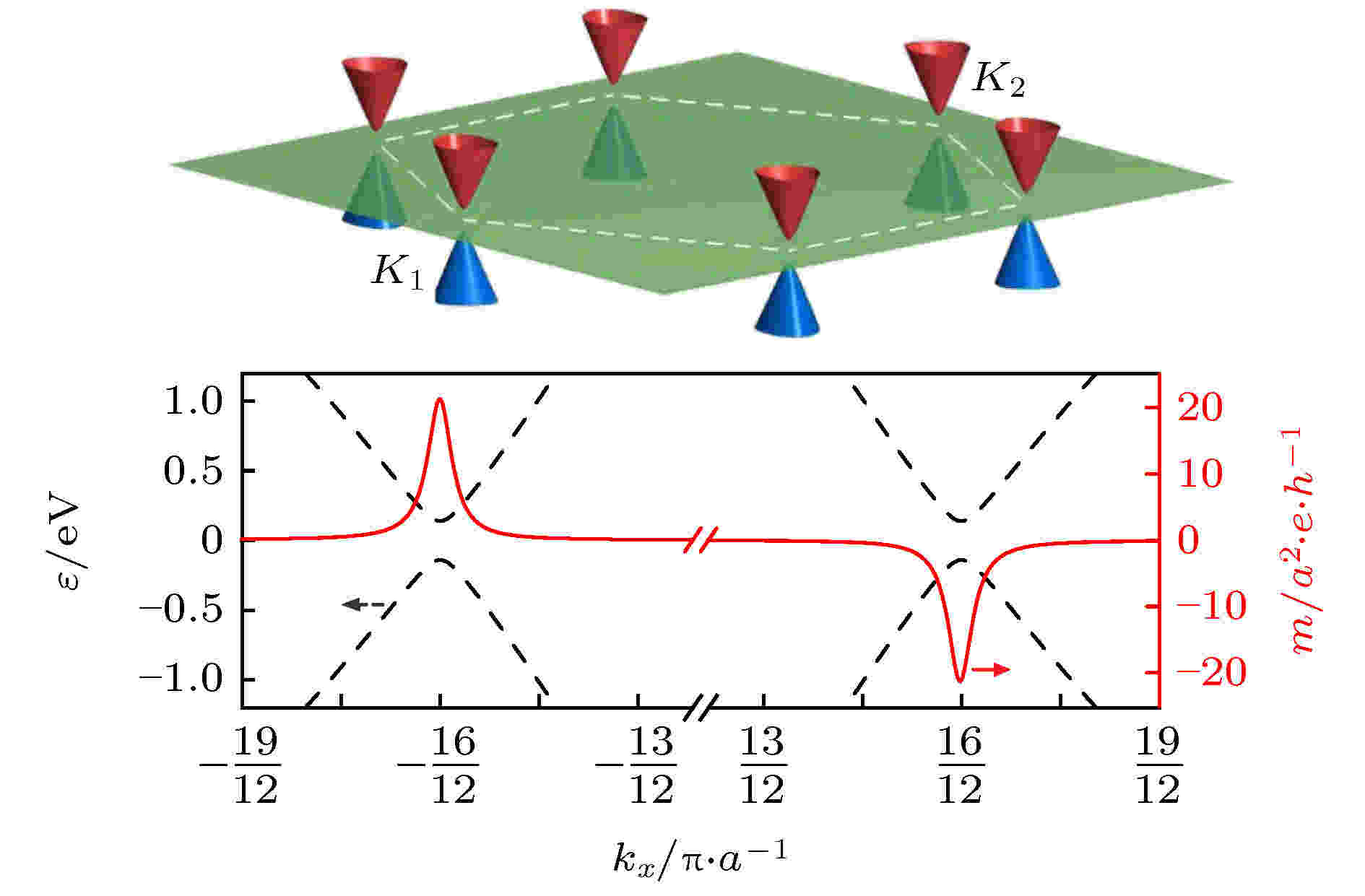
EDITOR'S SUGGESTION
2021, 70 (2): 027302.
doi: 10.7498/aps.70.20201415
Abstract +
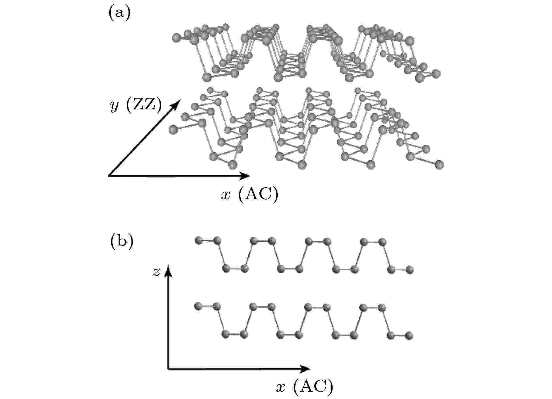
2021, 70 (2): 027802.
doi: 10.7498/aps.70.20201497
Abstract +
Recently, black phosphorus (BP), an emerging layered two-dimensional (2D) material, has aroused much research interest. Distinguished from most of other 2D materials, BP is always a direct bandgap semiconductor regardless of the thickness, with the bandgap ranging from 0.3 eV (bulk) to 1.7 eV (monolayer), which is just fill the gap in the bandgap between graphene and transition metal dichalcogenides (TMDCs) in this frequency range. Besides, the BP exhibits many intriguing properties, such as high carrier mobility, highly tunable and anisotropic physical properties, which render the BP another star 2D material following graphene and TMDCs. In this review, we mainly focus on the advances in the optical properties of 2D BP, with the content covering the intrinsic optical properties and external perturbation effects on optical properties. Regarding the intrinsic optical properties, we introduce the anisotropic and layer-dependent optical absorption from interband transitions, the layer-dependent exciton binding energy and exciton absorption, visible-to-infrared photoluminescence, and stability of absorption and photoluminescence. As for external perturbation effects on optical properties, we introduce in-plane uniaxial and biaxial strain effects, gate-induced quantum confined Franz-Keldysh effect and Burstein-Moss effect. And finally we give a brief summary and outlook, pointing out some several interesting and important issues of BP, which need further studying urgently such as hyperbolic plasmons, intersubband transitions, optical properties in heterostructures and twist angle moiré superlattice and so on. This review gives an overview of the optical properties of BP and is expected to arouse the interest in further studying the BP.
COVER ARTICLE
2021, 70 (2): 027901.
doi: 10.7498/aps.70.20201419
Abstract +
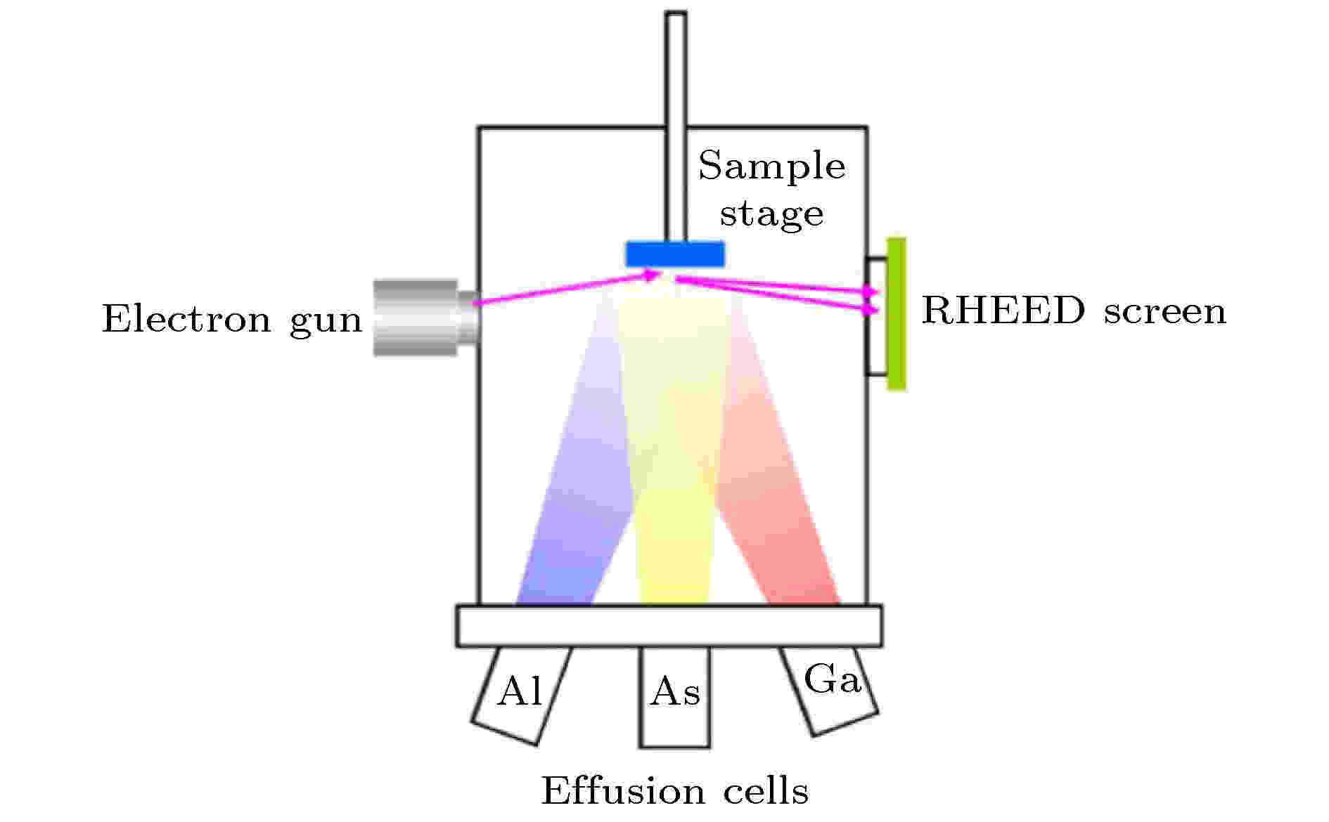
EDITOR'S SUGGESTION
2021, 70 (2): 028101.
doi: 10.7498/aps.70.20201436
Abstract +
With the development of future information devices towards smaller size, lower power consumption and higher performance, the size of materials used to build devices will be further reduced. Traditional “top-down” technology has encountered a bottleneck in the development of information devices on a nanoscale, while the vapor deposition technology has attracted great attention due to its ability to construct nanostructures on an atomic scale, and is considered to have the most potential to break through the existing manufacturing limits and build nano-structures directly with atoms as a “bottom-up” method. During molecular beam epitaxy, atoms and molecules of materials are deposited on the surface in an “atomic spray painting” way. By such a method, some graphene-like two-dimensional materials (e.g., silicene, germanene, stanene, borophene) have been fabricated with high quality and show many novel electronic properties, and the ultrathin films (several atomic layers) of other materials have been grown to achieve certain purposes, such as NaCl ultrathin layers for decoupling the interaction of metal substrate with the adsorbate. In an atomic layer deposition process, which can be regarded as a special modification of chemical vapor deposition, the film growth takes place in a cyclic manner. The self- limited chemical reactions are employed to insure that only one monolayer of precursor (A) molecules is adsorbed on the surface, and the subsequent self- limited reaction with the other precursor (B) allows only one monolayer of AB materials to be built. And the self- assembled monolayers composed of usually long- chain molecules can be introduced as the active or inactive layer for area- selective atomic layer deposition growth, which is very useful in fabricating nano- patterned structures. As the reverse process of atomic layer deposition, atomic-layer etching processes can remove certain materials in atomic precision. In this paper we briefly introduce the principles of the related technologies and their applications in the field of nano- electronic device processing and manufacturing, and find how to realize the precise control of the thickness and microstructure of functional materials on an atomic scale.
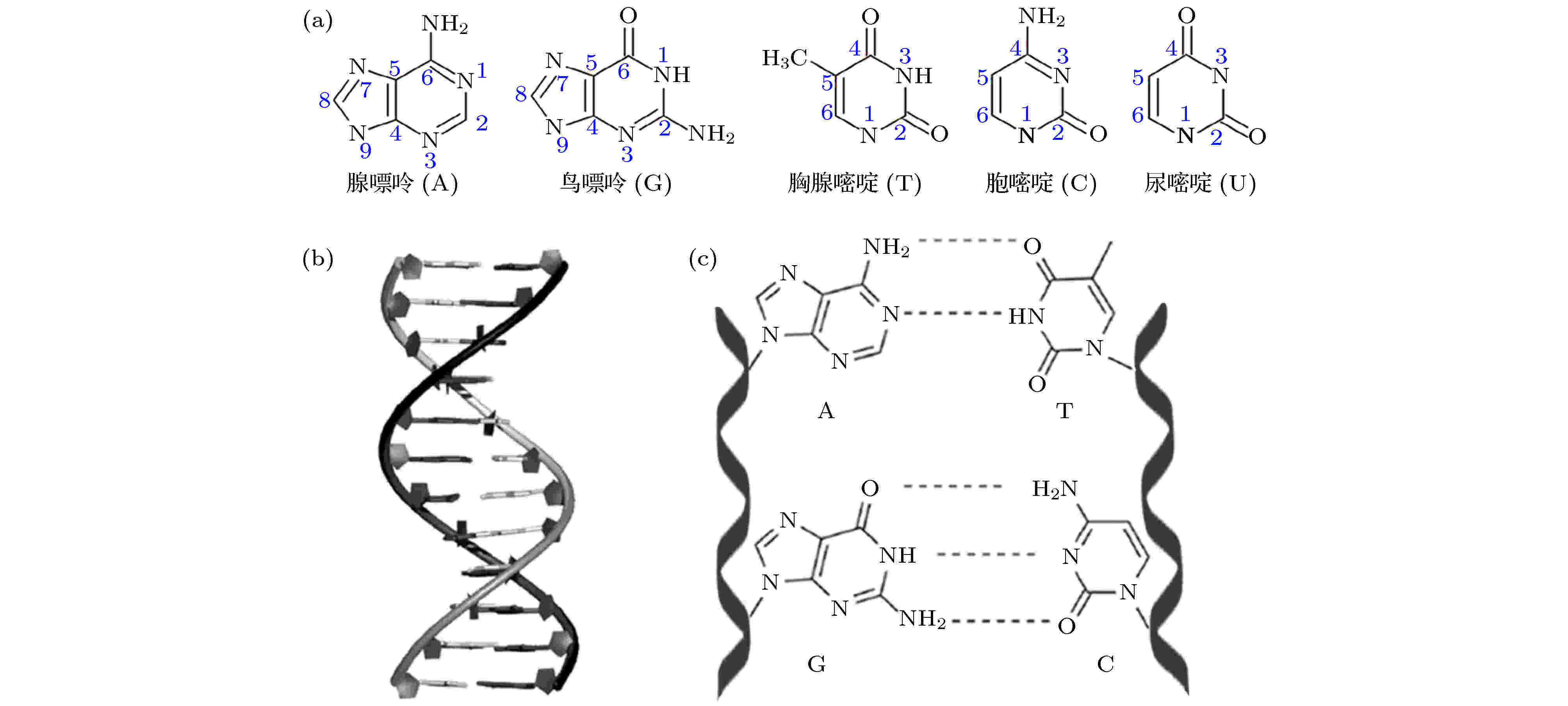
2021, 70 (2): 028102.
doi: 10.7498/aps.70.20201430
Abstract +
Atomic-scale and close-to-atomic scale manufacturing, a frontier hot issue in international academic research, is a cutting-edge manufacturing technique in which atoms are directly used as the manipulation object and atomic-scale structures with specific functions are established to meet the requirements for mass productions. This review focuses on precise atomic-scale manufacturing technology of nucleic acid materials. Firstly, the basic structures and functions of nucleic acid materials are introduced, and the basic principles of the interaction between DNA and metal atoms are discussed. Then the development process and breakthrough progress of nucleic acid materials-mediated precise atomic-scale manufacturing are introduced from the aspects of natural nucleic acid materials, artificial base “molecular elements”, and nucleic acid nanostructures. Finally, the challenges and opportunities in this field are systematically summarized and some suggestions for future development are given.
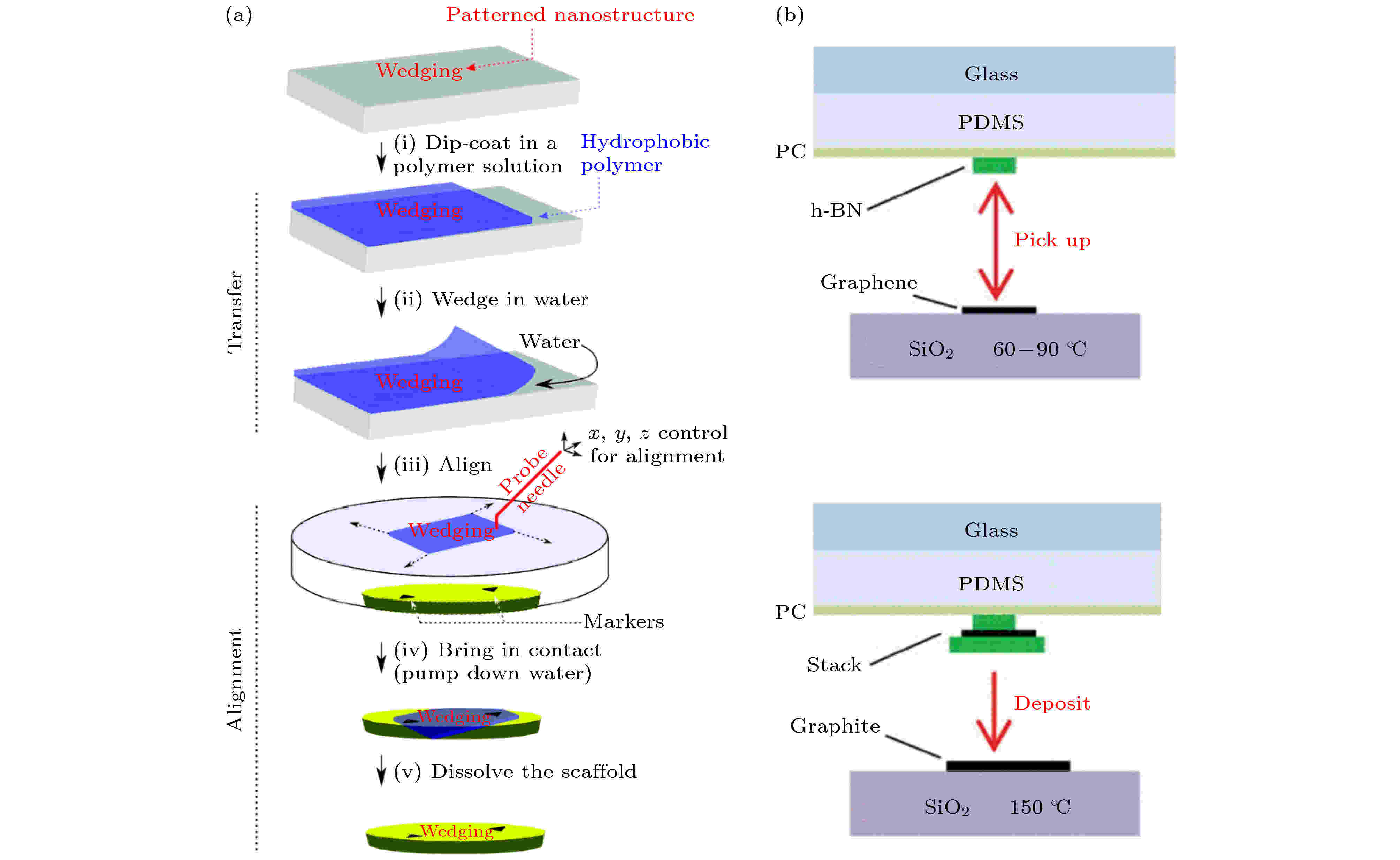
EDITOR'S SUGGESTION
2021, 70 (2): 028201.
doi: 10.7498/aps.70.20201425
Abstract +
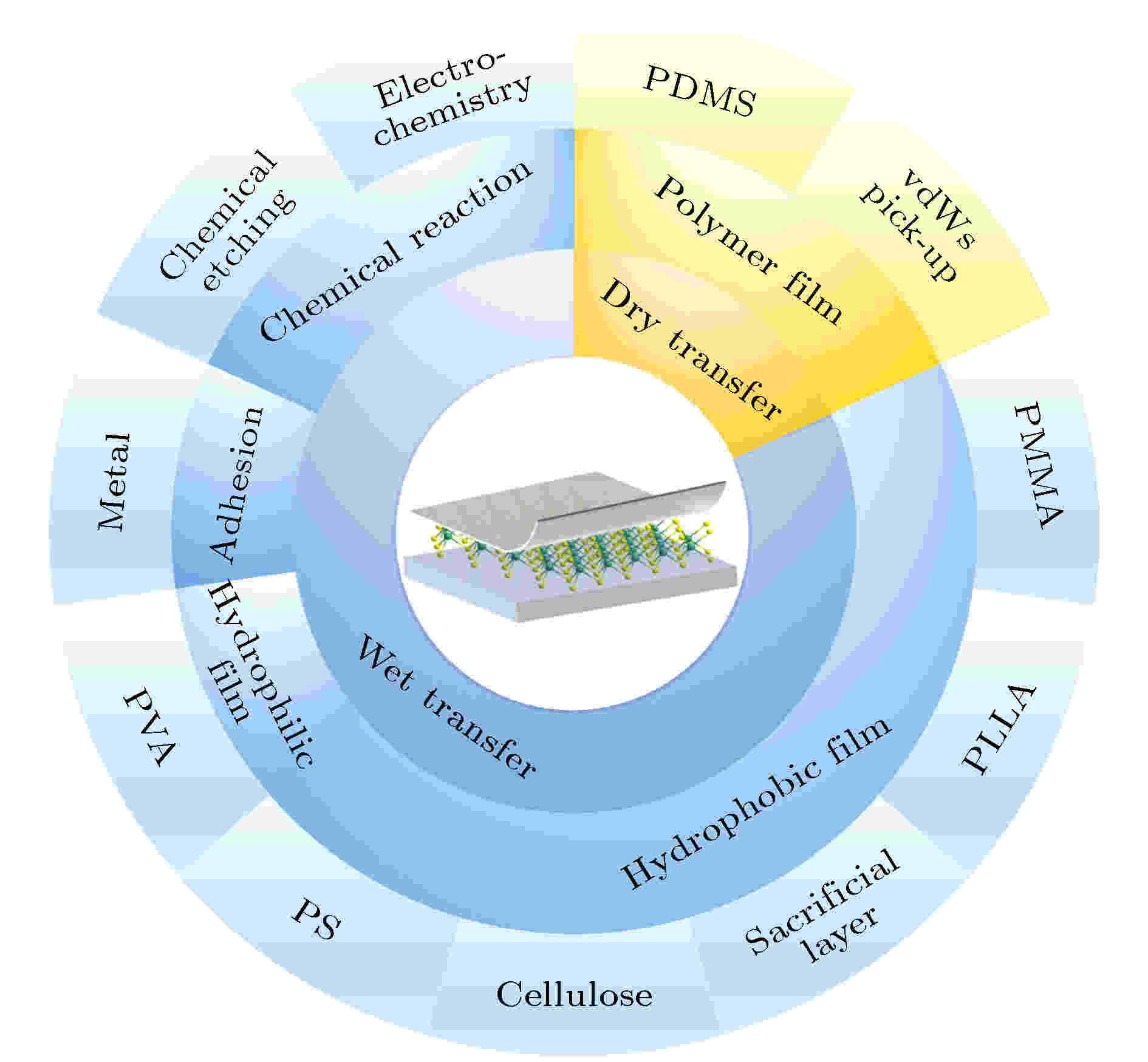
The advent of two-dimensional (2D) materials, a family of materials with atomic thickness and van der Waals (vdWs) interlayer interactions, offers a new opportunity for developing electronics and optoelectronics. For example, semiconducting 2D materials are promising candidates for extending the Moore's Law. Typical 2D materials, such as graphene, hexagonal boron nitride (h-BN), black phosphorus (BP), transition metal dichalcogenides (TMDs), and their heterostrcutures present unique properties, arousing worldwide interest. In this review the current progress of the state-of-the-art transfer methods for 2D materials and their heterostructures is summarized. The reported dry and wet transfer methods, with hydrophilic or hydrophobic polymer film assistance, are commonly used for physical stacking to prepare atomically sharp vdWs heterostructure with clear interfaces. Compared with the bottom-up synthesis of 2D heterostructures using molecular beam epitaxy (MBE) or chemical vapor deposition (CVD), the construction of 2D heterostructures by transfer methods can be implemented into a curved or uneven substrate which is suitable for pressure sensing, piezoelectric conversion as well as other physical properties’ research. Moreover, the transfer of 2D materials with inert gas protected or in vacuum operation can protect moisture-sensitive and oxygen-sensitive 2D materials from degerating and also yield interfaces with no impurities. The efficient and non-destructive large-area transfer technology provides a powerful technical guarantee for constructing the 2D heterostructures and exploring the intrinsic physical and chemical characteristics of materials. Further development of transfer technology can greatly facilitate the applications of 2D materials in high-temperature superconductors, topological insulators, low-energy devices, spin-valley polarization, twistronics, memristors, and other fields.
2021, 70 (2): 023601.
doi: 10.7498/aps.70.20201351
Abstract +
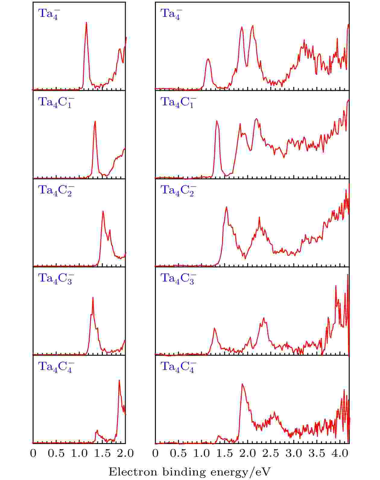
The electronic structures, chemical bonds and stabilities of ${\rm{Ta}}_4{\rm{C}}_n^{-/0} $ (n = 0–4) clusters are investigated by combining anion photoelectron spectroscopy with theoretical calculations. The vertical detachment energy values of ${\rm{Ta}}_4{\rm{C}}_n^{-} $ (n = 0–4) anions are measured to be (1.16 ± 0.08), (1.35 ± 0.08), (1.51 ± 0.08), (1.30 ± 0.08), and (1.86 ± 0.08) eV, and the electron affinities of neutral Ta4Cn (n = 0–4) are estimated to be (1.10 ± 0.08), (1.31 ± 0.08), (1.44 ± 0.08), (1.21 ± 0.08), and (1.80 ± 0.08) eV, respectively. It is found that the geometry structure of ${\rm{Ta}}_4^- $ cluster is a tetrahedron, and the most stable structure of ${\rm{Ta}}_4{\rm{C}}_1^{-} $ has a carbon atom capping one face of the ${\rm{Ta}}_4^- $ tetrahedron, while in the ground state structure of ${\rm{Ta}}_4{\rm{C}}_2^{-} $ cluster, two carbon atoms cap two faces of the${\rm{Ta}}_4^- $ tetrahedron, respectively. The lowest-lying isomer of ${\rm{Ta}}_4{\rm{C}}_3^{-} $ cluster holds a cube-cutting-angle structure. The ground state structure of ${\rm{Ta}}_4{\rm{C}}_4^{-} $ is a 2 × 2 × 2 cube. The neutral Ta4Cn (n = 0–4) clusters have similar structures to their anionic counterparts and the neutral Ta4C4 cluster can be considered as the smallest cell for α-TaC face-centered cube crystal. The analyses of molecular orbitals reveal that the SOMO of ${\rm{Ta}}_4{\rm{C}}_3^{-} $ is mainly localized on one tantalum atom, inducing a low VDE. Our results show that the Ta-Ta metal bonds are replaced by Ta-C covalent bonds gradually as the number of carbon atoms increases in ${\rm{Ta}}_4{\rm{C}}_n^{-/0} $ (n = 0–4) clusters. The per-atom binding energy values of ${\rm{Ta}}_4{\rm{C}}_n^{-/0} $ (n = 0–4) clusters are higher than those of ${\rm{Ta}}_{4+n}^{-/0} $ (n = 0–4) clusters, indicating that the formation of Ta-C covalent bonds may raise the melting point. The per-atom binding energy of neutral Ta4C4 is about 7.13 eV, which is quite high, which may contribute to the high melting point of α-TaC as an ultra-high temperature ceramic material.
2021, 70 (2): 027102.
doi: 10.7498/aps.70.20201434
Abstract +
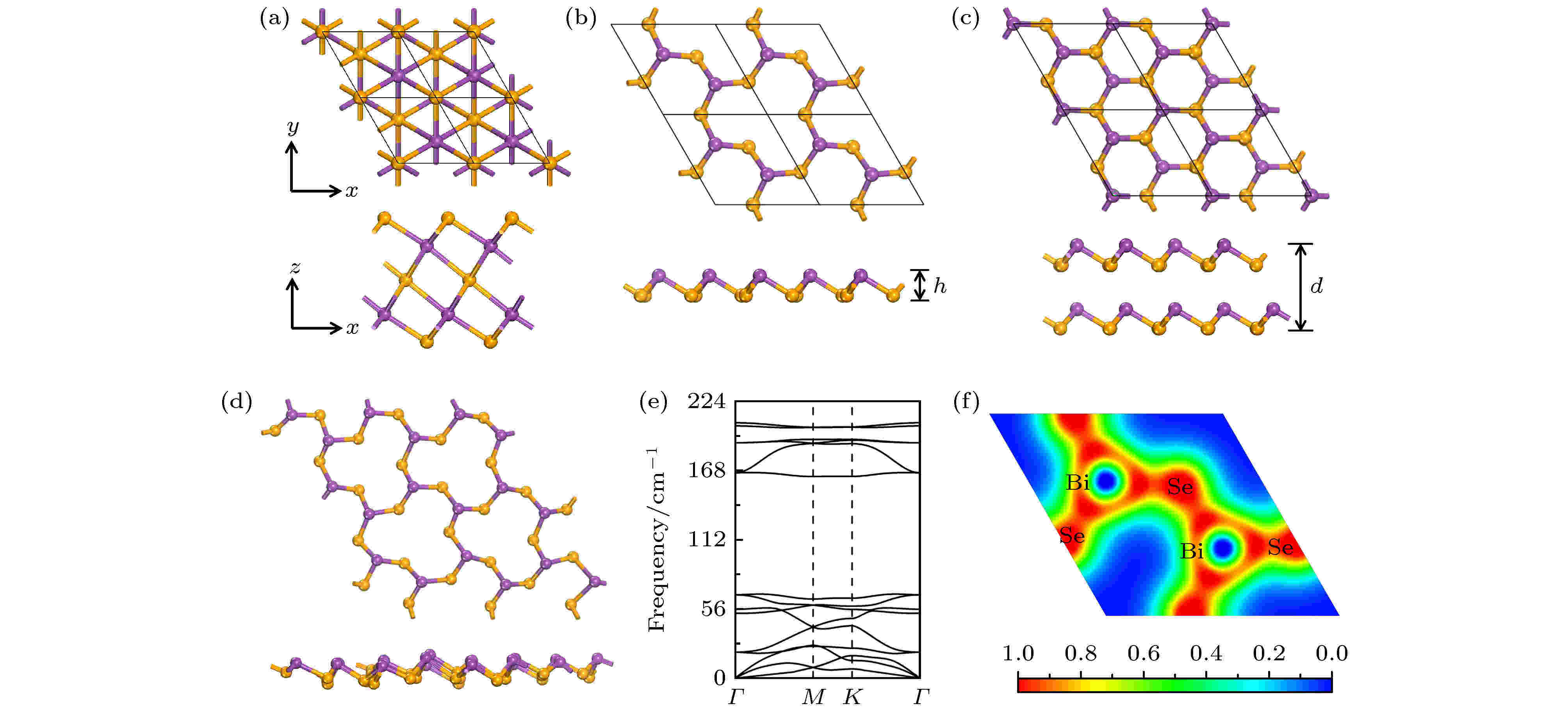
Recently, the boom of graphene has aroused great interest in searching for other two-dimensional (2D) compound materials, which possess many intriguing physical and chemical properties. Interestingly, 2D allotropes of differing atomic structures show even more diverse properties. The Bi2Se3 has attracted much attention due to its unique physical properties, while its allotrope has not been investigated. Based on first-principle calculations, here in this work we predict a new phase of Bi2Se3 monolayer with outstanding dynamic and thermal stabilities, named as β-Bi2Se3. Notably, the β-Bi2Se3 monolayer is a semiconductor with a modest direct band gap of 2.40 eV and small effective mass down to 0.52m0, large absorption coefficient of 105 cm–1 in the visible-light spectrum, suitable band edge positions for photocatalysis of water splitting. Moreover, the breaking of mirror symmetry in β-Bi2Se3 along the out-of-plane direction induces vertical dipolar polarization, yielding a remarkable out-of-plane piezoelectric coefficient of 0.58 pm/V. These exceptional physical properties render the layered Bi2Se3 a promising candidate for future high-speed electronics and optoelectronics.
REVIEW

2021, 70 (2): 027801.
doi: 10.7498/aps.70.20201325
Abstract +
In recent years, due to their unique physical, chemical and electronic properties, two-dimensional materials have received more and more researchers’ attention. In particular, the excellent optoelectronic properties and transport properties of two-dimensional materials such as graphene, black phosphorous and transition metal sulfide materials make them have broad application prospects in the field of next-generation optoelectronic devices. In this article, we will mainly introduce the advantages of two-dimensional materials in the field of photodetection, outline the basic principles and parameters of photodetectors, focus on the difference between the grating effect and the traditional photoconductive effect, and the reasons and characteristics of improving optical gain and optical responsivity. Then we review the latest developments and applications of grating local control in photodetectors, and finally summarize the problems faced by the photodetectors of this kind and their prospects for the future.

2021, 70 (2): 028402.
doi: 10.7498/aps.70.20201222
Abstract +
As one of the most dazzling star materials in recent years, perovskite has attracted extensive attention due to its unique photoelectric properties. Since the first report on 3.8% power conversion efficiency of perovskite solar cells (PSCs) was published in 2009, its efficiency has increased to 25.2% in a short period of 10 years, almost comparable to the efficiency of commercial polysilicon cells. However, due to its simple preparation process, it is easy to introduce a large number of defects in the film formation process. The defects accelerate the recombination of carriers and thus hindering the carrier transport channel, which is unfavorable for the preparation of high efficiency perovskite solar cells. Moreover, the existence of defects will affect the stability of PSCs, accelerate the degradation of materials, thereby hindering its further commercial development. Therefore, it is very important to understand the mechanism of defects and effectively suppress the generation of defects for the fabrication of high performance devices. As an effective passivation strategy, the interface modification has been widely used. In this paper, the locations of defects in different structures of devices and their effects on device performance are discussed. Based on the carrier transport layer passivation strategy and perovskite interface modification strategy, the mechanism of the passivation defects at the transport layer/perovskite interface is analyzed. The great advantages of passivation strategy and the classification of appropriate passivation materials are pointed out. It is hoped that this paper can provide useful guidance for developing the perovskite solar cells with high repeatability, high efficiency and long-term stability.
GENERAL

2021, 70 (2): 020301.
doi: 10.7498/aps.70.20200855
Abstract +
That the simultaneous quantum key distribution and classical communication (SQCC) scheme are combined with the continuous variable quantum key distribution (CVQKD) and the classical communication together, will provide an effective method to implement the simultaneous CVQKD and the classical communication in the existing optical networks in the future. However, superimposing a classical signal on the quantum signal will introduce excess noise into the CVQKD system, thus greatly reducing the performance of the system. In this paper, a novel scheme of SQCC based on optical preamplifier (OPA) is proposed, that is, the OPA is inserted into the receiver to improve the performance of the system. On the one hand, under the condition of the same bit error rate, the amplification of the signal by the OPA can reduce the requirement for the modulation amplitude of the classical signal at the sending end, thereby reducing the noise effect of the classical signal on the quantum signal. On the other hand, the OPA can compensate for the imperfection of the receiver detector. Moreover, in the case of locally generated local oscillator, the amplifier can also amplify the weak phase reference pulse, and thus reducing the phase excess noise caused by the shot noise of the weak phase reference pulse. Numerical simulation results show that the proposed scheme has better performance than the original scheme in the sense of security key rate and transmission distance. These results show that this scheme provides an effective and practical method for the further development and practical application of the SQCC scheme.
2021, 70 (2): 020501.
doi: 10.7498/aps.70.20200982
Abstract +
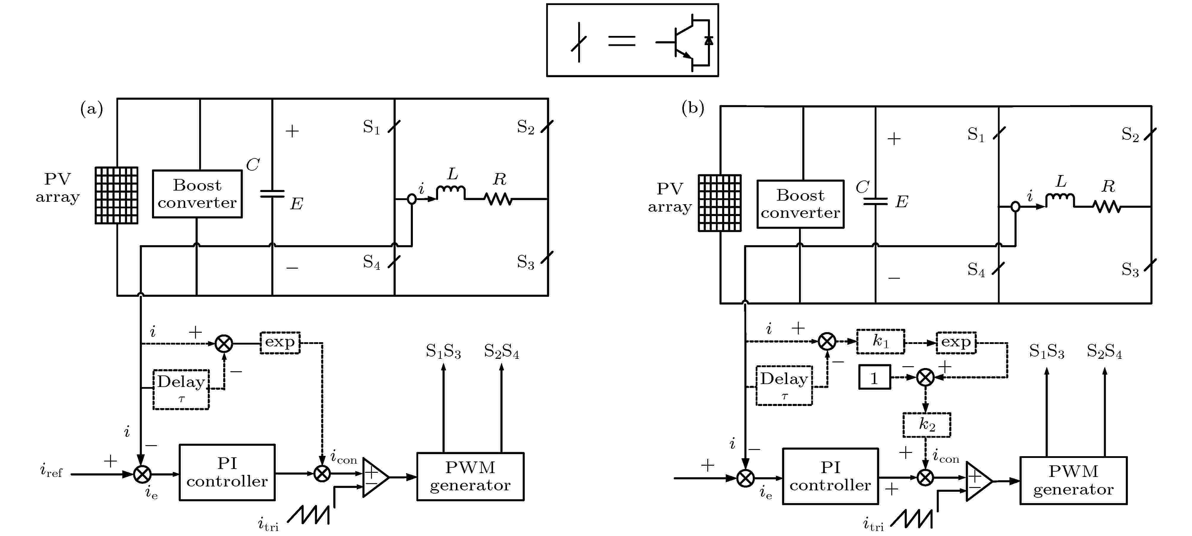
There are complex nonlinear behaviors such as bifurcation and chaos in a single-phase H-bridge photovoltaic inverter under proportional integral control, which will increase the harmonic content of the output current greatly and reduce the stability of system operation and reliability of power supply. There are the problems suffering the complicated modeling and difficulty in determining the control coefficients in existing chaos control methods. The exponential delay feedback control is a further development of the delay feedback control, which has the advantages of requiring no precise mathematical model of the system and simple implementation. However, our research shows that when the exponential delay feedback control is directly applied to the system, the feedback intensity cannot be controlled, which will bring too big a disturbance to the system. Based on it, an improved exponential delayed feedback control method is proposed in this paper. Firstly, a feedback signal is formed by the difference between the output current of the system and its own delay, then the feedback signal is used to obtain the control signal through an exponential link, a subtraction link and an proportion link, and the control signal is applied to the controlled system in the form of a feedback. At the same time, the discrete mapping model of the system is established and its Jacobian matrix expression is determined. Finally, the limiting conditions of the feedback control coefficient of the control signal are derived based on the stability criterion, and the control is applied to the system. In order to verify the control effect of this method, a lot of simulation experiments are conducted. The results show that the problems that the exponential delay feedback cannot control the feedback strength and causes excessive disturbance to the system will be effectively solved by this method. When the bifurcation parameters vary greatly, the chaos behaviors in the system will be suppressed effectively, the stable operating domain of the system will be expanded greatly and the harmonic content of the output current will be reduced.
NUCLEAR PHYSICS
2021, 70 (2): 022901.
doi: 10.7498/aps.70.20201141
Abstract +
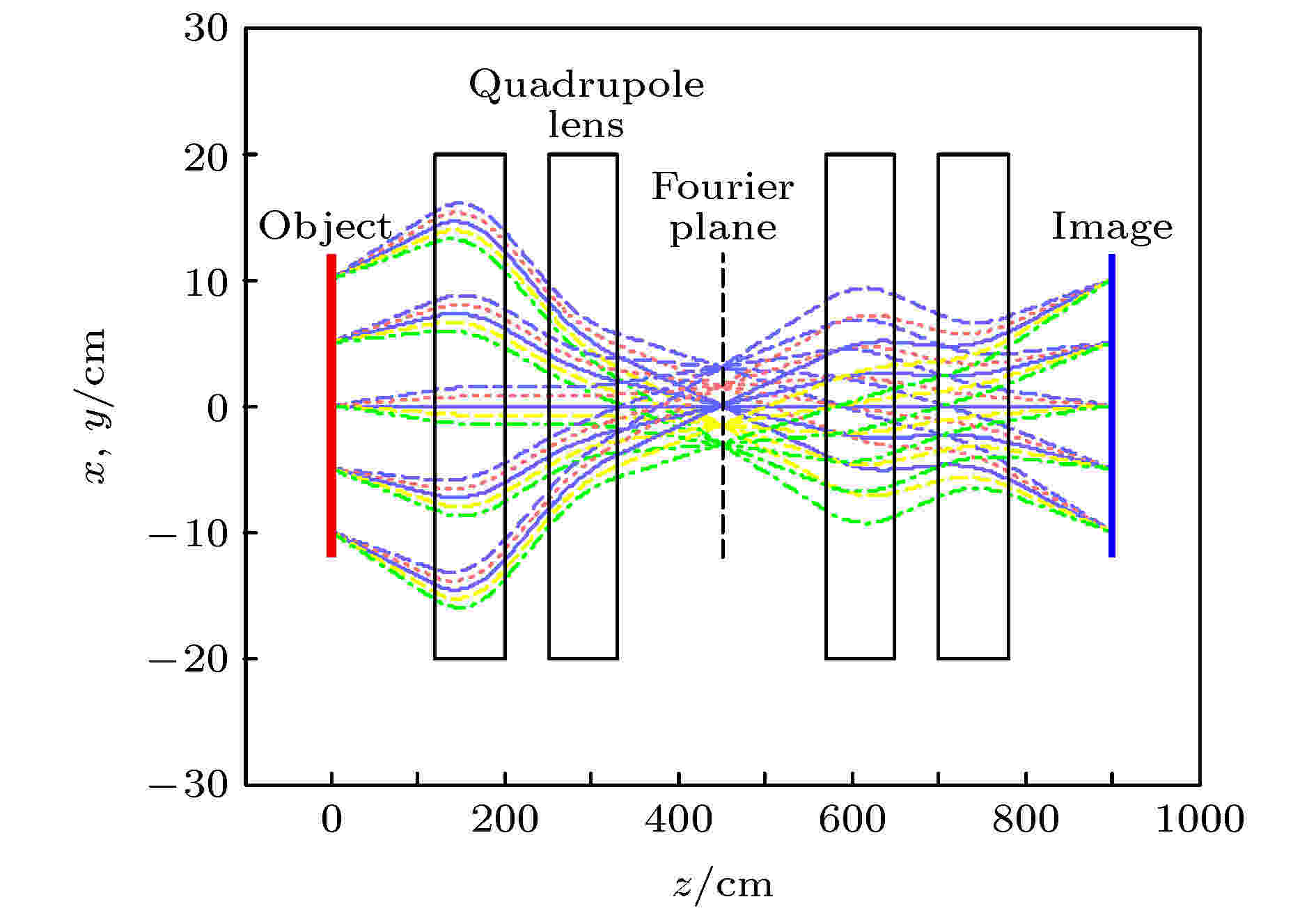
The proton imaging system is composed of four quadrupole magnetic lenses and a collimator. The quadrupole magnetic lenses can realize point-to-point imaging, and the collimator can improve image quality by controlling proton flux and realize material diagnosis. The magnetic field gradient of an ideal quadrupole lens becomes zero at the edge. Inside the lens, the magnetic field gradient is constant along the axis, while the magnetic field boundary of the actual lens extends outward. In the proton imaging system, the fringing field will affect the proton transport state and the performance of the imaging system as well. In this paper, a method to optimize the system is presented when the fringe field is considered. A proton imaging system of 1.6 GeV is established with the Geant 4 program, in which the magnetic field gradient distribution of the actual lens is approximated by the Bell function. In an ideal imaging system, the external drift length is 1.2 m, the internal drift length is 0.5 m, the length of the magnet is 0.8 m, and the magnetic field gradient is 8.09 T/m. The parameters of the practical imaging system can be obtained by using the optimization method: when the integral difference in magnetic field gradient distribution between the actual lens and the ideal lens is equal to zero, the outer drift length of the imaging system is 1.203 m and the inner drift length is 0.506 m; when the integral difference in the magnetic field gradient distribution between the actual lens and the ideal lens is equal to 1%, the outer drift length is 1.208 m and the inner drift length is 0.516 m. In the numerical simulation, a 1mm-thick copper plate and a concentric ball are chosen as the objects, and the influence of the fringing field on the collimator aperture and that on the proton flux error are studied. The results show that the optimized imaging system can reduce the flux error of protons passing through the object, and the difference in the aperture of collimator is on the order of 10–2 when the integral difference is on the order of 10–2 in magnitude.
ATOMIC AND MOLECULAR PHYSICS
2021, 70 (2): 023201.
doi: 10.7498/aps.70.20201236
Abstract +
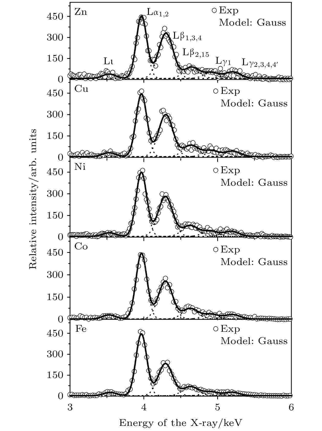
The L-shell X-ray emissions of iodine are investigated as a function of target atomic number for 4.5-MeV I20+ ions impacting on Fe, Co, Ni, Cu and Zn targets. Six distinct L-subshell X-rays are observed. The energy of the x-ray has a blue shift compared with the atomic data. The relative intensity ratio of Lβ1, 3, 4 and Lβ2, 15 to Lα1, 2 almost increase linearly with the target atomic number increasing. The ratio of I(Lι) to I(Lα1, 2) and I (Lγ2, 3, 4, 4') to I(Lγ1) are approximately proportional to the square of target atomic number. It is indicated that during the interaction of highly charged heavy ions with atom in the energy region near the Bohr velocity, the inner-shell process is mainly caused by the close-range collisions below the surface. There, the projectile not only has enough time to capture electrons from the target atom to be neutralized, but also has enough kinetic energy to ionize the inner-shell electron by coulomb interaction. At the balance between electron capture and ionization, the outer-shells of M, N, O etc. could be multiply ionized. The extent of multiple ionization increases with the target atomic number increasing. That leads to the energy shift, resulting in the change of the relative intensity ratio for the L-subshell X-ray. The smaller the atomic fluorescence, the larger the enhanced fluorescence caused by multiple ionization.
ELECTROMAGNETISM, OPTICS, ACOUSTICS, HEAT TRANSFER, CLASSICAL MECHANICS, AND FLUID DYNAMICS
2021, 70 (2): 024201.
doi: 10.7498/aps.70.20200964
Abstract +
2021, 70 (2): 024301.
doi: 10.7498/aps.70.20201375
Abstract +
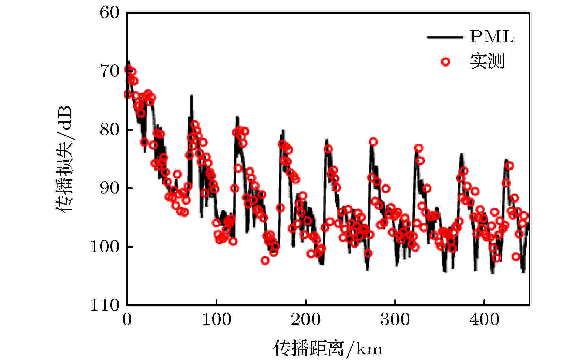
In a deep sea sound channel, rays will bend due to the sound speed profile, and convergence zone will occur when the rays are intensive. Transmission loss in the convergence zone is smaller and it is conducive to acoustic detection and communication. Therefore the study of acoustic characteristics in convergence zone is always the focus of deep-sea acoustics. A long-range sound propagation experiment is conducted in the South China Sea. An equivalent broadband explosive sound source of 1 kg is placed at a depth of 200 m, and the hydrophone receives the data at 3146 m far. The processing and analysis of the experimental data indicate that there is a convergence zone below the sound channel axis in the incomplete deep channel. Compared with the upper turning point convergence zone near the surface, this convergence zone has a high convergence gain at a long distance. The caustic lines of refracted type and refracted surface-refleted type are determined by means of ray-normal mode theory. It is found that the location of the deep convergence zone observed in the experiment is consistent with the position of the refracted caustic line. It is proved that the convergence zone is a lower turning point convergence zone formed by the superposition of a large number of normal modes in the same phase, and it has a convergence effect at a certain depth below the sound channel axis in the deep sea. The formation conditions of the convergence zone and the influence of sound source depth on the caustic structure of the convergence zone are studied. The comparisons of the transmission loss and the width between the upper and lower turning point convergence zone at a long distance aremade. The analysis shows that the convergence gain in the seventh lower turning point convergence zone is still no less than 10 dB. The influence of the vertical structure of sound velocity on the lower turning point convergence zone is studied. The theoretical analysis results are in good agreement with the experimental data.

2021, 70 (2): 024601.
doi: 10.7498/aps.70.20201057
Abstract +
In physics, the non-linear mode coupling is an important strategy to manipulate the mechanical properties of a vibrational system. Compared with the single-mode nonlinear system, the complex systems with two- or multi-mode nonlinear coupling have garnered considerable attention, among which the analytical solutions to the coupled Duffing equations are widely studied to solve nonlinear coupling. The fact is that the solving of the Duffing coupling equations generally starts with the eigenmodes solution of the linear equations. The trial solution of the coupled equations is the linear superposition of the eigenmodes. Under the secular perturbation theory and similar conditions, the Duffing coupling equation degenerates into two decoupled equations. However, thus far most of the solution methodologies are too complicated to unravel the underlying physical essence clearly. In this paper, first, by applying the representational transformation to the linear terms of the first-order coupled Duffing equations and the secular perturbation theory for the nonlinear terms, a decoupled expression of the first-order Duffing equations is derived, which can be solved more straightforwardly. Subsequently, in order to verify the correctness of the method, we design a coupled tuning fork mechanical vibration system, which consists of two experimental instruments to provide driving force and receive signals, two tuning forks and springs. The amplitude spectra are measured by an experimental instrument of forced vibration and resonance (HZDH4615), which provides a periodic driving signal for the tuning fork. The numerical fitting by software is employed to clarify the mechanism of the spectrum. Theoretically, the obtained fitting parameters can also evaluate some important attributes of the system. Most strikingly, due to the nonlinear coupling the splitting of the resonant peak and the phenomenon of “hysteresis loop” are clearly observed in the experiment. The research shows that the experimental results perfectly match the theoretical results obtained before. The method of solving coupled nonlinear equations in this article provides a solution and improvement of flexible adoption of nonlinear theory. On the other hand, it can be extended to coupled light and electricity systems, offer certain guidance for understanding the dynamic behavior of coupled systems, and will be conductive to the quantitative examination of numerous nonlinear coupling devices.
2021, 70 (2): 024701.
doi: 10.7498/aps.70.20201048
Abstract +
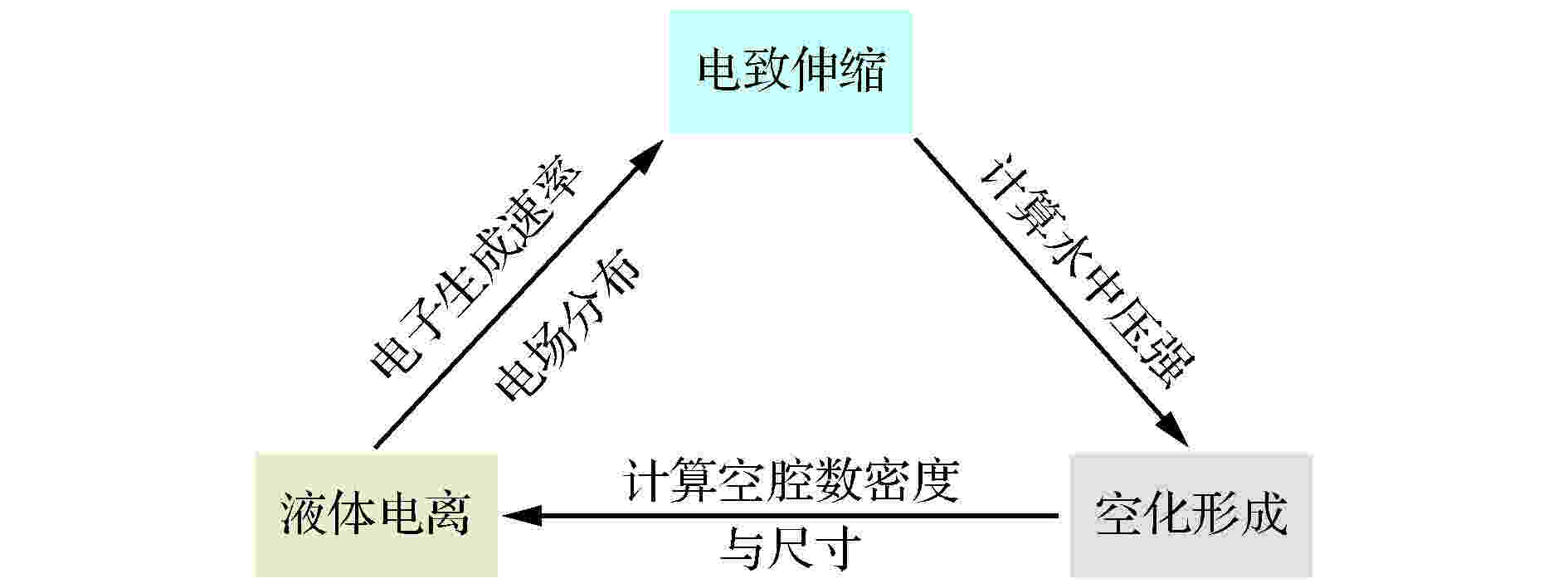
Underwater nanosecond-pulsed discharges have been widely utilized in numerous industrial applications. The initial stage of nanosecond-pulsed discharge in water contains extremely abundant physical processes, however, it is still difficult to reveal the details of charge transportation and multiplicative process in liquid within several nanoseconds by currently existing experimental diagnostic techniques. Up to now, the initiation mechanism of underwater nanosecond discharge has been still a puzzle. In this paper, we develop a two-dimensional axially symmetric underwater discharge model of pin-to-plane, and numerically investigate the electrostriction process, cavitation process, and ionization process in water, induced by nanosecond-pulsed voltage. The negative pressure in water caused by tensile ponderomotive force is calculated. The creation of nanoscale cavities (so-called nanopores) in liquid due to negative pressure is modeled by classical nucleation theory with modified nucleation energy barrier. When estimating the temporal development of nanopore radius, a varying hydrostatic pressure is considered to restrain the unlimited expansion of nanopores. We estimate the electron generation rate by the product of the generation rate of incident electrons and the number density of nanopores. The simulation results show that cavitation occurs in liquid within several microns from pin electrode due to the electrostriction, which results in the formation of a large number of nanopores. The expansion of nanopore, caused by electrostrictive pressure on nanopore surface, provides a sufficient acceleration distance for electrons. The impact ionization of water molecules can be triggered by energetic electrons, leading the local liquid to be ionized rapidly. The effects of nanopores on rapid electron generation in water are discussed. Once nanopores are formed, the electrons can be generated in the following ways: 1) Field ionization of water molecules on the nanopore wall continuously provides seed electrons; 2) the seed electrons accelerated in nanopores enter into the liquid and collide with water molecules, resulting in the rapid increase of electrons. It can be inferred that the randomly scattered nanopores act as micro-sources of charges that contribute to the continuing ionization of liquid water in cavitation region near pin electrode. Electrostriction mechanism provides a new perspective for understanding the initiation of nanosecond-pulsed discharge in water.

2021, 70 (2): 024702.
doi: 10.7498/aps.70.20201192
Abstract +
With the rapid development of micro-nano technology and aerospace technology, researches related to rarefied gas flows have received more and more attention. For micro-/nanoscale systems and spacecraft in a rarefied environment, the reduction in the frequency of intermolecular collisions in the flow field makes the interaction between gas molecules and the solid surface develop into a major factor affecting the flow state. However, the mechanism of gas-surface interaction in rarefied flow has not been fully revealed due to its microscopic nature and physical complexity, and the existing simulation methods cannot accurately reflect the effect of this process on the flow state. In this paper, molecular beam method is adopted to simulate the scattering process of argon molecules on platinum surface, and the impacts of incident velocity, angle and wall roughness on the momentum and energy conversion mechanism are explored. By simulating the molecular scattering process under the two incident angles of $ 5^{\circ} $ and $ 75^{\circ}$ , the following conclusions are obtained. When colliding with the wall at an angle close to vertical, both components of the momentum of the gas molecules are lost. The normal energy transfers to the tangential direction, and when the molecular velocity is not less than 2.0, the transfer rate is not significantly affected by the incident energy of the molecule and the surface roughness. The total energy loss of gas molecules after scattering becomes significant with the increase of incident velocity, and it is not sensitive to changes of surface roughness. When the gas molecules are incident at $ 75^{\circ} $ , the roughness of the surface has a significant impact on the conversion mechanism of molecular momentum and energy. After colliding with a smooth wall, the momentum and energy values of the gas molecules remain basically unchanged, only the direction of the momentum is reversed. The motion state of molecules is close to the mirror reflection, and the conversion between momentum and energy components is not obvious. The introduction of roughness enhances the degree of accommodation between gas molecules and metal surface, and promotes the transfer of molecular tangential momentum and kinetic energy to the normal direction. When incident at a large polar angle, as opposed to the small-angle cases, the total energy loss of molecules is not sensitive to changes of incident velocity, it goes up significantly with the surface roughness increasing. The research in this article not only explores the gas-surface interaction mechanism, but also provides a useful reference for the high-fidelity simulation of rare gas flow and the development of appropriate gas-surface interaction models.
CONDENSED MATTER: ELECTRONIC STRUCTURE, ELECTRICAL, MAGNETIC, AND OPTICAL PROPERTIES
2021, 70 (2): 027101.
doi: 10.7498/aps.70.20200885
Abstract +
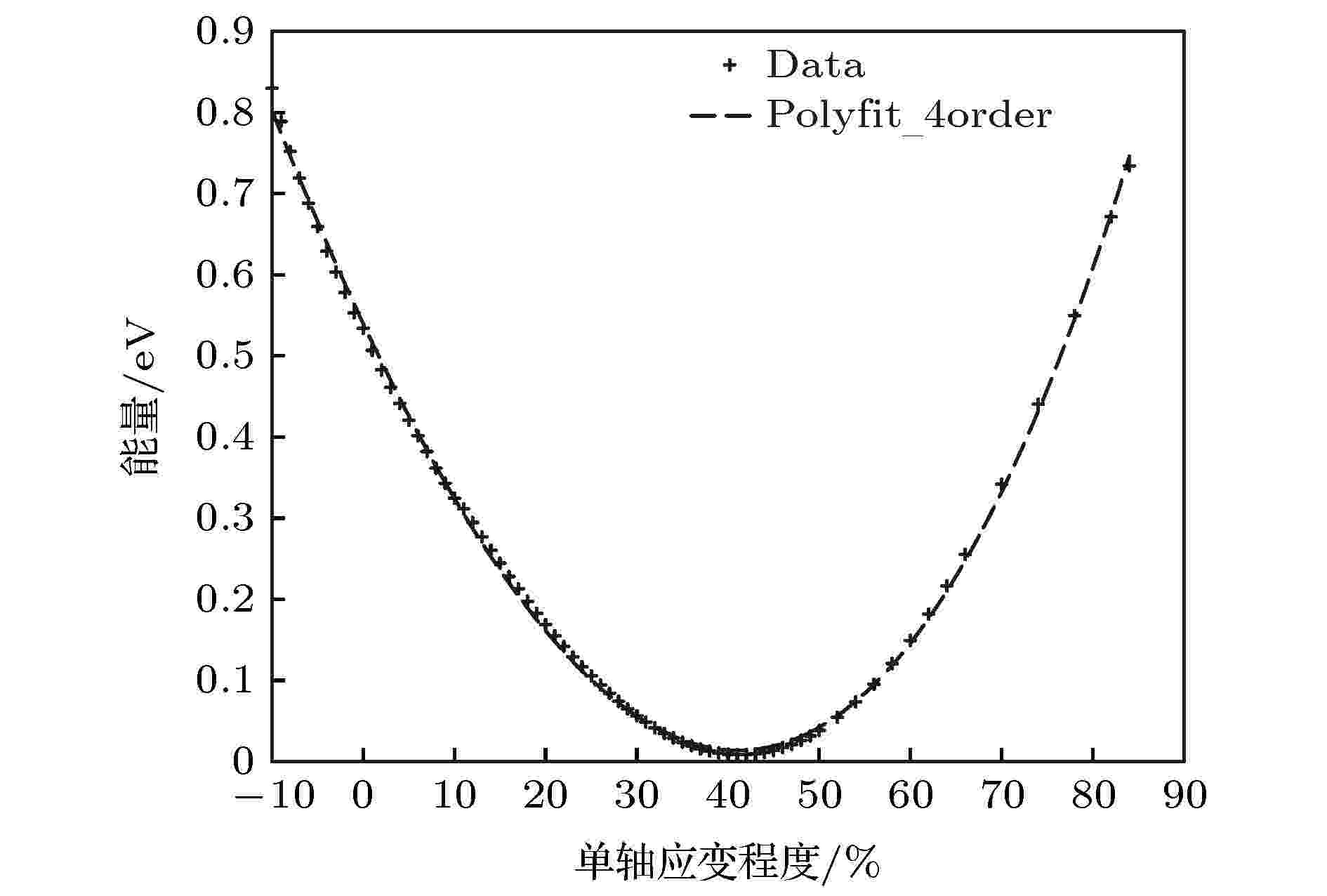
Half-Heusler semiconductors exhibit similar properties: the differences among their properties lie only in the fact that in ternary compositions the zinc-blende binary substructure does not provide the required 18 electrons, but this is improved by adding an extra transition metal, which restores the electronic balance. Half-Heusler ternary compound with 18 valence electrons under an appropriate uniaxial strain is a topological insulating phase. Most importantly, it is proposed that in the half-Heusler family, the topological insulator should allow the incorporating of superconductivity and magnetism. Using the first-principle full-potential linearized augmented wave method we study the band structure of a series of Li(Na)AuS topological insulators. The electronic and magnetic properties of Heusler alloys are investigated by the WIEN2k package. The exchange-correlations are treated within the generalized gradient approximation of PerdeweBurke and Ernzerhof (GGA), the local spin density approximation (LSDA), by using the modified Becke-Johnson exchange potential and the correlation potential of the local-density approximation (MBJ). Spin-orbit coupling is treated by means of the second variational procedure with the scalar-relativistic calculation as basis. We first determine the equilibrium lattice constants by calculating the total energy. The theoretical lattice constant of LiAuS full-potential GGA is 6.02 Å, which is somewhat greater than the result of pseudopotential(5.99 Å). The calculated equilibrium lattice parameter is 5.86 Å for LSDA. Most of the half-Heusler compounds have band inversion, and open the nature band gaps, but the gap of MBJ is not very good. Smaller uniaxial stress damages the cubic structure and also such a natural band gap of topological insulators. By applying uniaxial tensile stress until the equilibrium position is reached in all directions of the structure, the system band gap value is about 0.2 eV, which is consistent with the result obtained from the band gap of cubic structure equilibrium position. When uniaxial tensile stress is 41%, the system turns into a tetragonal structure, the equilibrium lattice constant is a = 5.2477 Å and c/a = 1.41. We use the method of substitution of homologous elements to ensure the properties of topological insulator of materials without changing the cubic structure, and open the bandgap of materials under the equilibrium lattice constant of the system, thereby improving the feasibility of experimental synthesis of topological insulator materials. Our results for the doping suggest that epitaxial strain encountered during experiment can result in electronic topological transition. We hope that the results presented here conduce to further experimental investigation of the electronic topological transition in half-Heusler compounds.
2021, 70 (2): 027103.
doi: 10.7498/aps.70.20200845
Abstract +
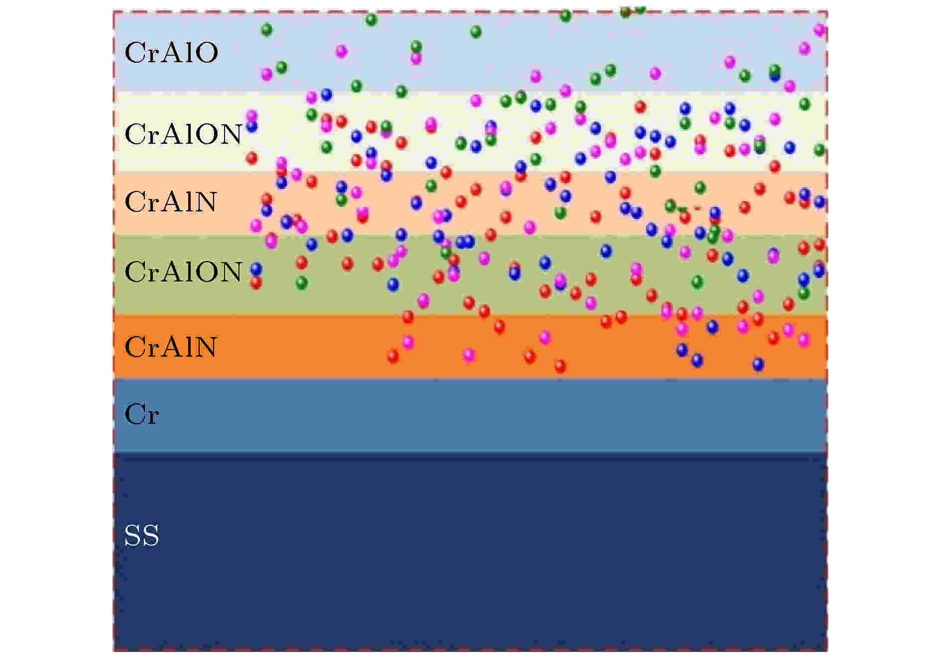
Spectrally selective absorbing coating is the core component of the utilization of solar energy. The spectral properties of selectively absorbing coating directly determine the conversion efficiency of constructing solar power plants. To enhance the selective absorbability and thermal stability, we propose an idea that these metal particles are replaced with transition-metal nitrides, and then coated with periodic nanocrystalline-amorphous heterogeneous structures. Double-absorbing layer Cr/CrAlN/CrAlON/CrAlN/CrAlON/CrAlO solar selective absorbing coatings with a high solar absorptance of 0.90 and a relatively low emittance of 0.15 are obtained by the cathodic arc ion plating technique. After the coating is aged at 500 °C in air for 220 h, its absorptance increases to 0.94 and the emittance decreases to 0.10. More importantly, the coating exhibits an outstanding thermal stability with a selectivity of 0.94/0.11 even after being aged at 500 °C for 1000 h in air. The microstructure analysis indicates that the multilayer coating consists of aperiodic CrAlN and CrAlON layers in addition to the Cr and CrAlO layers. Through the long-term aging, a small number of AlN, CrN and Cr2N nanocrystallites are observed to be homogeneously embedded in the CrAlN and CrAlON amorphous matrices. The nanoparticles in the CrAlN and CrAlON layers can effectively scatter the incident light into a broadband wavelength range, increasing the optical path length in the absorbing layers, and thus resulting in a pronounced enhancement in the absorptivity. A handful of Cr2O3 and Al2O3 nanograins are observed to be embedded in the amorphous CrAlO antireflection layer, which can effectively reflect the solar infrared radiation and the thermal emittance from the substrate, and thus resulting in pretty low infrared emissivity. The good thermal stability is attributed to the excellent thermal stability of the dielectric amorphous matrices and the sluggish atomic diffusion in the nanoparticles, which could effectively slow down the inward diffusion of oxygen and avoid agglomerating the nanoparticles. These results are of great importance for enhancing the overall performance of cermet spectrally selective absorption coating and also for improving the conversion efficiency of solar energy photo-thermal utilization.

2021, 70 (2): 027803.
doi: 10.7498/aps.70.20201150
Abstract +
2021, 70 (2): 027804.
doi: 10.7498/aps.70.20201173
Abstract +
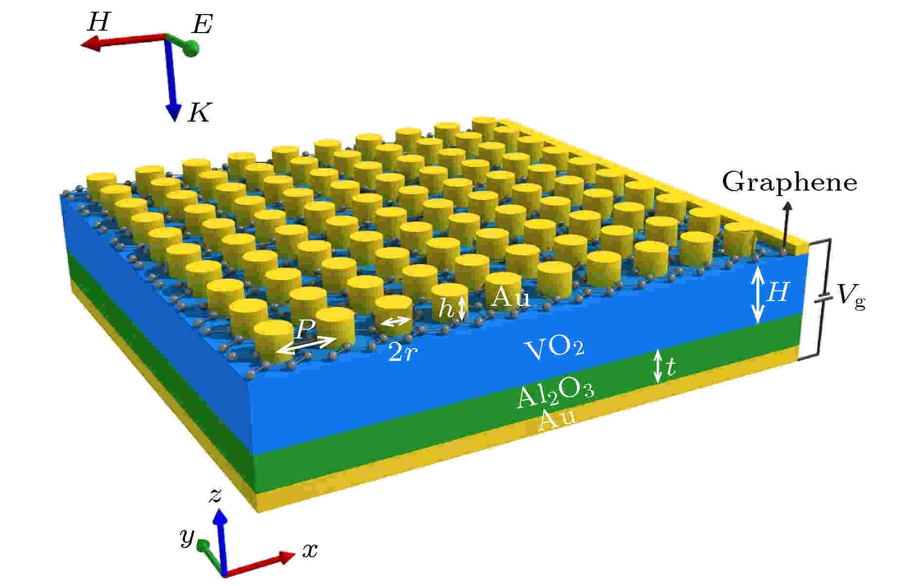
The metamaterial perfect absorber (MPA) is a new type of electromagnetic wave absorber first proposed by Landy. Compared with the traditional electromagnetic wave absorber, MPA has many advantages, including ultra-high absorption efficiency, ultra-thin, compact structure, easily tunable resonances, etc. so it is gradually applied to ultra-sensitive sensing, imaging, detection and other fields. Nowadays, the MPA research focuses on two areas. One area focuses on the absorption efficiency modulation and absorption wavelength tuning, and the other area is to broaden the absorption bandwidth and achieve high absorptions at different optical frequencies. Previously, the MPA absorption efficiency modulation or absorption wavelength tuning was realized by changing the device structure or the surrounding medium material. But these methods can increase the difficulty in processing and increase the device volume. In order to achieve the control of absorption wavelength and absorption efficiency without increasing the difficulty in processing or the device volume. We propose to use vanadium dioxide and graphene as the materials of MPA, which has high absorption efficiency in the infrared band. It is found that the absorption efficiency of MPA at 9.66 μm wavelength can reach 96% when the temperature of vanadium dioxide is 5 ℃ by using finite difference time domain (FDTD) method. However, when the vanadium dioxide temperature rises to 68 ℃, the absorption efficiency of MPA suddenly drops to 2.8%. The modulation depth of absorption efficiency can reach 97.08%. We propose that the MPA be able to control not only the absorption efficiency, but also the absorption wavelength. By changing the voltage of graphene, the chemical potential Ef of graphene can be controlled and the absorption wavelength of MPA can be tuned. When Ef increases from 0.1 eV to 3 eV, the absorption wavelength of MPA will be blue-shifted from 9.66 μm to 6.46 μm. The magnetic field distribution of MPA at the absorption wavelength shows that the MPA has a high absorption efficiency because of the Fabry-Pérot (FP) cavity resonance is formed in MPA. Therefore, the change of structure parameters of MPA will affect its absorption characteristics. It is found by the FDTD method that the absorption wavelength of MPA will be redshifted, when the radius, thickness, period and thickness of the nanocolumn array increase. This study can provide theoretical guidance for designing and preparing the controllable MPA, which has compact structure and low process difficulty merits.
INTERDISCIPLINARY PHYSICS AND RELATED AREAS OF SCIENCE AND TECHNOLOGY
2021, 70 (2): 028401.
doi: 10.7498/aps.70.20200954
Abstract +
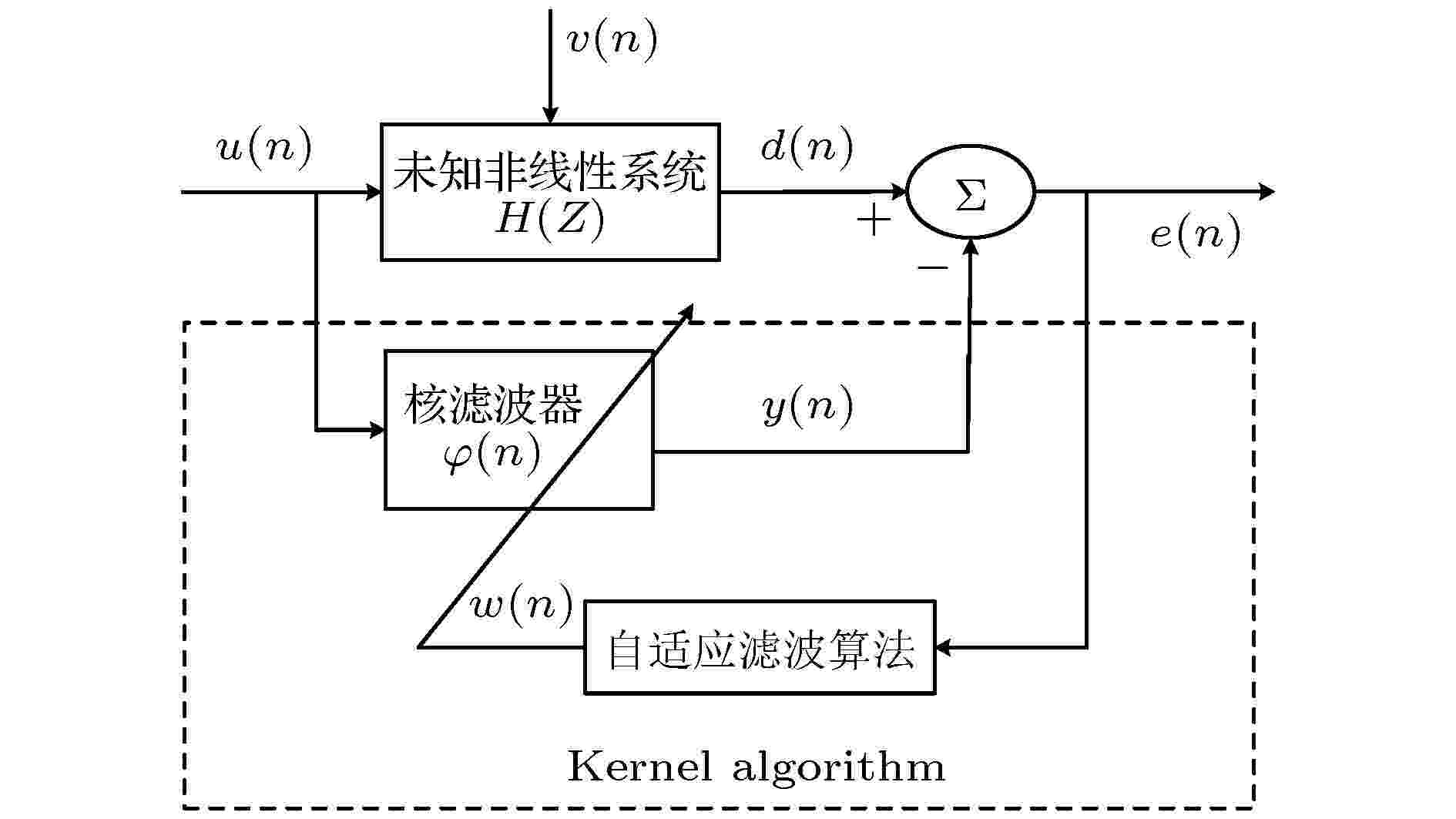
Kernel adaptive filters are a class of powerful nonlinear filter developed in reproducing kernel Hilbert space (RKHS).The Gaussian kernel is usually the default kernel in KAF algorithm, because the Gaussian kernel has the universal approximation. However, in previous research the kernel adaptive filtering algorithms were mostly based on mean square error criterion and assumed to be in a Gaussian noise environment. When environmental noise is changed, the performance of conventional kernel adaptive filtering algorithm based on mean square error criterion is seriously reduced to failure due to the interference of non-Gaussian noise and the influence of inappropriate non-Gaussian modeling. Therefore, it is important to develop a new method of suppressing the noise of non-Gaussian signals. In this paper, a new kernel fractional lower power adaptive filtering algorithm is proposed by combining the benefits of the kernel method and a new loss function which is robust against non-Gaussian impulsive interferences and has fast convergence under a similar stability condition. The proposed SP-KFLP algorithm generates a new framework of cost function which combines the Softplus function with the KFLP algorithm by updating its weight vector according to the gradient estimation while nonlinear saturation characteristics of output error are used. Compared with the features of sigmoid function the features of the Softplus function guarantee the SP-KFLP an excellent performance for combatting impulsive interference and speeding up the convergence rate. In the kernel fractional low power criterion the reciprocal of the system error is used as the coefficient of the weight vector update formula, and the method of error burst is used to make the weight vector not update to resist the impulse noise. The mean square convergence analysis for SP-KFLP is conducted, and a sufficient condition for guaranteeing convergence is therefore obtained by using the energy conservation relation. The proposed algorithm is very simple computationally. Simulations in a system identification show that the proposed SP-KFLP algorithm outperforms the kernel least-mean-square algorithm, kernel fractional lower power algorithm, and sigmoid kernel fractional lower algorithm in terms of convergence rate and the robustness of against impulsive interference. The proposed algorithm improves not only the capability of resisting impulsive interference, but also the convergence rate. In other words, the contradiction between convergence and tracking performance stability is well taken into account, and the performance under Gaussian noise is also better than the performance of the traditional kernel adaptive algorithm.

2021, 70 (2): 028501.
doi: 10.7498/aps.70.20200741
Abstract +
Two-dimensional (2D) hexagonal boron nitride (hBN) possesses many unique properties such as high mechanical strength and excellent chemical and thermal stability. The 2D hBN exhibits a wide bandgap in the UV region and optically-stable ultra-bright quantum emitters that make hBN a promising nanophotonic platform for quantum computing and information processing, especially in the visible wavelength range. Therefore, it is greatly important to build up different nanophotonic devices with different functionalities based on this material platform to achieve the integrated photonic chips. Among the devices, the integratable optical asymmetric transmission devices are important elements for functional quantum computing chips. Since hBN is a dielectric material, photonic crystal (PhC) structure is the most suitable in principle and allows on-chip integration with other photonic devices. In this study, we theoretically design an asymmetric transmission device based on 2D hBN PhC heterostructures in the visible wavelength range for the first time. Due to the relatively low refractive index of 2D hBN material (n < 2.4), we design a free-standing hBN PhC heterostructure to maximize the light trapping in the structure and minimize the propagation loss. The asymmetric transmission device is composed of two square-lattice 2D PhC structures, namely PhC 1 and PhC 2. We use the plane wave expansion method (PWM) to calculate the iso-frequency contours (EFCs) of the PhC structures to study the light propagation inside of the PhCs, which will propagate along the gradient of direction of the EFCs. We design the PhC structure in the way that the incident light beams from different angles can be self-collimated along the Г-X direction of the PhC 2 and coupled out. On the other hand, the backward incident light is blocked by the bandgaps of PhC 2. In this way, asymmetric optical transmission is achieved with high forward transmittance and contrast ratio. In addition, we further finely tune the structural parameters, including the lattice constant and column radius of the PhCs to optimize the performance by using the finite difference time domain (FDTD) method. The resulting 2D hBN PhC heterostructure achieves an asymmetric transmission in a wavelength range of 610–684 nm with a peak forward transmittance of 0.65 at a wavelength of 652 nm. Meanwhile, the backward transmittance is controlled to be 0.04. As a result, the contrast ratio can reach up to 0.95. The working bandwidth of the hBN PhC is 74 nm (TF > 0.5). In addition, the designed asymmetric transmission device has a small size of 11 μm × 11 μm, thus it is suitable for on-chip integration. Our results open up possibilities for designing new nanophotonic devices based on 2D hBN material for quantum computing and information processing. The design principle can be generally used to design other photonic devices based on 2D hBN material.
2021, 70 (2): 028701.
doi: 10.7498/aps.70.20201170
Abstract +
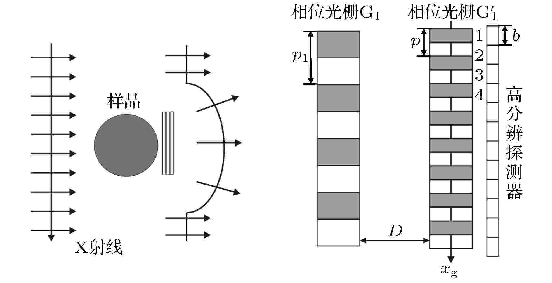
X-ray differential phase contrast imaging technology can reveal the weakly absorbing fine structure which cannot be observed by the conventional X-ray absorption contrast imaging. Hence, it has potential applications in many fields such as medical science, and material science. But in the traditional X-ray grating differential phase contrast imaging system, the analyser grating is used as a spatial filter, and needs to be phase stepped, then multiple exposures are required for information extraction. Thus this leads to high-dose radiation exposure and low efficiency of X-ray utilization. All these disadvantages limit its application in various disciplines. In order to cope with the above issues, a new algorithm based on single-shot grating differential phase contrast imaging system without analyzer grating is proposed. In such a system the absorption, refraction and scattering information can be obtained from one projective image of the sample acquired by a high-resolution detector. The reliability of this new algorithm is confirmed by numerical simulation. Compared with the phase stepping algorithm, the proposed algorithm can provide very accurate and reliable information extraction results without requiring the grating period to match with detector pixel size. It facilitates the reduction of the radiation damage to sample. We emphasize that this method is highly compatible with the future X-ray phase contrast imaging clinical applications.


