-
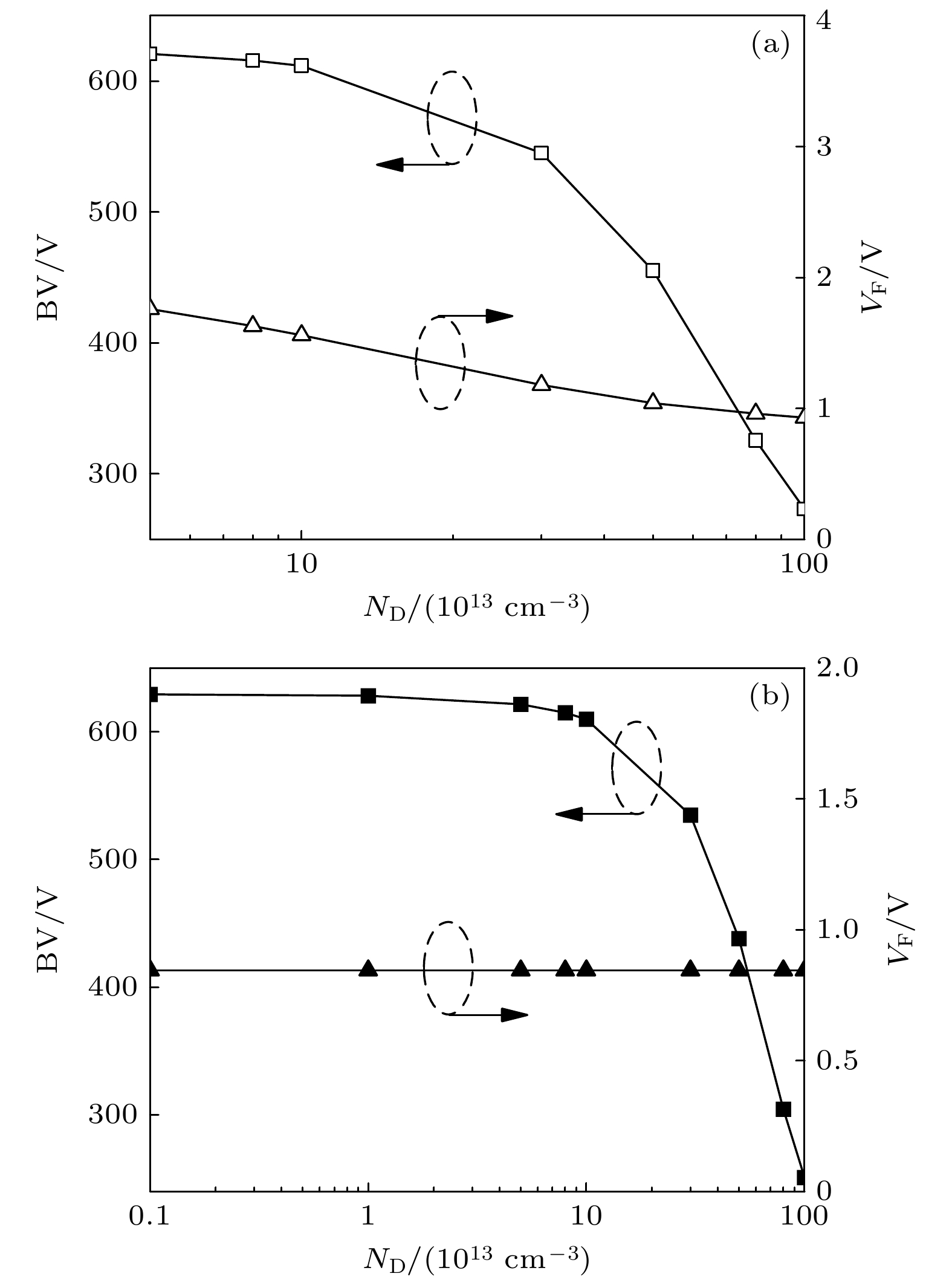
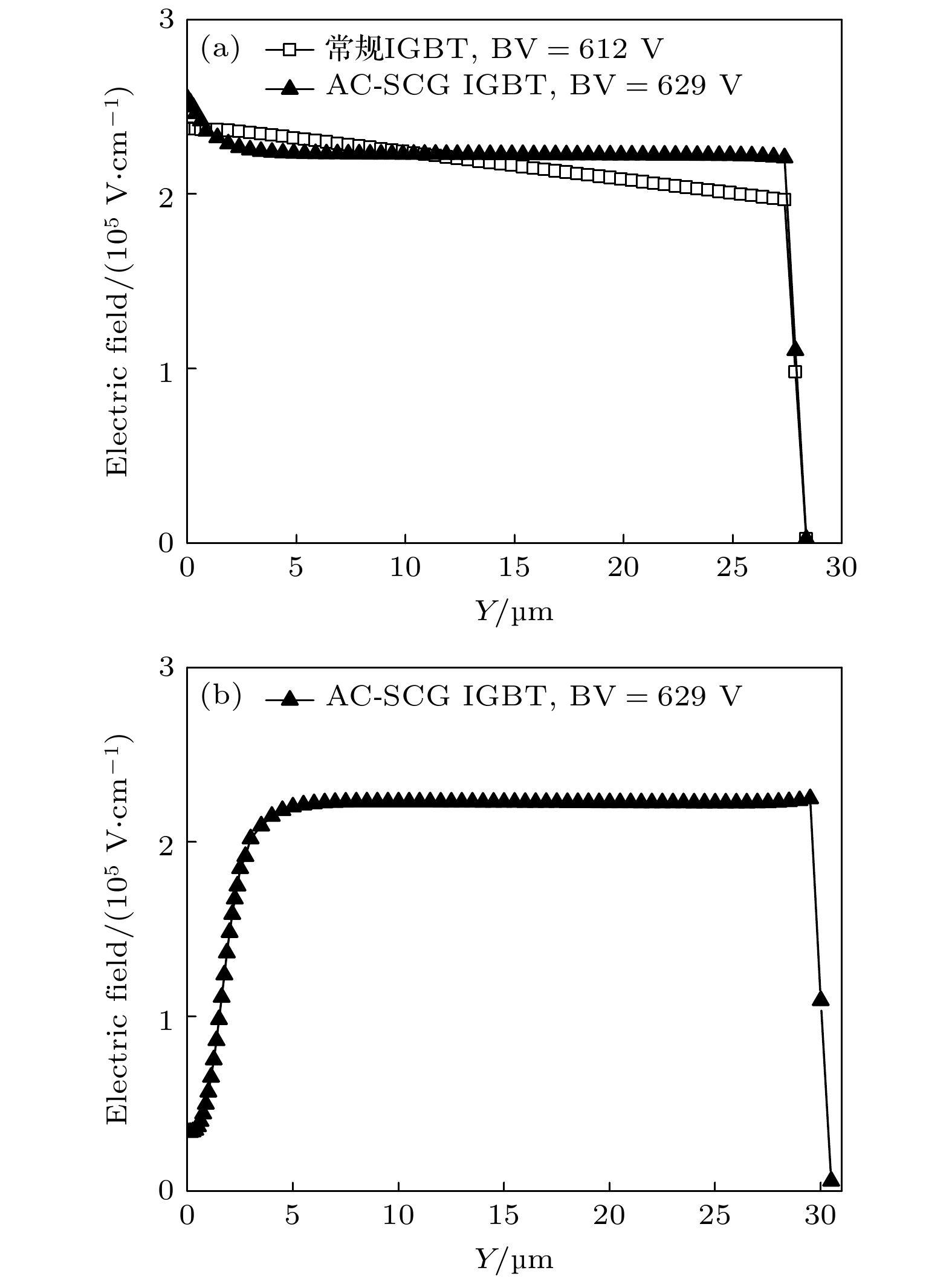
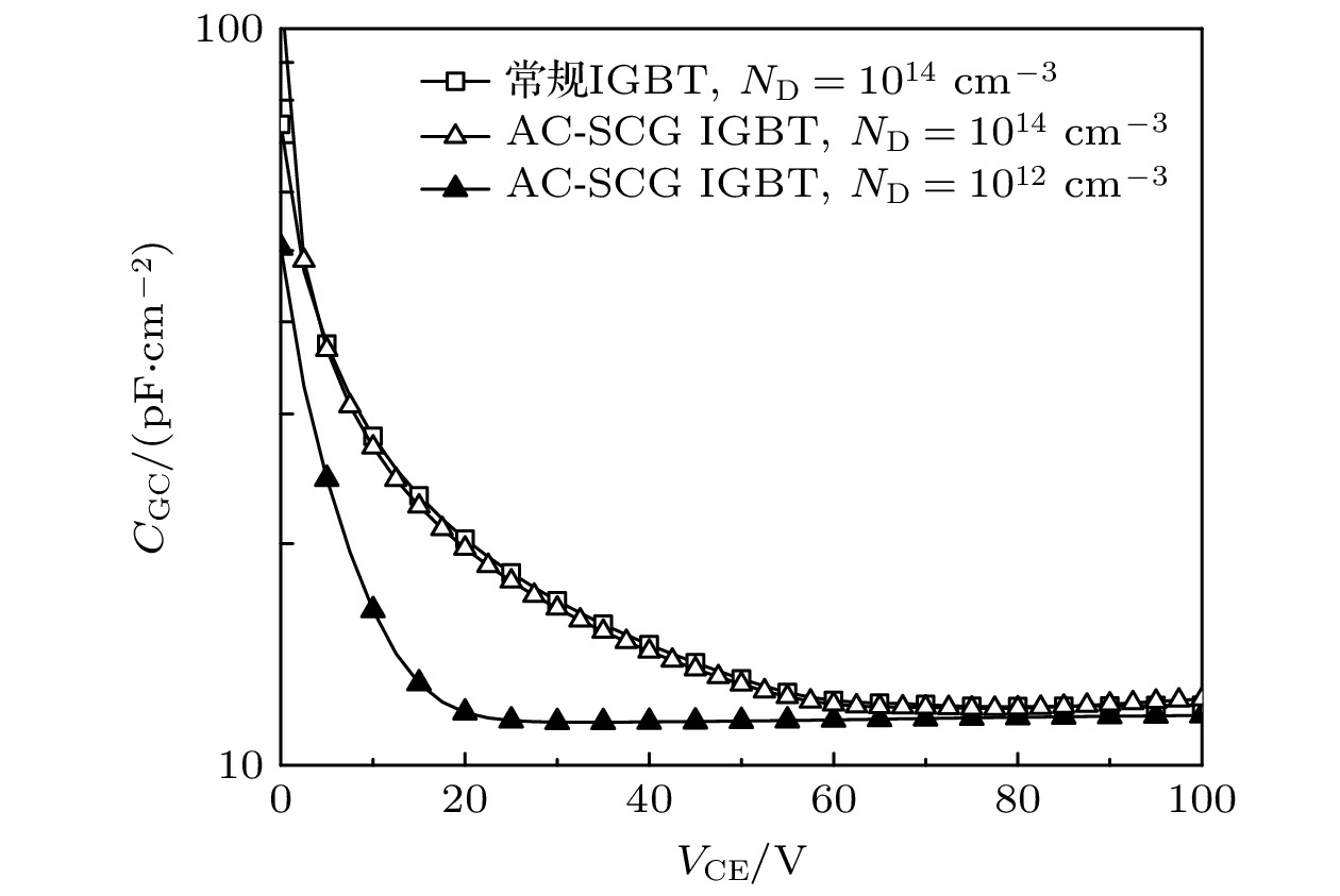
Insulated gate bipolar transistor (IGBT) is the core of modern power semiconductor device, and has been widely used due to its excellent electrical characteristics. A novel majority carrier accumulation mode IGBT with Schottky junction contact gate semiconductor layer (AC-SCG IGBT) is proposed and investigated by TCAD simulation in this article. When the AC-SCG IGBT is in the on-state, a forward bias is applied to the gate. Due to the very low forward voltage drop (VF) of the Schottky barrier diode, the potential of the gate semiconductor layer is almost equal to the gate potential, which can accumulate a large number of majority carrier electrons in the drift region. In addition to the electrons existing, these accumulated electrons increase the conductivity of the drift region, thus significantly reducing VF. Therefore, the doping concentration of the drift region is not limited by VF. The lightly doped drift region can make AC-SCG IGBT have a higher breakdown voltage (BV). Moreover, it also reduces the barrier capacitance in the turn-off process, thus the overall Miller capacitance is small, which can quickly turn off and reduce the turn-off time (Toff) and turn-off loss (Eoff). The simulation results indicate that at the BV of 600 V, the VF of 0.84 V for the proposed AC-SCG IGBT is reduced by 46.2% compared with that for the conventional IGBT (VF of 1.56 V). The Eoff of the AC-SCG IGBT (0.77 mJ/cm2) is reduced by 52.5% compared with that for the conventional IGBT (1.62 mJ/cm2), and the Toff (155.8–222.7 ns) is reduced by 30%. The contradiction between VF and Eoff is eliminated. In addition, the proposed AC-SCG IGBT has a better anti-latch-up capability and is coupled with its higher BV, so it has a larger forward biased safe operating area (FBSOA). The proposed novel structure meets the development requirements for future IGBT device performance, and has great significance for guiding the development of the power semiconductor device field.
-
Keywords:
- insulated gate bipolar transistor /
- accumulation mode /
- forward voltage drop /
- turn-off loss
[1] Baliga B J 1979 Electron. Lett. 15 645
 Google Scholar
[2] Baliga B J 1988 IEEE Proc. 76 409
 Google Scholar
[3] 王彩琳 2015 电力半导体新器件及其制造技术 (北京: 机械工业出版社) 第5—7页
Wang C L 2015 New Power Semiconductor Devices and Their Manufacturing Technologies (Beijing: China Machine Press) pp5–7
[4] Baliga B J (translated by Han Z S, Lu J, Song L M) 2013 Fundamentals of Power Semiconductor Devices (Beijing: Publishing House of Electronics Industry) pp399–401 (in Chinses) [巴利加BJ著 (韩郑生, 陆江, 宋李梅译) 2013 功率半导体器件基础 (北京: 电子工业出版社) 第399—401页]
Baliga B J (translated by Han Z S, Lu J, Song L M) 2013 Fundamentals of Power Semiconductor Devices (Beijing: Publishing House of Electronics Industry) pp399–401 (in Chinses) [5] Chang H R, Baliga B J, Kretchmer J W, Piacente P A 1987 International Electron Devices Meeting ( IEDM) Washington, USA, December 6–9, 1987 p674
[6] Takahashi H, Yamamoto A, Aono S, Minato T 2004 16th International Symposium on Power Semiconductor Devices and ICs ( ISPSD) Kitakyushu, Japan, May 24–27, 2004 p133
[7] Takahashi H, Haruguchi E, Hagino H, Yamada T 1996 8th International Symposium on Power Semiconductor Devices and ICs ( ISPSD) Maui, USA, May 23, 1996 p349
[8] Antoniou M, Udrea F, Bauer F, Mihaila A, Nistor I 2012 24th International Symposium on Power Semiconductor Devices and ICs ( ISPSD) Bruges, Belgium, June 3–7, 2012 p21
[9] Li P, Lü X J, Cheng J J, Chen X B 2016 IEEE Electron. Device Lett. 37 1470
 Google Scholar
[10] Vaidya M, Naugarhiya A, Verma S, Mishra G P 2022 IEEE Trans. Electron. Devices 69 1604
 Google Scholar
[11] Xu H, Yang Y F, Tan J J, Zhu H, Sun Q Q, Zhang D W 2022 IEEE Trans. Electron. Devices 69 5450
 Google Scholar
[12] Li L P, Li Z H, Chen P, Rao Q S, Yang Y Z, Wan J L, Wang T Y, Zhao Y S, Ren M 2022 16th International Conference on Solid-State and Integrated Circuit Technology ( ICSICT) Nanjing, China, October 25–28, 2022 p1
[13] Synopsys Sentaurus TCAD Device User Guide 2017
[14] Duan B X, Xing L T, Wang Y D, Yang Y T 2022 IEEE Trans. Electron. Devices 69 658
 Google Scholar
[15] Udrea F, Deboy G, Fujihira T 2017 IEEE Trans. Electron. Devices 64 713
 Google Scholar
[16] Iwamoto S, Takahashi K, Kuribayashi H, Wakimoto S, Mochizuki K, Nakazawa H 2005 17th International Symposium on Power Semiconductor Devices and ICs ( ISPSD) Santa Barbara, CA, USA, May 23–26, 2005 p31
[17] Yamauchi S, Shibata T, Nogami S, Yamaoka T, Hattori Y, Yamaguchi H 2006 18th International Symposium on Power Semiconductor Devices and ICs ( ISPSD) Naples, Italy, June 4–8, 2006 p1
[18] Duan B X, Wang Y D, Sun L C, Yang Y T 2020 IEEE Trans. Electron. Devices 67 1085
 Google Scholar
[19] Wang Y D, Duan B X, Song H T, Yang Y T 2020 IEEE Electron. Device Lett. 41 1681
 Google Scholar
[20] Sun L C, Duan B X, Yang Y T 2021 IEEE J. Electron Devi. 9 409
 Google Scholar
-
表 1 常规IGBT和AC-SCG IGBT的关键参数和电学特性值
Table 1. Key parameters and electrical characteristic values of the conventional IGBT and AC-SCG IGBT.
名称 参数 常规IGBT AC-SCG IGBT 漂移区长度 LD/μm 28 28 器件宽度 W/μm 3.1 3.1 氧化层厚度 TOX/μm 0.1 0.1 漂移区掺杂浓度 ND/cm–3 1014 1012 Nside区掺杂浓度 Nside/cm–3 — 1012 击穿电压 BV/V 612 629 正向导通压降 VF/V 1.56 0.84 关断时间 Toff/ns 222.7 155.8 关断损耗 Eoff/(mJ·cm–2) 1.62 0.77 -
[1] Baliga B J 1979 Electron. Lett. 15 645
 Google Scholar
[2] Baliga B J 1988 IEEE Proc. 76 409
 Google Scholar
[3] 王彩琳 2015 电力半导体新器件及其制造技术 (北京: 机械工业出版社) 第5—7页
Wang C L 2015 New Power Semiconductor Devices and Their Manufacturing Technologies (Beijing: China Machine Press) pp5–7
[4] Baliga B J (translated by Han Z S, Lu J, Song L M) 2013 Fundamentals of Power Semiconductor Devices (Beijing: Publishing House of Electronics Industry) pp399–401 (in Chinses) [巴利加BJ著 (韩郑生, 陆江, 宋李梅译) 2013 功率半导体器件基础 (北京: 电子工业出版社) 第399—401页]
Baliga B J (translated by Han Z S, Lu J, Song L M) 2013 Fundamentals of Power Semiconductor Devices (Beijing: Publishing House of Electronics Industry) pp399–401 (in Chinses) [5] Chang H R, Baliga B J, Kretchmer J W, Piacente P A 1987 International Electron Devices Meeting ( IEDM) Washington, USA, December 6–9, 1987 p674
[6] Takahashi H, Yamamoto A, Aono S, Minato T 2004 16th International Symposium on Power Semiconductor Devices and ICs ( ISPSD) Kitakyushu, Japan, May 24–27, 2004 p133
[7] Takahashi H, Haruguchi E, Hagino H, Yamada T 1996 8th International Symposium on Power Semiconductor Devices and ICs ( ISPSD) Maui, USA, May 23, 1996 p349
[8] Antoniou M, Udrea F, Bauer F, Mihaila A, Nistor I 2012 24th International Symposium on Power Semiconductor Devices and ICs ( ISPSD) Bruges, Belgium, June 3–7, 2012 p21
[9] Li P, Lü X J, Cheng J J, Chen X B 2016 IEEE Electron. Device Lett. 37 1470
 Google Scholar
[10] Vaidya M, Naugarhiya A, Verma S, Mishra G P 2022 IEEE Trans. Electron. Devices 69 1604
 Google Scholar
[11] Xu H, Yang Y F, Tan J J, Zhu H, Sun Q Q, Zhang D W 2022 IEEE Trans. Electron. Devices 69 5450
 Google Scholar
[12] Li L P, Li Z H, Chen P, Rao Q S, Yang Y Z, Wan J L, Wang T Y, Zhao Y S, Ren M 2022 16th International Conference on Solid-State and Integrated Circuit Technology ( ICSICT) Nanjing, China, October 25–28, 2022 p1
[13] Synopsys Sentaurus TCAD Device User Guide 2017
[14] Duan B X, Xing L T, Wang Y D, Yang Y T 2022 IEEE Trans. Electron. Devices 69 658
 Google Scholar
[15] Udrea F, Deboy G, Fujihira T 2017 IEEE Trans. Electron. Devices 64 713
 Google Scholar
[16] Iwamoto S, Takahashi K, Kuribayashi H, Wakimoto S, Mochizuki K, Nakazawa H 2005 17th International Symposium on Power Semiconductor Devices and ICs ( ISPSD) Santa Barbara, CA, USA, May 23–26, 2005 p31
[17] Yamauchi S, Shibata T, Nogami S, Yamaoka T, Hattori Y, Yamaguchi H 2006 18th International Symposium on Power Semiconductor Devices and ICs ( ISPSD) Naples, Italy, June 4–8, 2006 p1
[18] Duan B X, Wang Y D, Sun L C, Yang Y T 2020 IEEE Trans. Electron. Devices 67 1085
 Google Scholar
[19] Wang Y D, Duan B X, Song H T, Yang Y T 2020 IEEE Electron. Device Lett. 41 1681
 Google Scholar
[20] Sun L C, Duan B X, Yang Y T 2021 IEEE J. Electron Devi. 9 409
 Google Scholar
Catalog
Metrics
- Abstract views: 3878
- PDF Downloads: 176
- Cited By: 0


 DownLoad:


