-
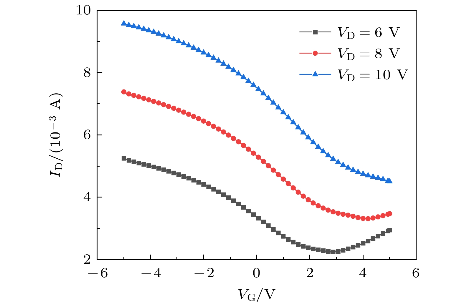
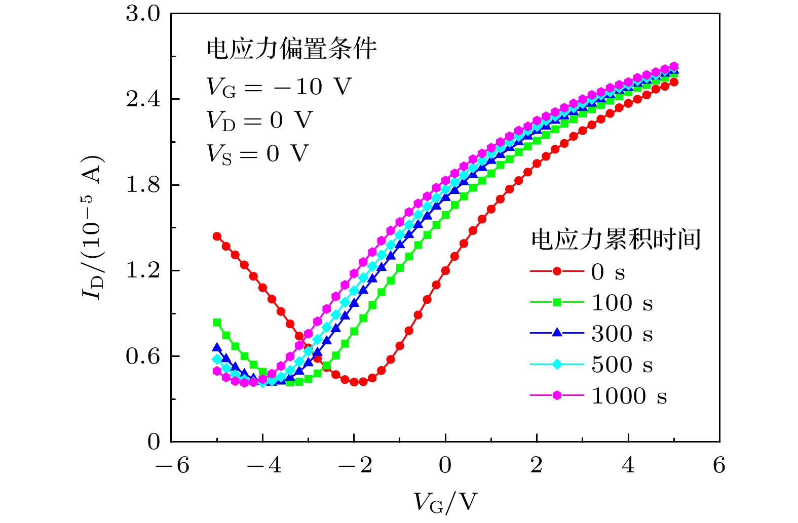
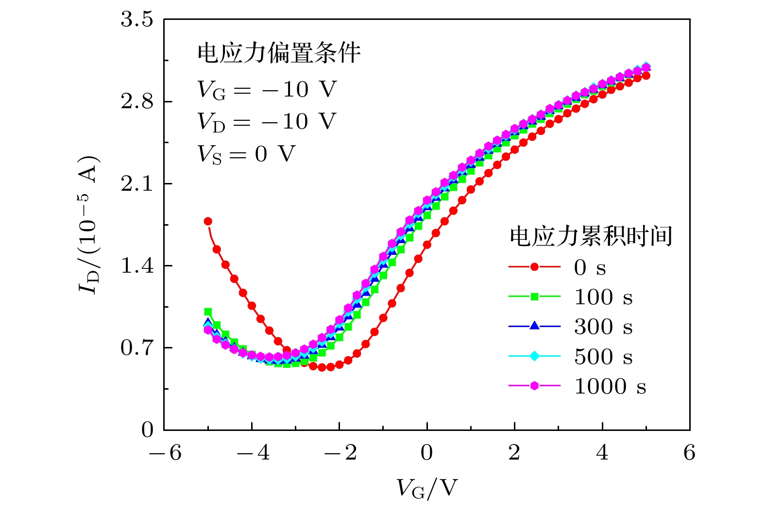
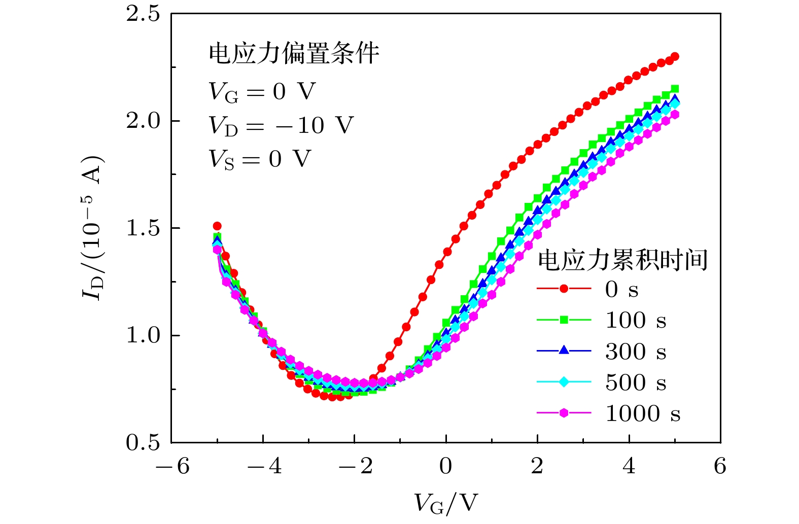
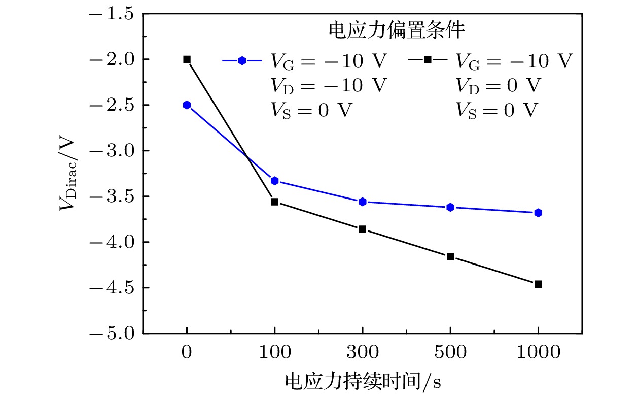
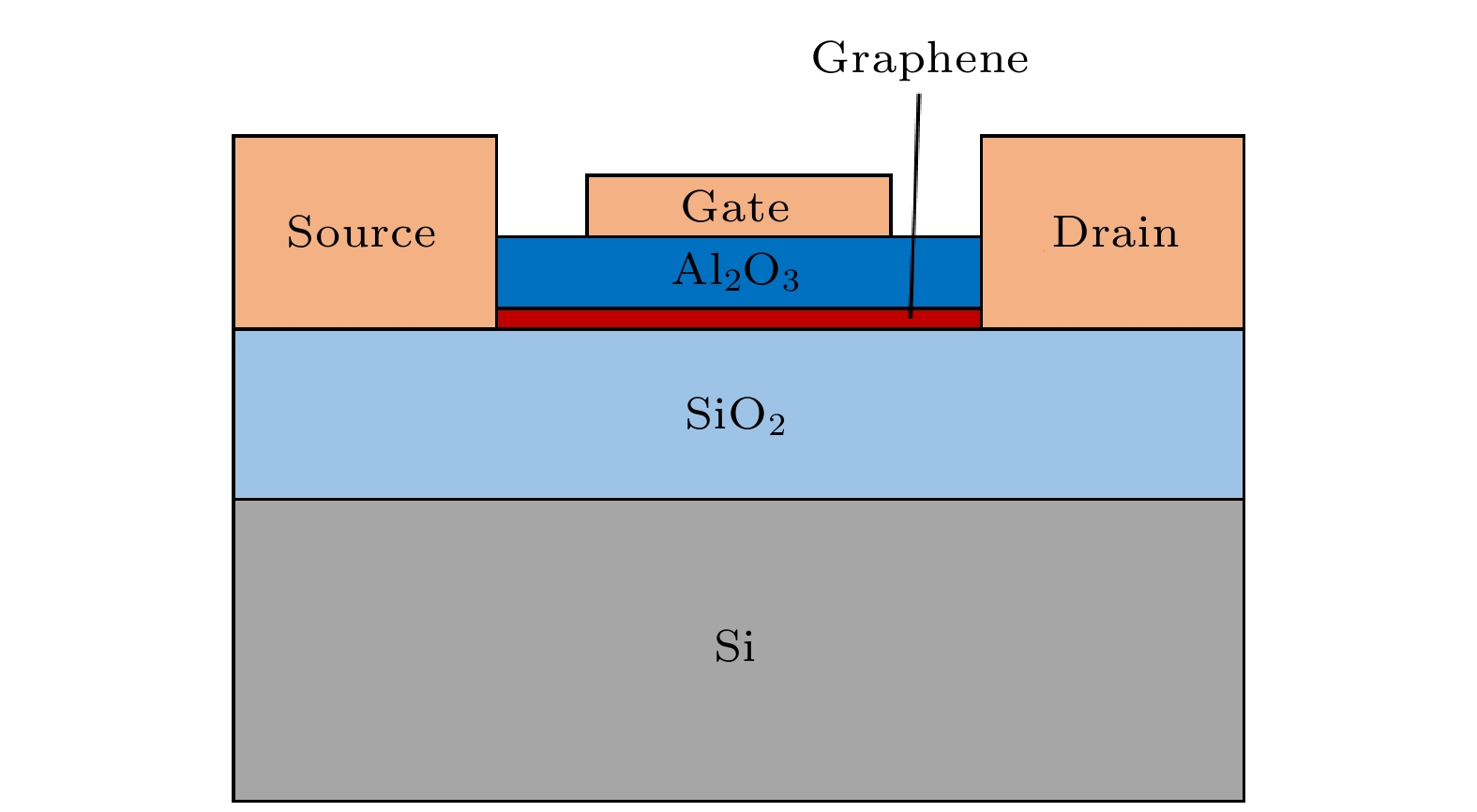
In this paper, graphene field effect transistors (GFETs) with the top-gate structure are taken as the research object. The electrical stress reliabilities are studied under different bias voltage conditions. The electrical pressure conditions are gate electrical stress (VG = –10 V, VD = 0 V, and VS = 0 V), drain electric stress (VD = –10 V, VG = 0 V, and VS = 0 V), and electrical stresses applied simultaneously by gate voltage and drain voltage (VG = –10 V, VD = –10 V, VS = 0 V). Using a semiconductor parameter analyzer, the transfer characteristic curves of GFETs before and after electrical stress are obtained. At the same time, the carrier migration and the Dirac voltage VDirac degradation are extracted from the transfer characteristic curves. The test results show that under different electrical pressures, the carrier mobility of GFETs degrades continuously with the increase of electric stress time. Different electrical pressure conditions have varying effects on the drift direction and degradation of VDirac: gate electrical stress and drain electrical stress cause VDirac drift of the device in opposite directions, and the gate electrical stress is greater than the electrical stress applied by both gate voltage and drain voltage, leading to VDirac degradation of GFETs. An analysis of the causes indicates that different electrical stresses produce different electric field directions in the device, which can affect the carrier concentration and movement direction. Electrons and holes in the channel are induced and tunnel into the oxide layer, and they are captured by trap charges in the oxide layer and at the interface between graphene and oxide, forming oxide trap charges and interface trap charges. This is the main reason for reducing carrier mobility of GFET. Different electric field directions under different electric stresses produce positively charged trap charges and negatively charged trap charges. The difference in the type of trap charge banding is the main reason for the different directions of VDirac drift in GFETs. When both trap charges coexist, they have a canceling effect on the VDirac drift of the GFETs. Finally, by combining TCAD simulation the simulation model of the influence of electrical stress induced trap charge on the VDirac generation of GFET is further revealed. The result demonstrates that the differences in the type of trap charge banding have different degradation effects on the VDirac of GFETs. The related research provides data and theoretical support for putting graphene devices into practical application.
-
Keywords:
- graphene field effect transistors /
- electrical stress /
- VDirac /
- carrier mobility
[1] Novoselov K S, Geim A K, Morozov S V, Jiang D, Zhang Y, Dubonos S V, Grigorieva I V, Firsov A A 2004 Science 306 666
 Google Scholar
[2] 陈智, 王子欧, 李亦清, 李有忠, 毛凌锋 2012 微电子学与计算机 29 154
Chen Z, Wang Z O, Li Y Q, Li Y Z, Mao L F 2012 Microelectron. Comput. 29 154
[3] Radsar T, Khalesi H, Ghods V 2021 Superlattices Microstruct. 153 106869
 Google Scholar
[4] Zhang Q W 2018 Ph. D. Dissertation(Chengdu: University of Electronic Science and Technology of China) (in Chinese)[张庆伟 2018 博士学位论文 (成都: 电子科技大学)]
[5] Xu J, Gu Z Y, Yang W X, Wang Q L, Zhang X B 2018 Nanoscale Res. Lett. 13 311
 Google Scholar
[6] Yavari F, Kritzinger C, Gaire C, Song L, Gulapalli H, Borca-Tasciuc T, Ajayan P M, Koratkar N 2010 Small 6 2535
 Google Scholar
[7] Docherty C J, Lin C T, Joyce H J, Nicholas R J, Herz L M, Li L J, Johnston M B 2012 Nat. Commun. 3 1228
 Google Scholar
[8] Wang R, Wang S, Zhang D D, Li Z J, Fang Y, Qiu X H 2011 ACS Nano 5 408
 Google Scholar
[9] Feng T T, Xie D, Li G, Xu J L, Zhao H M, Ren T L, Zhu H W 2014 Carbon 78 250
 Google Scholar
[10] 张庆伟, 李平, 王刚, 曾荣周, 王恒, 周金浩 2017 微电子学与计算机 34 36
Zhang Q W, Li P, Wang G, Zeng R Z, Wang H, Zhou J H 2017 Microelectron. Comput. 34 36
[11] Ghosh S, Arroyo M 2013 J. Mech. Phys. Solids 61 235
 Google Scholar
[12] Zhao P, Chauhan J, Guo J 2009 Nano Lett. 9 684
 Google Scholar
[13] 陈卫 2017 博士学位论文 (长沙: 国防科技大学)
Cheng W 2017 Ph. D. Dissertation (Chang Sha: National University of Defense Technology
[14] Liu P, Wei Y, Jiang K L, Sun Q, Zhang X B, Fan S S, Zhang S F, Ning C G, Deng J K 2006 Phys. Rev. B 73 235412
 Google Scholar
[15] Li J, Zhang Z H, Wang D, Zhu Z, Fan Z Q, Tang G P, Deng X Q 2014 Carbon 69 142
 Google Scholar
[16] Chiu H Y, Perebeinos V, Lin Y M, Avouris P 2010 Nano Lett. 10 4634
 Google Scholar
[17] 李济芳, 郭红霞, 马武英, 宋宏甲, 钟向丽, 李洋帆, 白如雪, 卢小杰, 张凤祁 2024 73 058501
 Google Scholar
Li J F, Guo H X, Ma W Y, Song H J, Zhong X L, Li Y F, Bai R X, Lu X J, Zhang F Q 2024 Acta Phys. Sin. 73 058501
 Google Scholar
[18] Zhang Y F, Peng S Y, Wang Y H, Guo L X, Zhang X Y, Huang H Q, Su S H, Wang X W, Xue J M 2022 J. Phys. Chem. Lett. 13 10722
 Google Scholar
[19] Esqueda I S, Cress C D, Anderson T J, Ahlbin J R, Bajura M, Fritze M, Moon J S 2013 Electronics 2 234
 Google Scholar
[20] Kang C G, Lee Y G, Lee S K, Park E, Cho C, Lim S K, Hwang H J, Lee B H 2013 Carbon 53 182
 Google Scholar
[21] Petrosjanc K O, Adonin A S, Kharitonov I A, Sicheva M V 1994 Proceedings of 1994 IEEE International Conference on Microelectronic Test Structures 1994-03 pp126–129
[22] Galloway K F, Gaitan M, Russell T J 1984 IEEE Transactions on Nuclear Science 31 1497
 Google Scholar
[23] Jain S, Shinde V, Gajarushi A, Gupta A, Rao V R 2018 IEEE 13TH Nanotechnology Materials and Devices Conference (NMDC) New York, US October 14–17, 2018 pp353–356
[24] 谷文萍, 郝跃, 张进城, 王冲, 冯倩, 马晓华 2009 58 511
 Google Scholar
Gu W P, Hao Y, Zhang J C, Wang C, Feng Q, Ma X H 2009 Acta Phys. Sin. 58 511
 Google Scholar
[25] Childres I, Jauregui L A, Foxe M, Tian J, Jalilian R, Jovanovic I, Chen Y P 2010 Appl. Phys. Lett. 97 173109
 Google Scholar
[26] Ismail M A, Zaini K M M, Syono M I 2019 TELKOMNIKA (Telecommunication Computing Electronics and Control) 17 1845
 Google Scholar
[27] Jeppson K 2023 IEEE Trans. Electron Devices 70 1393
 Google Scholar
-
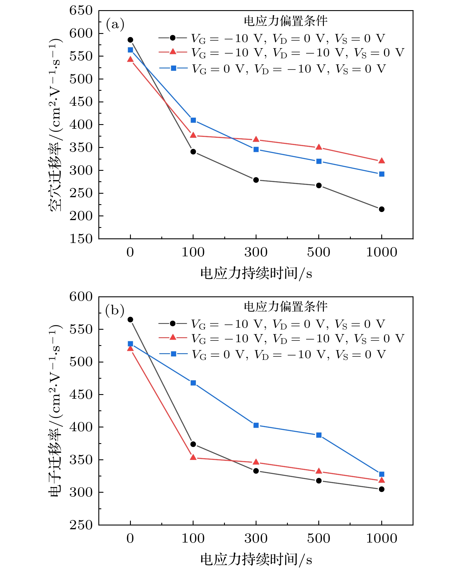
图 7 载流子迁移率随电应力累积时间的变化趋势 (a)空穴迁移率随电应力累积时间的变化趋势; (b)电子迁移率随电应力累积时间的变化趋势
Figure 7. The variations of carrier mobility with the accumulation time of electrical stress: (a) The variations of hole mobility with the accumulation time of electrical stress; (b) the variations of electron mobility with the accumulation time of electrical stress.
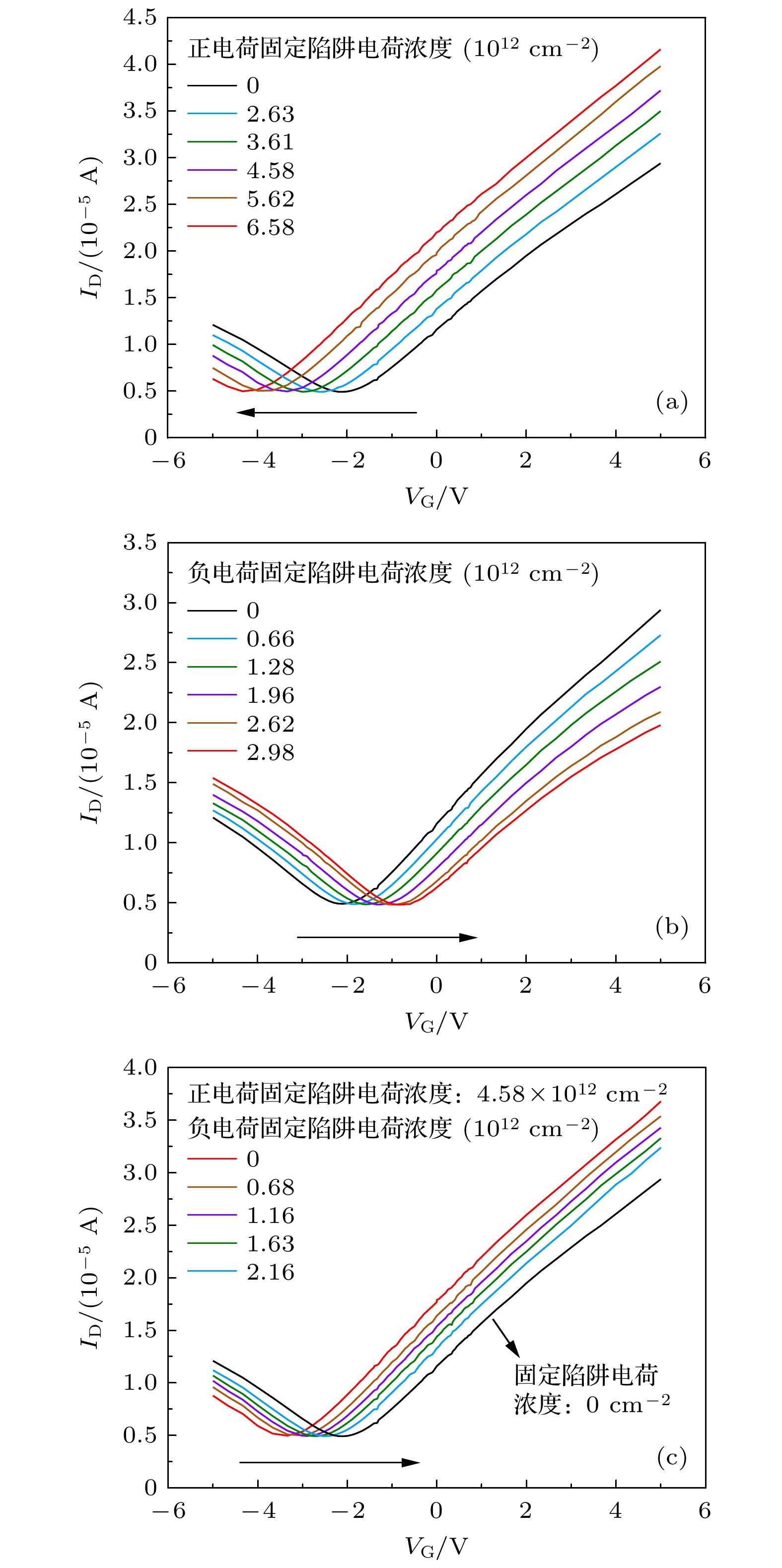
图 8 TCAD仿真结果 (a)带正电荷的固定陷阱电荷对GFET转移特性曲线的影响; (b)带负电荷的固定陷阱电荷对GFET转移特性曲线的影响; (c)带正电荷和带负电荷的固定陷阱电荷同时对GFET转移特性曲线的影响
Figure 8. TCAD simulation results: (a) Effect of a positively charged fixed trap charge on the transfer characteristic curve of GFET device; (b) effect of negatively charged fixed trap charge on the transfer characteristic curve of GFET device; (c) the effect of both positively charged and negatively charged fixed trap charges on the transfer characteristic curve of GFET devices.
表 1 电应力实验测试条件
Table 1. Electrical stress test conditions.
偏置电压条件 电应力测试时间点 转移特性曲线测试条件 栅极电应力(VG = –10 V, VD = 0 V, VS = 0 V) 0 s, 100 s, 300 s,
500 s, 1000 sVG 从–5 V扫到5 V,
VD 为20 mV, VS 接地漏极电应力 (VG = 0 V, VD = –10 V, VS = 0 V) 栅极电压与漏极电压同时施加的电应力
(VD = –10 V, VD = –10 V, VS = 0 V) -
[1] Novoselov K S, Geim A K, Morozov S V, Jiang D, Zhang Y, Dubonos S V, Grigorieva I V, Firsov A A 2004 Science 306 666
 Google Scholar
[2] 陈智, 王子欧, 李亦清, 李有忠, 毛凌锋 2012 微电子学与计算机 29 154
Chen Z, Wang Z O, Li Y Q, Li Y Z, Mao L F 2012 Microelectron. Comput. 29 154
[3] Radsar T, Khalesi H, Ghods V 2021 Superlattices Microstruct. 153 106869
 Google Scholar
[4] Zhang Q W 2018 Ph. D. Dissertation(Chengdu: University of Electronic Science and Technology of China) (in Chinese)[张庆伟 2018 博士学位论文 (成都: 电子科技大学)]
[5] Xu J, Gu Z Y, Yang W X, Wang Q L, Zhang X B 2018 Nanoscale Res. Lett. 13 311
 Google Scholar
[6] Yavari F, Kritzinger C, Gaire C, Song L, Gulapalli H, Borca-Tasciuc T, Ajayan P M, Koratkar N 2010 Small 6 2535
 Google Scholar
[7] Docherty C J, Lin C T, Joyce H J, Nicholas R J, Herz L M, Li L J, Johnston M B 2012 Nat. Commun. 3 1228
 Google Scholar
[8] Wang R, Wang S, Zhang D D, Li Z J, Fang Y, Qiu X H 2011 ACS Nano 5 408
 Google Scholar
[9] Feng T T, Xie D, Li G, Xu J L, Zhao H M, Ren T L, Zhu H W 2014 Carbon 78 250
 Google Scholar
[10] 张庆伟, 李平, 王刚, 曾荣周, 王恒, 周金浩 2017 微电子学与计算机 34 36
Zhang Q W, Li P, Wang G, Zeng R Z, Wang H, Zhou J H 2017 Microelectron. Comput. 34 36
[11] Ghosh S, Arroyo M 2013 J. Mech. Phys. Solids 61 235
 Google Scholar
[12] Zhao P, Chauhan J, Guo J 2009 Nano Lett. 9 684
 Google Scholar
[13] 陈卫 2017 博士学位论文 (长沙: 国防科技大学)
Cheng W 2017 Ph. D. Dissertation (Chang Sha: National University of Defense Technology
[14] Liu P, Wei Y, Jiang K L, Sun Q, Zhang X B, Fan S S, Zhang S F, Ning C G, Deng J K 2006 Phys. Rev. B 73 235412
 Google Scholar
[15] Li J, Zhang Z H, Wang D, Zhu Z, Fan Z Q, Tang G P, Deng X Q 2014 Carbon 69 142
 Google Scholar
[16] Chiu H Y, Perebeinos V, Lin Y M, Avouris P 2010 Nano Lett. 10 4634
 Google Scholar
[17] 李济芳, 郭红霞, 马武英, 宋宏甲, 钟向丽, 李洋帆, 白如雪, 卢小杰, 张凤祁 2024 73 058501
 Google Scholar
Li J F, Guo H X, Ma W Y, Song H J, Zhong X L, Li Y F, Bai R X, Lu X J, Zhang F Q 2024 Acta Phys. Sin. 73 058501
 Google Scholar
[18] Zhang Y F, Peng S Y, Wang Y H, Guo L X, Zhang X Y, Huang H Q, Su S H, Wang X W, Xue J M 2022 J. Phys. Chem. Lett. 13 10722
 Google Scholar
[19] Esqueda I S, Cress C D, Anderson T J, Ahlbin J R, Bajura M, Fritze M, Moon J S 2013 Electronics 2 234
 Google Scholar
[20] Kang C G, Lee Y G, Lee S K, Park E, Cho C, Lim S K, Hwang H J, Lee B H 2013 Carbon 53 182
 Google Scholar
[21] Petrosjanc K O, Adonin A S, Kharitonov I A, Sicheva M V 1994 Proceedings of 1994 IEEE International Conference on Microelectronic Test Structures 1994-03 pp126–129
[22] Galloway K F, Gaitan M, Russell T J 1984 IEEE Transactions on Nuclear Science 31 1497
 Google Scholar
[23] Jain S, Shinde V, Gajarushi A, Gupta A, Rao V R 2018 IEEE 13TH Nanotechnology Materials and Devices Conference (NMDC) New York, US October 14–17, 2018 pp353–356
[24] 谷文萍, 郝跃, 张进城, 王冲, 冯倩, 马晓华 2009 58 511
 Google Scholar
Gu W P, Hao Y, Zhang J C, Wang C, Feng Q, Ma X H 2009 Acta Phys. Sin. 58 511
 Google Scholar
[25] Childres I, Jauregui L A, Foxe M, Tian J, Jalilian R, Jovanovic I, Chen Y P 2010 Appl. Phys. Lett. 97 173109
 Google Scholar
[26] Ismail M A, Zaini K M M, Syono M I 2019 TELKOMNIKA (Telecommunication Computing Electronics and Control) 17 1845
 Google Scholar
[27] Jeppson K 2023 IEEE Trans. Electron Devices 70 1393
 Google Scholar
Catalog
Metrics
- Abstract views: 1696
- PDF Downloads: 46
- Cited By: 0


 DownLoad:
