


-
铁电负电容场效应晶体管可以突破传统金属氧化物半导体场效应晶体管中的玻尔兹曼限制, 将亚阈值摆幅降低到60 mV/dec以下, 极大地改善了晶体管的开关电流比和短沟道效应, 有效地降低了器件的功耗, 为实现晶体管特征尺寸的减小和摩尔定律的延续提供了选择. 本文分析总结了国内外近年来关于铁电负电容场效应晶体管代表性的研究进展, 为进一步研究提供参考. 首先介绍了铁电负电容场效应晶体管的研究背景及其意义; 然后总结了铁电材料的基本性质和种类, 并对铁电材料负电容的物理机制和铁电负电容场效应晶体管的工作原理进行了讨论; 接下来从器件沟道材料维度的角度, 分别总结了最近几年基于三维沟道材料和二维沟道材料且与氧化铪基铁电体结合的铁电负电容场效应晶体管的研究成果, 并对器件的亚阈值摆幅、开关电流比、回滞电压和漏电流等性能的改善进行了分析概述; 最后对铁电负电容场效应晶体管目前存在的问题和未来的发展方向作了总结与展望.
-
关键词:
- 铁电负电容场效应晶体管 /
- 氧化铪基铁电体 /
- 三维沟道材料 /
- 二维沟道材料
Ferroelectric negative capacitance field effect transistors(Fe-NCFETs) can break through the so-called “Boltzmann Tyranny” of traditional metal oxide semiconductor field effect transistors and reduce the subthreshold swing below 60 mV/dec, which could greatly improve the on/off current ratio and short-channel effect. Consequently, the power dissipation of the device is effectively lowered. The Fe-NCFET provides a choice for the downscaling of the transistor and the continuation of Moore’s Law. In this review, the representative research progress of Fe-NCFETs in recent years is comprehensively reviewed to conduce to further study. In the first chapter, the background and significance of Fe-NCFETs are introduced. In the second chapter, the basic properties of ferroelectric materials are introduced, and then the types of ferroelectric materials are summarized. Among them, the invention of hafnium oxide-based ferroelectric materials solves the problem of compatibility between traditional ferroelectric materials and CMOS processes, making the performance of NCFETs further improved. In the third chapter, the advantages and disadvantages of Fe-NCFETs with MFS, MFIS and MFMIS structures are first summarized, then from the perspective of atomic microscopic forces the “S” relationship curve of ferroelectric materials is derived and combined with Gibbs free energy formula and L-K equation, and the intrinsic negative capacitance region in the free energy curve of the ferroelectric material is obtained. Next, the steady-state negative capacitance and transient negative capacitance in the ferroelectric capacitor are discussed from the aspects of concept and circuit characteristics; after that the working area of negative capacitance Fe-NCFET is discussed. In the fourth chapter, the significant research results of Fe-NCFETs combined with hafnium-based ferroelectrics in recent years are summarized from the perspective of two-dimensional channel materials and three-dimensional channel materials respectively. Among them, the Fe-NCFETs based on three-dimensional channel materials such as silicon, germanium-based materials, III-V compounds, and carbon nanotubes are more compatible with traditional CMOS processes. The interface between the channel and the ferroelectric layer is better, and the electrical performance is more stable. However, thereremain some problems to be solved in three-dimensional channel materials such as the limited on-state current resulting from the low effective carrier mobility of the silicon, the small on/off current ratio due to the leakage caused by the small bandgap of the germanium-based material, the poor interfacial properties between the III-V compound materials and the dielectric layer, and the ambiguous working mechanism of Fe-NCFETs based on carbon nanotube. Compared with Fe-NCFETs based on three-dimensional channel materials, the Fe-NCFETs based on two-dimensional channel materials such as transition metal chalcogenide, graphene, and black phosphorus provide the possibility for the characteristic size of the transistor to be reduced to 3 nm. However, the interface performance between the two-dimensional channel material and the gate dielectric layer is poor, since there are numerous defect states at the interface. Furthermore, the two-dimensional channel materials have poor compatibility with traditional CMOS process. Hence, it is imperative to search for new approaches to finding a balance between device characteristics. Finally, the presently existing problems and future development directions of Fe-NCFETs are summarized and prospected.-
Keywords:
- ferroelectric negative capacitance field effect transistors /
- hafnia-based ferroelectrics /
- three-dimensional channel materials /
- two-dimensional channel materials
[1] Moore G E 1965 Electronics 38 114
[2] Mori K, Duong A, Richardson W F J 2002 IEEE T. Electron Dev. 49 61
 Google Scholar
[3] Fitzgerald E 2006 US Patent 11 412 262
[4] Chaudhry A, Kumar M J 2004 IEEE T. Device Ma. Re. 4 99
Google Scholar
[5] Tsutsui G, Saitoh M, Hiramoto T 2005 IEEE Electr. Device L. 26 836
Google Scholar
[6] Auth C, Allen C, Blattner A, Bergstrom D, Brazier M, Bost M, Buehler M, Chikarmane V, Ghani T, Glassman T 2012 Symposium on VLSI Technology Honolulu, HI, USA, June 12–14, 2012 p131
[7] Bae G, Bae D-I, Kang M, Hwang S, Kim S, Seo B, Kwon T, Lee T, Moon C, Choi Y 2019 IEEE International Electron Devices Meeting San Francisco, CA, USA, December 1–5, 2018 p28.7.1
[8] International Roadmap for Devices and Systems 2017 Edition Reports. https://irds.ieee.org/roadmap-2017 [2020-1-11].
[9] Zhirnov V V, Cavin R K 2008 Nat. Nanotechnol. 3 77
Google Scholar
[10] Woo Young C, Byung-Gook P, Jong Duk L, Tsu-Jae King L 2007 IEEE Electr. Device L. 28 743
Google Scholar
[11] Seabaugh A C, Zhang Q 2010 Proc. IEEE 98 2095
Google Scholar
[12] Ionescu A M, Riel H 2011 Nature 479 329
Google Scholar
[13] Mori T, Morita Y, Miyata N, Migita S, Fukuda K, Mizubayashi W, Masahara M, Yasuda T, Ota H 2015 Appl. Phys. Lett. 106 083501
Google Scholar
[14] Gopalakrishnan K, Griffin P B, Plummer J D 2003 Digest. International Electron Devices Meeting San Francisco, CA, USA, December 8–11, 2002 p289
[15] Kam H, Lee D T, Howe R T, King T J 2006 IEEE International Electron Devices Meeting, 2005. IEDM Technical Digest. Washington, DC, USA, December 5–5, 2005 p463
[16] Lefter M, Enachescu M, Voicu G R, Cotofana S D 2014 Proceedings of the 2014 IEEE/ACM International Symposium on Nanoscale Architectures Paris, France, July 15–17, 2014 p151
[17] Enachescu M, Lefter M, Voicu G R, Cotofana S D 2018 IEEE Trans. Emerg. Top. Comput. 6 184
Google Scholar
[18] Luong G V, Narimani K, Tiedemann A T, Bernardy P, Trellenkamp S, Zhao Q T, Mantl S 2016 IEEE Electr. Device L. 37 950
Google Scholar
[19] Kumar M J, Maheedhar M, Varma P P 2015 IEEE T. Electron Dev. 62 4345
Google Scholar
[20] Enachescu M, Voicu G R, Cotofana S D 2012 IEEE International Symposium on Circuits and Systems Seoul, South Korea, May 23–25, 2012 p2561
[21] Wei S, Zhang G, Liu J, Huang H, Geng L, Shao Z, Yang C F 2017 International Conference on Applied System Innovation (ICASI) Sapporo, Japan, May 13–17, 2017 p1293
[22] Colinge J P, Lee C W, Afzalian A, Akhavan N D, Yan R, Ferain I, Razavi P, O'Neill B, Blake A, White M, Kelleher A M, McCarthy B, Murphy R 2010 Nat. Nanotechnol. 5 225
Google Scholar
[23] Wang H, Han W, Li X, Zhang Y, Yang F 2014 J. Appl. Phys. 116 124505
Google Scholar
[24] Salahuddin S, Datta S J 2008 Nano Lett. 8 405
Google Scholar
[25] Zhou H, Kwon D, Sachid A B, Liao Y, Chatterjee K, Tan A J, Yadav A K, Hu C, Salahuddin S 2018 IEEE Symposium on VLSI Technology Honolulu, HI, USA, June 18–22, 2018 p53
[26] Kobayashi M 2018 Appl. Phys. Express 11 110101
Google Scholar
[27] Tan A J, Zhu Z, Choe H S, Hu C, Salahuddin S, Yoon A 2019 International Symposium on VLSI Technology, Systems and Application Hsinchu, Taiwan, China, April 22–25, 2019 p1
[28] Das S, Appenzeller J 2011 Nano Lett. 11 4003
Google Scholar
[29] Wang X, Yu P, Lei Z, Zhu C, Cao X, Liu F, You L, Zeng Q, Deng Y, Zhu C, Zhou J, Fu Q, Wang J, Huang Y, Liu Z 2019 Nat. Commun. 10 3037
Google Scholar
[30] Xu J, Jiang S Y, Zhang M, Zhu H, Chen L, Sun Q Q, Zhang D W 2018 Appl. Phys. Lett. 112 103104
Google Scholar
[31] Rusu A, Salvatore G A, Jiménez D, Ionescu A M 2010 International Electron Devices Meeting San Francisco, CA, USA, December 6–8, 2010 p16.3.1
[32] Hu C, Salahuddin S, Lin C I, Khan A 2015 73rd Annual Device Research Conference Columbus, OH, USA, June 21–24, 2015 p39
[33] McGuire F A, Lin Y C, Price K, Rayner G B, Khandelwal S, Salahuddin S, Franklin A D 2017 Nano Lett. 17 4801
Google Scholar
[34] Pahwa G, Agarwal A, Chauhan Y S 2018 IEEE T. Electron Dev. 65 5130
Google Scholar
[35] Mehta H, Kaur H 2019 4th International Conference on Devices, Circuits and Systems Coimbatore, India, March 16–17, 2018 p164
[36] Mehta H, Kaur H 2018 IEEE T. Electron Dev. 65 2699
Google Scholar
[37] Shao Q, Wang X, Jiang W, Chen Y, Zhang X, Tu L, Lin T, Shen H, Meng X, Liu A, Wang J 2019 Appl. Phys. Lett. 115 162902
Google Scholar
[38] Fan C C, Tu C Y, Lin M H, Chang C Y, Cheng C H, Chen Y L, Liou G L, Liu C, Chou W C, Hsu H H 2018 IEEE International Reliability Physics Symposium Burlingame, CA, USA, March 11–15, 2018 pP-TX.8-1
[39] 钟维烈 1996 铁电体物理学 (北京: 科学出版社) 第1页
Zhong W L 1996 Ferroelectric Physics (Beijing: Science Press) p1 (in Chinese)
[40] Kholkin A L, Pertsev N A, Goltsev A V 2008 Piezoelectricity and Crystal Symmetry (Boston: Springer US) pp28–29
[41] Koh J H 2002 Ph. D. Dissertation (Stockholm: Royal Institute of Technology)
[42] Wersing W, Bruchhaus R 2000 Pyroelectric Devices and Applications (Cambridge: Academic Press) p143
[43] Sawaguchi E, Akishige Y, Kobayashi M 1985 J. Phys. Soc. Jpn. 54 480
Google Scholar
[44] Lu S W, Lee B I, Wang Z L, Samuels W D 2000 J. Cryst. Growth 219 269
Google Scholar
[45] Smith M B, Page K, Siegrist T, Redmond P L, Walter E C, Seshadri R, Brus L E, Steigerwald M L 2008 J. Am. Chem. Soc. 130 6955
Google Scholar
[46] Valasek J 1921 Phys. Rev. 17 475
Google Scholar
[47] Ploss B, Ploss B, Shin F G, Chan H L, Choy C L 2000 IEEE Trns. Dielectr. Electr. Insul. 7 517
Google Scholar
[48] Nguyen C A, Mhaisalkar S G, Ma J, Lee P S 2008 Org. Electron. 9 1087
Google Scholar
[49] Kang S J, Park Y J, Bae I, Kim K J, Kim H C, Bauer S, Thomas E L, Park C 2009 Adv. Funct. Mater. 19 2812
Google Scholar
[50] Jo J, Choi W Y, Park J D, Shim J W, Yu H Y, Shin C 2015 Nano Lett. 15 4553
Google Scholar
[51] Zhang W, Xiong R G 2012 Chem. Rev. 112 1163
Google Scholar
[52] Liu Y L, Ge J Z, Wang Z X, Xiong R G 2019 Inorg. Chem. Front. 7 128
Google Scholar
[53] Ikeda T, Sasaki T, Ichimura K 1993 Nature 361 428
Google Scholar
[54] Zhang H, Chen Y, Ding S, Wang J, Bao W, Zhang D W, Zhou P 2018 Nanotechnology 29 244004
Google Scholar
[55] Beresnev L A, Chigrinov V G, Dergachev D I, Poshidaev E P, Fünfschilling J, Schadt M 1989 Liq. Cryst. 5 1171
Google Scholar
[56] Ye H Y, Tang Y Y, Li P F, Liao W Q, Gao J X, Hua X N, Cai H, Shi P P, You Y M, Xiong R G J S 2018 Science 361 151
Google Scholar
[57] Li P F, Liao W Q, Tang Y Y, Qiao W, Zhao D, Ai Y, Yao Y F, Xiong R G 2019 Proc. Natl. Acad. Sci. U S.A 116 5878
Google Scholar
[58] Li L, Wu M 2017 ACS Nano 11 6382
Google Scholar
[59] Ding W, Zhu J, Wang Z, Gao Y, Xiao D, Gu Y, Zhang Z, Zhu W 2017 Nat. Commun. 8 14956
Google Scholar
[60] Li Y, Gong M, Zeng H 2019 J. Semicond. 40 061002s
Google Scholar
[61] Liu F, You L, Seyler K L, Li X, Yu P, Lin J, Wang X, Zhou J, Wang H, He H, Pantelides S T, Zhou W, Sharma P, Xu X, Ajayan P M, Wang J, Liu Z 2016 Nat. Commun. 7 12357
Google Scholar
[62] Wu M, Jena P 2018 Wiley Interdiscip. Rev.-Comput. Mol. Sci. 8 1365
Google Scholar
[63] Böscke T S, Müller J, Bräuhaus D, Schröder U, Böttger U 2011 Appl. Phys. Lett. 99 102903
Google Scholar
[64] Mueller S, Mueller J, Singh A, Riedel S, Sundqvist J, Schroeder U, Mikolajick T 2012 Adv. Funct. Mater. 22 2412
Google Scholar
[65] Müller J, Schröder U, Böscke T S, Müller I, Böttger U, Wilde L, Sundqvist J, Lemberger M, Kücher P, Mikolajick T, Frey L 2011 J. Appl. Phys. 110 114113
Google Scholar
[66] Starschich S, Boettger U 2017 J. Mater. Chem. C 5 333
Google Scholar
[67] Schroeder U, Mueller S, Mueller J, Yurchuk E, Martin D, Adelmann C, Schloesser T, van Bentum R, Mikolajick T 2013 ECS J. Solid State Sci. Technol. 2 N69
Google Scholar
[68] Schroeder U, Yurchuk E, Müller J, Martin D, Schenk T, Polakowski P, Adelmann C, Popovici M I, Kalinin S V, Mikolajick T 2014 Jpn. J. Appl. Phys. 53 08LE02
Google Scholar
[69] Müller J, Böscke T S, Bräuhaus D, Schröder U, Böttger U, Sundqvist J, Kücher P, Mikolajick T, Frey L 2011 Appl. Phys. Lett. 99 112901
Google Scholar
[70] Müller J, Boscke T S, Schroder U, Mueller S, Brauhaus D, Bottger U, Frey L, Mikolajick T 2012 Nano Lett. 12 4318
Google Scholar
[71] Terki R, Bertrand G, Aourag H, Coddet C 2008 Mater. Lett. 62 1484
Google Scholar
[72] Íñiguez J, Zubko P, Luk’yanchuk I, Cano A 2019 Nat. Rev. Mater. 4 243
Google Scholar
[73] Sayeef S, Supriyo D 2008 Nano Letter 8 405
[74] Lu P S, Lin C C, Su P 2019 International Symposium on VLSI Technology, Systems and Application Hsinchu, Taiwan, China, April 22–25, 2019 p1
[75] Muller J, Boscke T S, Schroder U, Hoffmann R, Mikolajick T, Frey L 2012 IEEE Electr. Device L. 33 185
Google Scholar
[76] Pahwa G, Dutta T, Agarwal A, Chauhan Y S 2017 IEEE T. Electron Dev. 64 1366
Google Scholar
[77] Park B E, Lee G G 2010 J. Korean Phys. Soc. 56 1484
Google Scholar
[78] Sun J, Zheng X 2011 IEEE T. Electron Dev. 58 3559
Google Scholar
[79] Sun J, Zheng X J, Li W 2012 Curr. Appl. Phys. 12 760
Google Scholar
[80] Jang K, Kobayashi M, Hiramoto T 2018 Jpn. J. Appl. Phys. 57 114202
Google Scholar
[81] Li Y, Lian Y, Samudra G S 2015 Semicond. Sci. Technol. 30 045011
Google Scholar
[82] Sun J, Li Y, Cao L 2019 J. Comput. Electron. 18 527
Google Scholar
[83] Hoffmann M, Pesic M, Slesazeck S, Schroeder U, Mikolajick T 2018 Nanoscale 10 10891
Google Scholar
[84] Cheng C H, Fan C C, Tu C Y, Hsu H H, Chang C Y 2019 IEEE T. Electron Dev. 66 825
Google Scholar
[85] Wong J C, Salahuddin S 2019 Proc. IEEE 107 49
Google Scholar
[86] Luttinger J M, Tisza L 1946 Phys. Rev. 70 954
Google Scholar
[87] Slater J C 1950 Phys. Rev. 78 748
Google Scholar
[88] Islam Khan A, Bhowmik D, Yu P, Joo Kim S, Pan X, Ramesh R, Salahuddin S 2011 Appl. Phys. Lett. 99 113501
Google Scholar
[89] Rabe K M, Dawber M, Lichtensteiger C, Ahn C H, Triscone J-M 2007 Physics of Ferroelectrics: A Modern Perspective (Berlin, Heidelberg: Springer Berlin Heidelberg) pp1–30
[90] Gao W, Khan A, Marti X, Nelson C, Serrao C, Ravichandran J, Ramesh R, Salahuddin S 2014 Nano Lett. 14 5814
Google Scholar
[91] Alam M A, Si M, Ye P D 2019 Appl. Phys. Lett. 114 090401
Google Scholar
[92] Liu Z, Bhuiyan M, Ma T 2019 IEEE International Electron Devices Meeting San Francisco, CA, USA, December 1–5, 2018 p31.2.1
[93] Hoffmann M, Slesazeck S, Mikolajick T, Hwang C S 2019 Ferroelectricity in Doped Hafnium Oxide: Materials, Properties and Devices (Cambridge: Woodhead Publishing) p473
[94] Khan A I, Chatterjee K, Wang B, Drapcho S, You L, Serrao C, Bakaul S R, Ramesh R, Salahuddin S 2015 Nat. Mater. 14 182
Google Scholar
[95] Jang K, Ueyama N, Kobayashi M, Hiramoto T 2018 IEEE J. Electron Devices Soc. 6 346
Google Scholar
[96] Kim K D, Kim Y J, Park M H, Park H W, Kwon Y J, Lee Y B, Kim H J, Moon T, Lee Y H, Hyun S D, Kim B S, Hwang C S 2019 Adv. Funct. Mater. 29 1808228
Google Scholar
[97] Han Q, Aleksa P, Tromm T C U, Schubert J, Mantl S, Zhao Q T 2019 Solid-State Electron. 159 71
Google Scholar
[98] Catalan G, Jiménez D, Gruverman A 2015 Nat. Mater. 14 137
Google Scholar
[99] Chang S C, Avci U E, Nikonov D E, Manipatruni S, Young I A 2018 Phys. Rev. Appl. 9 014010
Google Scholar
[100] Landau L, Khalatnikov I 1954 Dokl. Akad. Nauk SSSR. 96 469
Google Scholar
[101] Hoffmann M, Khan A I, Serrao C, Lu Z, Salahuddin S, Pešić M, Slesazeck S, Schroeder U, Mikolajick T 2018 J. Appl. Phys. 123 184101
Google Scholar
[102] Merz W J 1954 Phys. Rev. 95 690
Google Scholar
[103] Chang S-C, Avci U E, Nikonov D E, Young I A 2017 IEEE J. Explor. Solid-State Comput. Devices Circuits 3 56
Google Scholar
[104] Jin C, Saraya T, Hiramoto T, Kobayashi M 2019 IEEE J. Electron Devices Soc. 7 368
Google Scholar
[105] Wang H, Yang M, Huang Q, Zhu K, Zhao Y, Liang Z, Chen C, Wang Z, Zhong Y, Zhang X 2019 IEEE International Electron Devices Meeting San Francisco, CA, USA, December 1–5, 2018 p31.1.1
[106] Orihara H, Hashimoto S, Ishibashi Y 1994 J. Phys. Soc. Jpn. 63 1031
Google Scholar
[107] Jo J, Shin C 2016 IEEE Electr. Device L. 37 245
Google Scholar
[108] Nourbakhsh A, Zubair A, Joglekar S, Dresselhaus M, Palacios T 2017 Nanoscale 9 6122
Google Scholar
[109] Saeidi A, Jazaeri F, Bellando F, Stolichnov I, Enz C C, Ionescu A M 2017 47th European Solid-State Device Research Conference Leuven, Belgium, September 11–14, 2017 p78
[110] Galatage R, Bentley S, Suvarna P H, Krivokapic Z 2018 US Patent 10 141 414 B1
[111] Khan A I, Yeung C W, Hu C, Salahuddin S 2012 International Electron Devices Meeting Washington, DC, USA, December 5–7, 2011 p11.3.1
[112] Agarwal H, Kushwaha P, Lin Y K, Kao M Y, Liao Y H, Dasgupta A, Salahuddin S, Hu C 2019 IEEE Electr. Device L. 40 463
Google Scholar
[113] Si M, Su C J, Jiang C, Conrad N J, Zhou H, Maize K D, Qiu G, Wu C T, Shakouri A, Alam M A, Ye P D 2018 Nat. Nanotechnol. 13 24
Google Scholar
[114] Bohr M T, Young I A 2017 IEEE Micro 37 20
[115] Cheng C H, Chin A 2014 IEEE Electr.Device L. 35 274
Google Scholar
[116] Fan CC, Cheng CH, Chen YR, Liu C, Chang CY 2018 IEEE International Electron Devices Meeting San Francisco, CA, USA, December 2–6, 2017 p23.2.1
[117] Chiu YC, Cheng CH, Chang C-, Tang YT, Chen MC 2016 IEEE Symposium on VLSI Technology Honolulu, HI, USA, June 14–16, 2016 p1
[118] Cheng CH, Fan CC, Hsu HH, Wang SA, Chang CY 2019 Phys. Status Solidi-Rapid Res. Lett. 13 1800493
Google Scholar
[119] Cheng C H, Lin M H, Chen H Y, Fan C C, Liu C, Hsu H H, Chang C Y 2018 Phys. Status Solidi-Rapid Res. Lett. 13 1800573
Google Scholar
[120] Zeng B, Xiao W, Liao J, Liu H, Liao M, Peng Q, Zheng S, Zhou Y 2018 IEEE Electr. Device L. 39 1508
Google Scholar
[121] Chen K T, Liao C Y, Chen H Y, Lo C, Siang G Y, Lin Y Y, Tseng Y J, Chang C, Chueh C Y, Yang Y J, Liao M H, Li K S, Chang S T, Lee M H 2019 Microelectron. Eng. 215 110991
Google Scholar
[122] Xiao W, Liu C, Peng Y, Zheng S, Feng Q, Zhang C, Zhang J, Hao Y, Liao M, Zhou Y 2019 IEEE Electr. Device L. 40 714
Google Scholar
[123] Li K S, Chen P G, Lai T Y, Lin C H, Cheng C C, Chen C C, Wei Y J, Hou Y F, Liao M H, Lee M H 2016 IEEE International Electron Devices Meeting Washington, DC, USA, December 7–9, 2015 p22.6.1
[124] Zhang Z, Xu G, Zhang Q, Hou Z, Li J, Kong Z, Zhang Y, Xiang J, Xu Q, Wu Z, Zhu H, Yin H, Wang W, Ye T 2019 IEEE Electr. Device L. 40 367
Google Scholar
[125] Chen P J, Tsai M J, Hou F J, Wu Y C 2019 Silicon Nanoelectronics Workshop Kyoto, Japan, June 9–10, 2019 p1
[126] Lee S Y, Chen H W, Shen C H, Kuo P Y, Chung C C, Huang Y E, Chen H Y, Chao T S 2019 IEEE Electr. Device L. 40 1708
Google Scholar
[127] Bansal A K, Kumar M, Gupta C, Hook T B, Dixit A 2018 IEEE T. Electron Dev. 65 3548
Google Scholar
[128] Song Y, Zhou H, Xu Q, Luo J, Yin H, Yan J, Zhong H 2011 J. Electron. Mater. 40 1584
Google Scholar
[129] Zhou J, Han G, Li Q, Peng Y, Lu X, Zhang C, Zhang J, Sun QQ, Zhang D W, Hao Y 2017 IEEE International Electron Devices Meeting San Francisco, CA, USA, December 3–7, 2016 p12.2.1
[130] Zhou J, Han G, Peng Y, Liu Y, Zhang J, Sun Q Q, Zhang D W, Hao Y 2017 IEEE Electr. Device L. 38 1157
Google Scholar
[131] Li J, Zhou J, Han G, Liu Y, Peng Y, Zhang J, Sun Q Q, Zhang D W, Hao Y 2017 IEEE Electr. Device L. 38 1500
Google Scholar
[132] Zhou J, Han G, Li J, Liu Y, Peng Y, Zhang J, Sun Q Q, Zhang D W, Hao Y 2018 IEEE Electr.Device L. 39 622
Google Scholar
[133] Zhou J, Han G, Li J, Liu Y, Peng Y, Zhang J, Sun Q Q, Zhang D W, Hao Y 2018 IEEE Electr. Device L. 39 618
Google Scholar
[134] Peng Y, Liu Y, Han G, Zhang J, Hao Y 2019 Nanoscale Res. Lett. 14 125
Google Scholar
[135] Alghamdi S, Chung W, Si M, Peide D Y 2018 76th Device Research Conference Santa Barbara, CA, USA, June 24–27, 2018 p1
[136] Luc Q, Fan-Chiang C, Huynh S, Huang P, Do H, Ha M, Jin Y, Nguyen T, Zhang K, Wang H 2018 IEEE Symposium on VLSI Technology Honolulu, HI, USA, June 18–22, 2018 p47
[137] Chang E Y, Luc Q H, Tran N A, Lin Y C 2019 ECS Trans. 92 3
Google Scholar
[138] Srimani T, Hills G, Bishop M D, Radhakrishna U, Zubair A, Park R S, Stein Y, Palacios T, Antoniadis D, Shulaker M M 2018 IEEE Electr. Device L. 39 304
Google Scholar
[139] Tu L, Wang X, Wang J, Meng X, Chu J 2018 Adv. Electron. Mater. 4 1800231
Google Scholar
[140] Si M, Jiang C, Chung W, Du Y, Alam M A, Ye P D 2018 Nano Lett. 18 3682
Google Scholar
[141] Lee Y T, Kwon H, Kim J S, Kim H H, Lee Y J, Lim J A, Song YW, Yi Y, Choi WK, Hwang D K 2015 ACS Nano 9 10394
Google Scholar
[142] Heidler J, Yang S, Feng X, Müllen K, Asadi K 2018 Solid-State Electron. 144 90
Google Scholar
[143] Choi H, Shin C 2019 Phys. Status Solidi A 216 1900177
Google Scholar
[144] Yu Z, Wang H, Li W, Xu S, Song X, Wang S, Wang P, Zhou P, Shi Y, Chai Y 2018 IEEE International Electron Devices Meeting San Francisco, CA, USA, December 2-6, 2017 p23.6.1
[145] Yap W C, Jiang H, Liu J, Xia Q, Zhu W 2017 Appl. Phys. Lett. 111 013103
Google Scholar
[146] McGuire F A, Lin Y C, Rayner B, Franklin A D 2017 75th Annual Device Research Conference South Bend, IN, USA, June 25–28, 2017 p1
[147] Alghamdi S, Si M, Yang L, Peide D Y 2018 IEEE International Reliability Physics Symposium Burlingame, CA, USA, March 11–15, 2018 pP-TX.1-1
[148] Wang J, Guo X, Yu Z, Ma Z, Liu Y, Chan M, Zhu Y, Wang X, Chai Y 2019 IEEE International Electron Devices Meeting San Francisco, CA, USA, December 1–5, 2018 p22.3.1
[149] Si M, Peide D Y 2018 International Symposium on VLSI Technology, Systems and Application Hsinchu, Taiwan, April 16–19, 2018 p1
[150] Liu F, Zhou Y, Wang Y, Liu X, Wang J, Guo H 2016 NPJ Quantum Mater. 1 16004
Google Scholar
[151] Park N, Kang H, Park J, Lee Y, Yun Y, Lee J H, Lee S G, Lee Y H, Suh D 2015 ACS Nano 9 10729
Google Scholar
[152] Jie W, Hao J 2017 Nanoscale 10 328
[153] Lipatov A, Fursina A, Vo T H, Sharma P, Gruverman A, Sinitskii A 2017 Adv. Electron. Mater. 3 1700020
Google Scholar
[154] Lee Y, Jeon W, Cho Y, Lee M H, Jeong S J, Park J, Park S 2016 ACS Nano 10 6659
Google Scholar
[155] Tian H, Li Y-x, Li L, Wang X, Liang R, Yang Y, Ren T L 2019 IEEE T. Electron Dev. 66 1579
Google Scholar
[156] Li J, Liu Y, Han G, Zhou J, Hao Y 2019 Nanoscale Res. Lett. 14 171
Google Scholar
[157] Peng Y, Han G, Xiao W, Wu J, Liu Y, Zhang J, Hao Y 2019 Nanoscale Res. Lett. 14 115
Google Scholar
[158] Tokumitsu E 2020 Jpn. J. Appl. Phys. 59 SCCB06
Google Scholar
[159] Park J H, Jang G S, Kim H Y, Seok K H, Chae H J, Lee S K, Joo S K 2016 Sci. Rep. 6 24734
Google Scholar
[160] Lee M H, Fan S T, Tang C H, Chen P G, Chou Y C, Chen H H, Kuo J Y, Xie M J, Liu S N, Liao M H 2017 IEEE International Electron Devices Meeting San Francisco, CA, USA, December 3–7, 2016 p12.1.1
[161] Zhang X D, Han W H, Liu W, Zhao X S, Guo Y Y, Yang C, Chen J D, Yang F H 2019 Chin. Phys. B 28 127302
Google Scholar
[162] Guo Y Y, Han W H, Zhao X S, Dou Y M, Zhang X D, Wu X Y, Yang F H 2019 Chin. Phys. B 28 107303
Google Scholar
[163] Zhao X S, Han W H, Guo Y Y, Dou Y M, Yang F H 2018 Chin. Phys. B 27 097310
Google Scholar
-

图 4 有机钙钛矿A(NH4)X3家族化学和晶格结构[56] (a) 有机钙钛矿铁电体的三维化学结构组成图; (b) 铁电相MDABCO-NH4I3在293 K时的晶胞结构图, 右侧椭圆中为有机正离子的空间结构示意图, 其对称性接近于球体; (c) 铁电相MDABCO-NH4I3在463 K时的晶胞结构图
Fig. 4. Chemical and crystal structures of the metal-free A(NH4) X3 family[56]: (a) Chemical structures of constituents of the metal-free 3D perovskite ferroelectrics; (b) the packing diagram of MDABCO–NH4I3 in the ferroelectric phase at 293 K. The oval to the right contains the space-fill diagram of the organic cation, showing the cationic geometry to be close to a ball; (c) the packing diagram of MDABCO–NH4I3 in the paraelectric phase at 463 K.
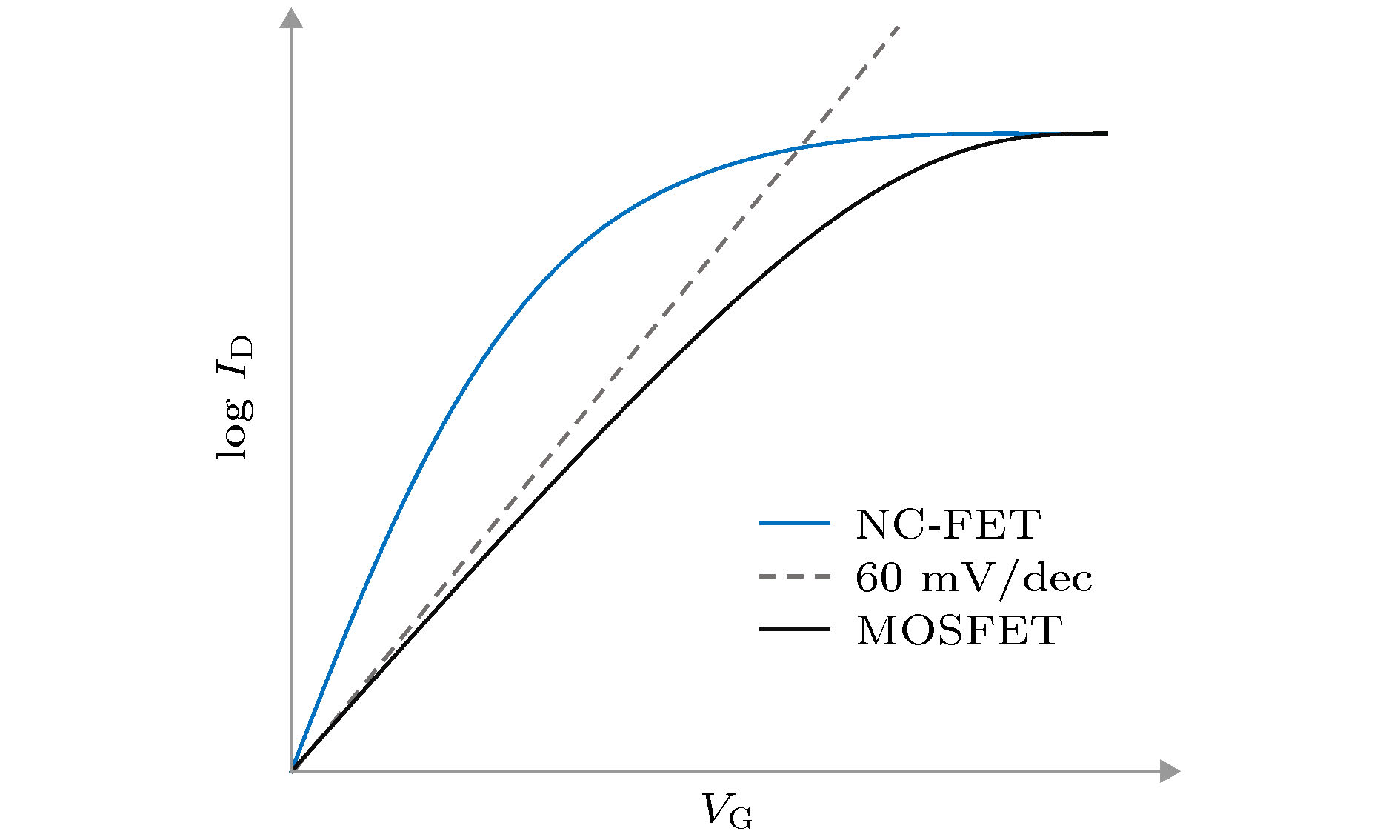
图 5 场效应晶体管转移特性曲线
Fig. 5. The transfer characteristic curve of field effect transistors.


图 7 器件结构图 (a) 传统MOSFETs; (b) MFIS; (c) MFMIS
Fig. 7. Device structure diagram: (a) Traditional MOSFETs; (b) MFIS; (c) MFMIS.
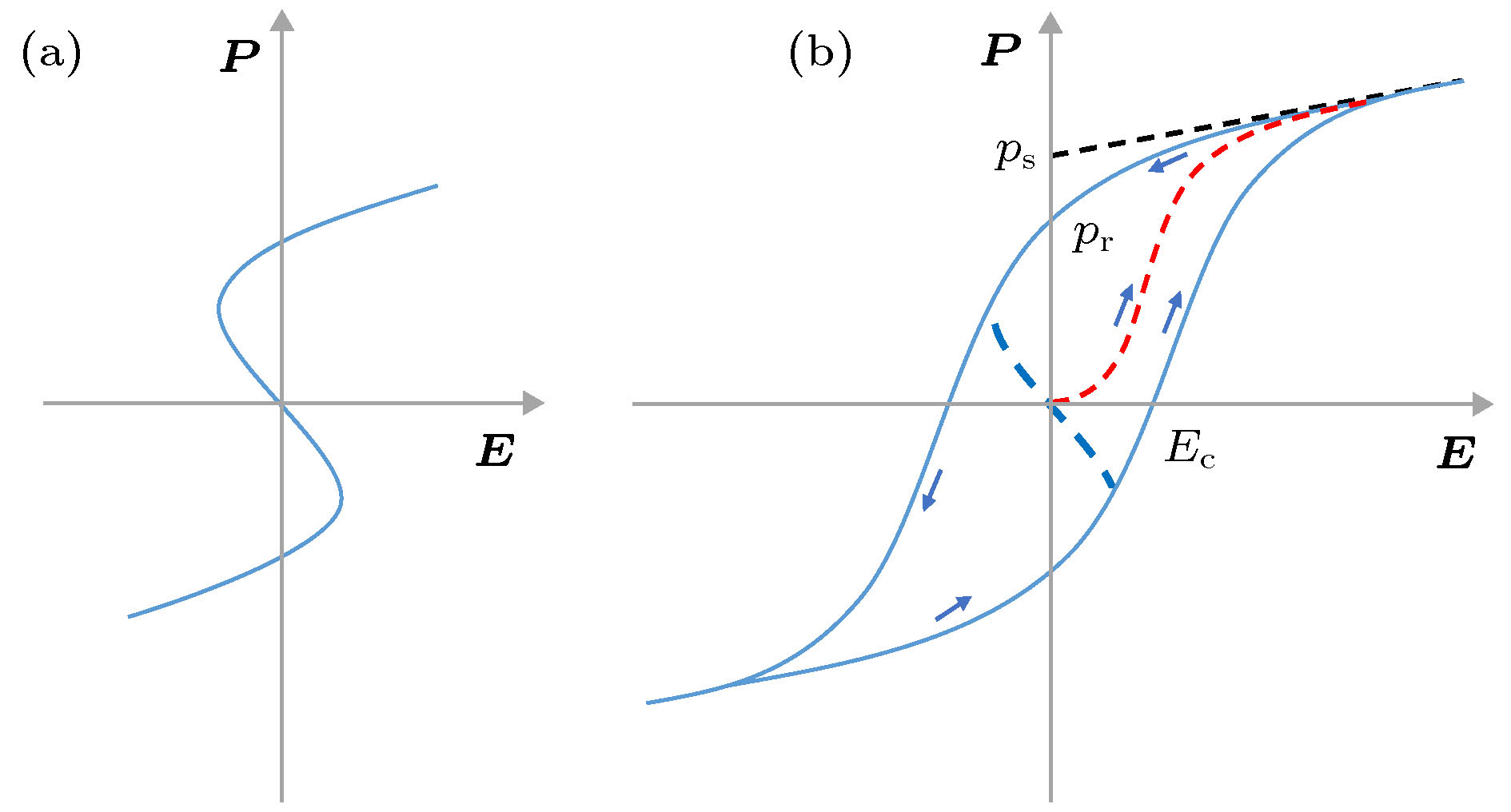
图 9 铁电体极化强度P和电场E之间的关系 (a) P-E关系图; (b) 电滞回线图
Fig. 9. The relationship between polarization P and electric field E of ferroelectrics: (a) P vs. E; (b) hysteresis diagram.

图 10 (a) 铁电体的QFE-VFE关系图; (b)铁电体的UFE-QFE关系图
Fig. 10. (a) QFE vs. VFE of ferroelectrics; (b) UFE vs. QFE of ferroelectrics.
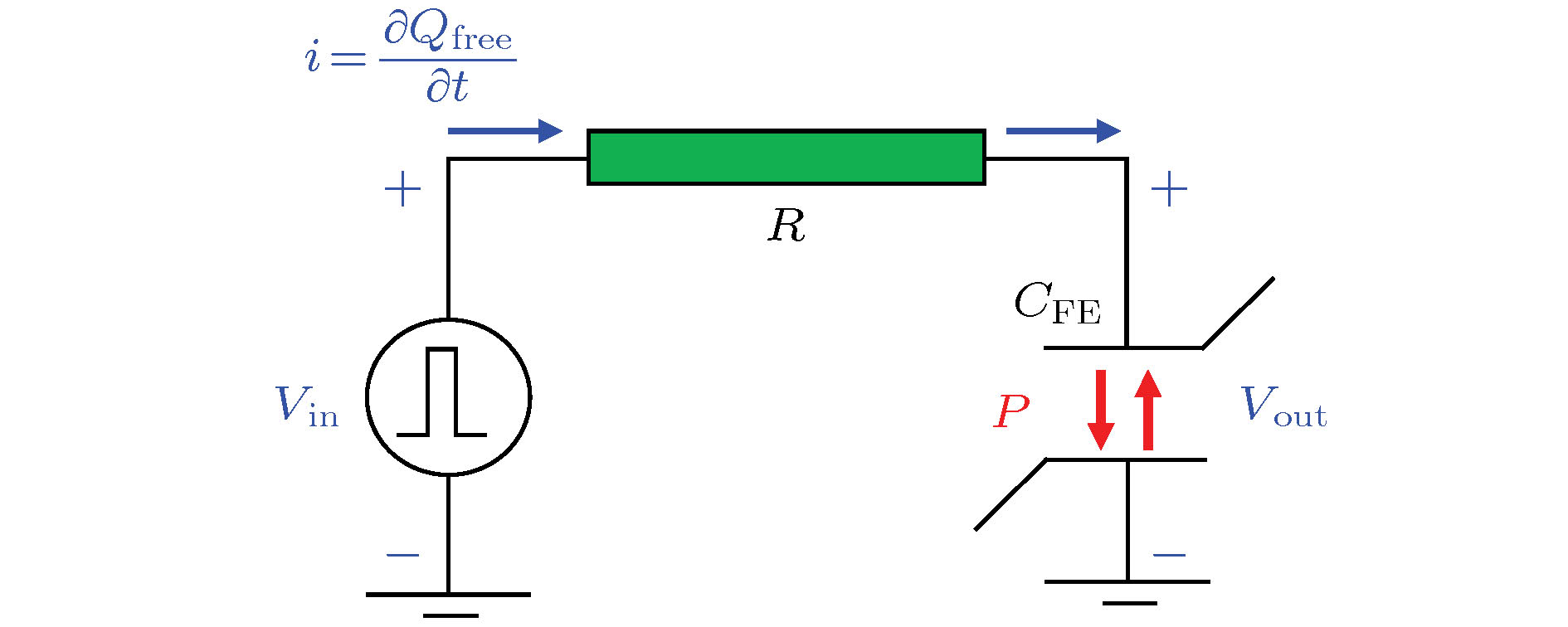
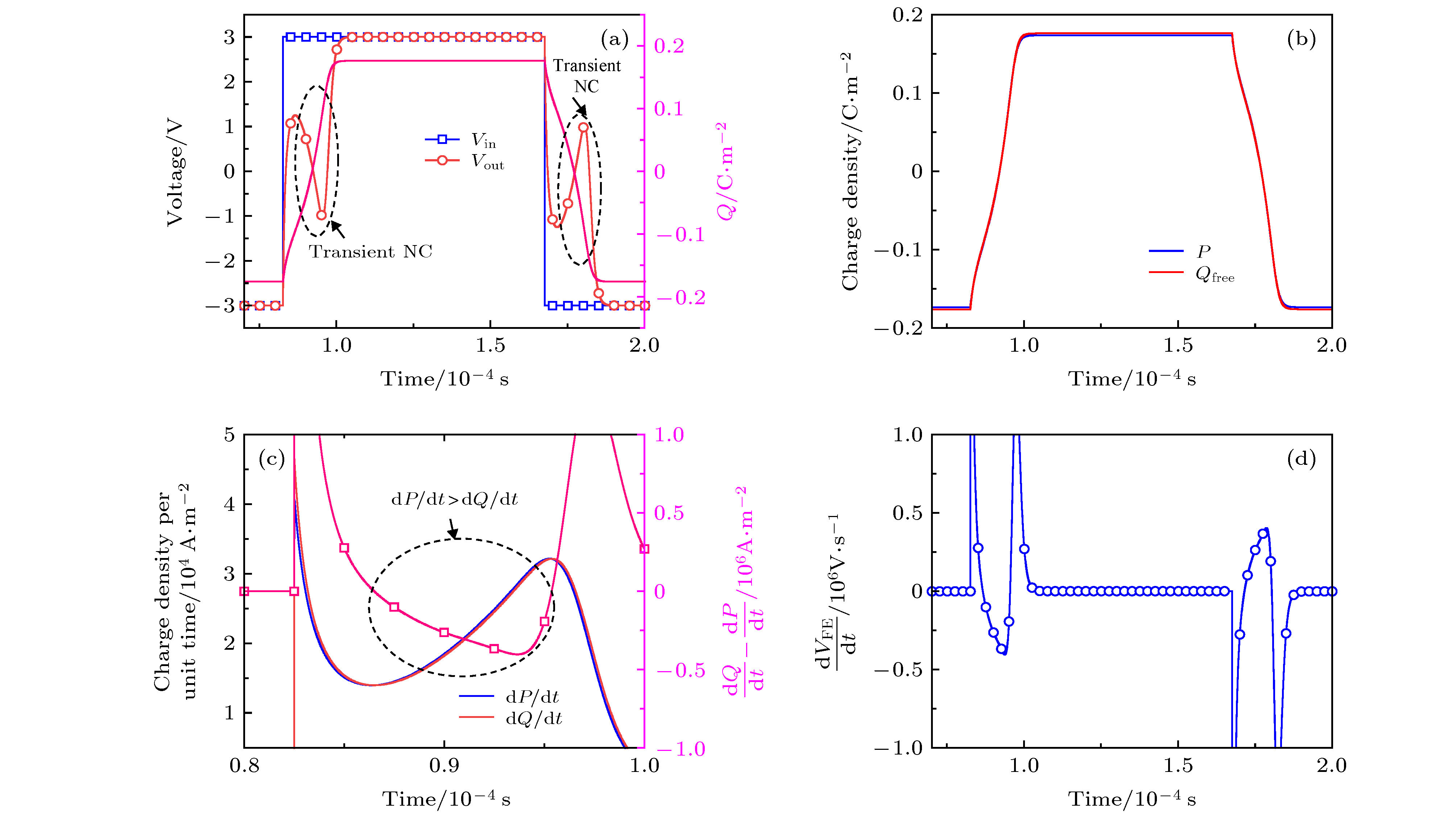
图 14 瞬态NC模拟结果[99] (a) 输入电压, 输出电压和铁电电容上自由电荷与时间的关系图; (b) 极化强度和自由电荷与时间的关系图; (c) 极化强度和自由电荷对时间的微分结果及其差值随时间的变化曲线; (d) 铁电电容电压的变化速度随时间的变化曲线
Fig. 14. The simulation results of transient NC[99]: (a) Input voltage, output voltage, and free charge on a ferroelectric capacitor as functions of time; (b) polarization and free charge as functions of time; (c) charge density per unit time for free charge and polarization and the difference between them; (d) change in the voltage across a ferroelectric capacitor per unit time as a function of time.

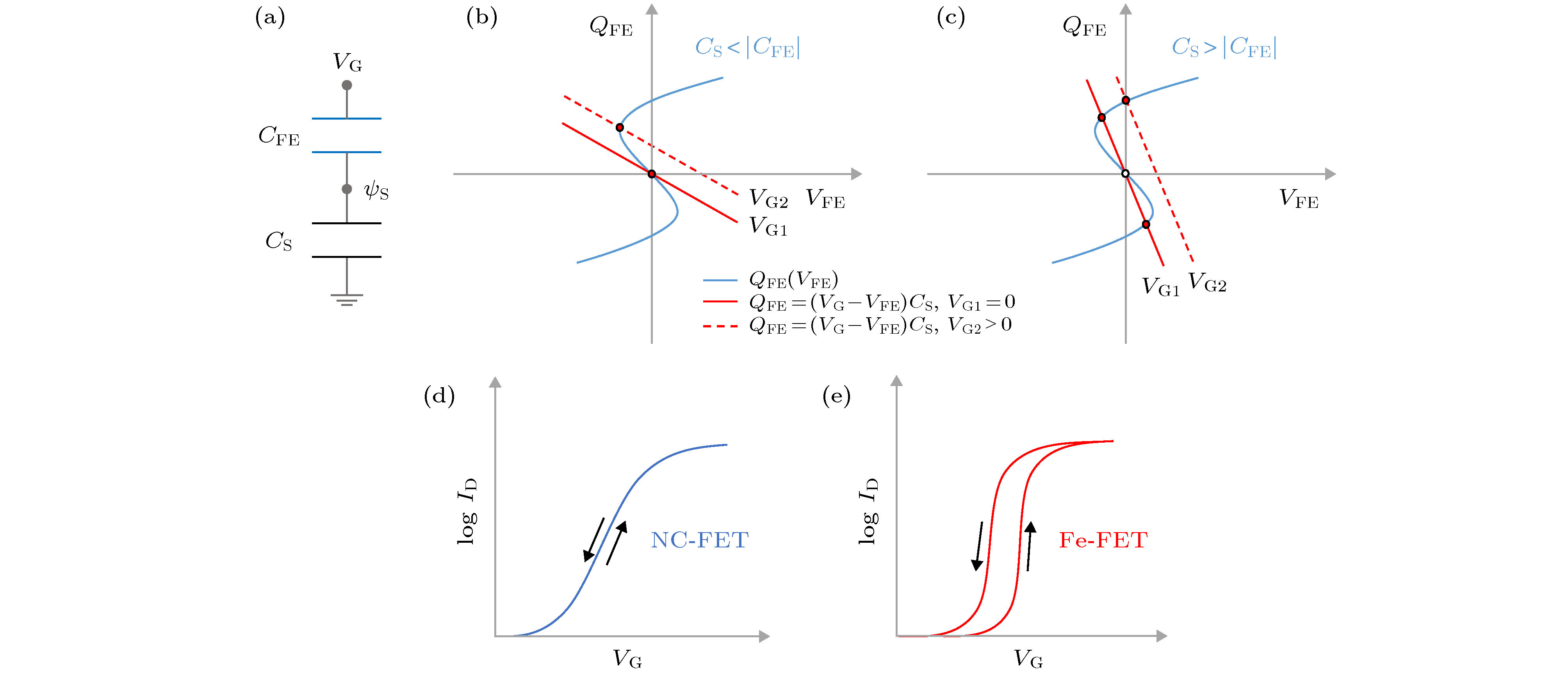
图 16 器件电容电荷量与电压的关系 (a) 电容模型; (b)
${C_{\rm{S}}} < \left| {{C_{{\rm{FE}}}}} \right|$ ; (c)${C_{\rm{S}}} < \left| {{C_{{\rm{FE}}}}} \right|$ ; (d) Fe-NCFETs[91]; (e) Fe-FET[91]Fig. 16. The relationship between capacitive charge and voltage of the device: (a) Capacitance model; (b)
${C_{\rm{S}}} < \left| {{C_{{\rm{FE}}}}} \right|$ ; (c)${C_{\rm{S}}} < \left| {{C_{{\rm{FE}}}}} \right|$ (d) Fe-NCFETs[91]; (e) Fe-FETs[91].
图 17 平面型硅基- HfAlO Fe-NCFETs[116] (a) 器件截面透射电子显微镜(transmission electron microscope, TEM)图; (b) 剩余极化强度与TaN中N含量的关系曲线; (c) F离子钝化作用对铁电层能带影响的示意图; (d) 不同处理作用后器件的SS与源漏电压的关系
Fig. 17. Planar Silicon based HfAlO Fe-NCFETs[116]: (a) HR TEM cross-section image; (b) polarization as a function of nitrogen content of TaN; (c) schematic band diagram of HfAlO before and after F-passivation; (d) SS as a function of VDS after different treatments.

图 18 硅基NCFinFET[123] (a) 器件截面TEM图; (b) 铁电NCFinFET的栅压放大系数与栅压的关系曲线; (c) 常规FinFET和铁电NCFinFET的SS与栅压的关系曲线
Fig. 18. Silicon based NC-FinFET[123]: (a) TEM cross-sectional image of NC-FinFET with TiN internal gate, HfZrO FE film and TiN gate; (b) the gate amplification coefficient as a function of VG for NC-FinFET; (c) SS as a function of VG for conventional FinFET and NC-FinFET.
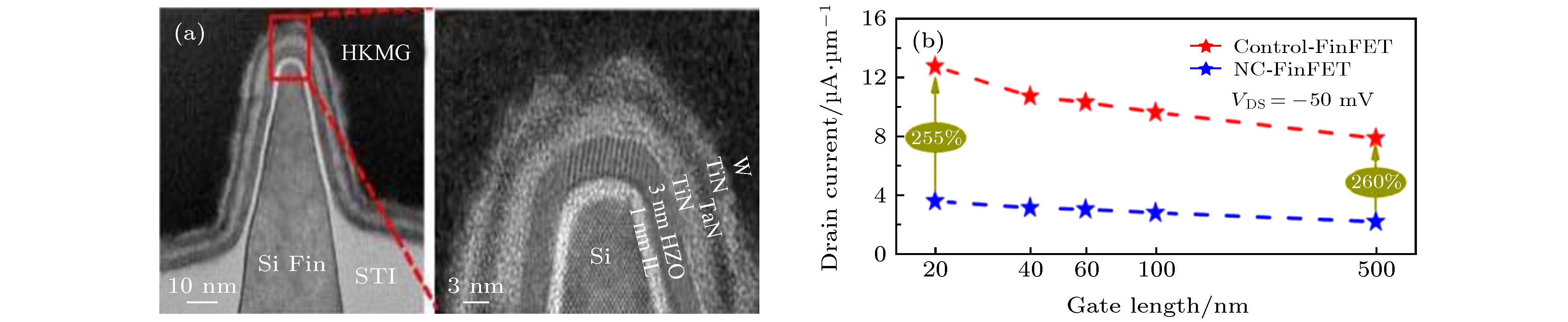

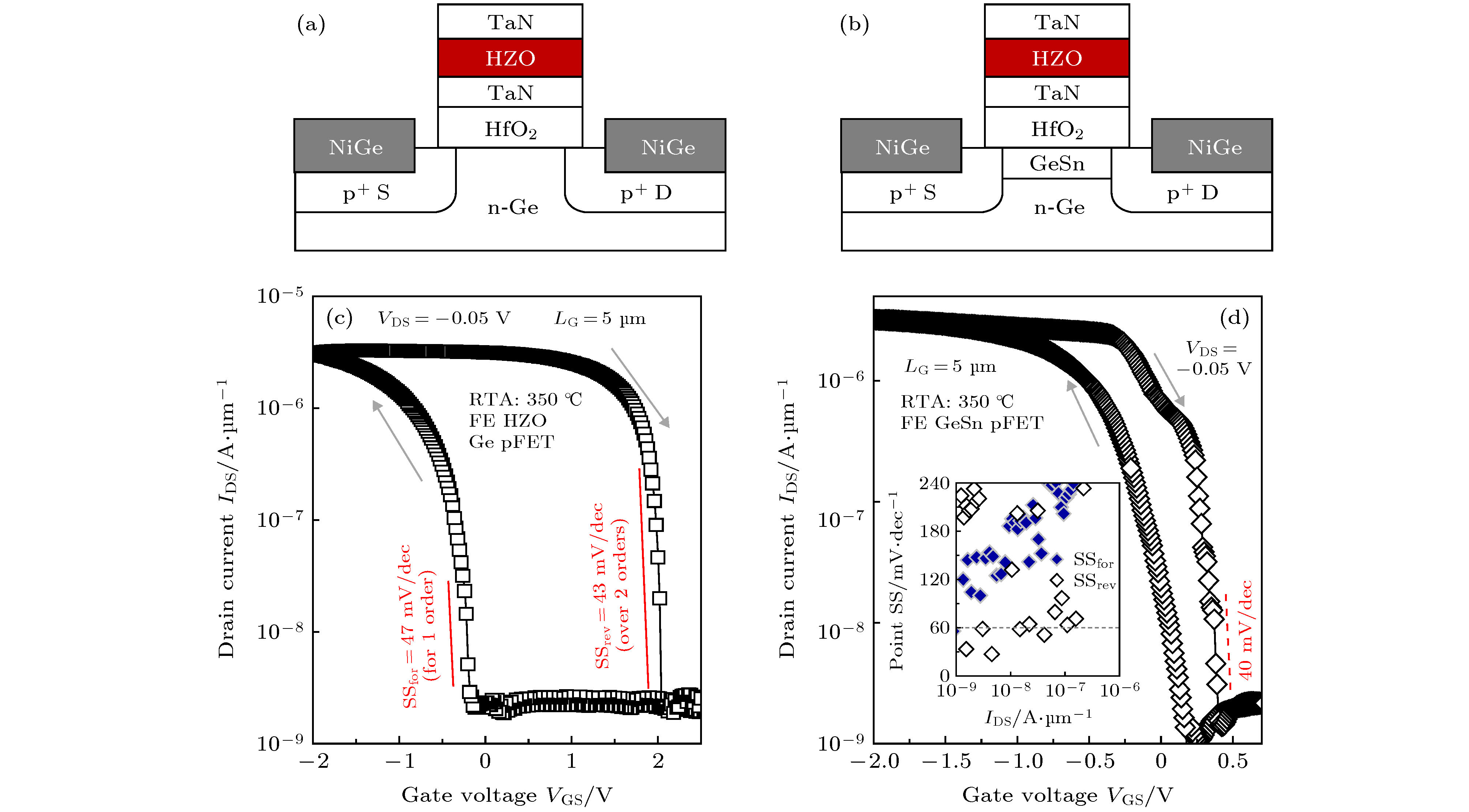
图 21 Ge基- HZO NCP型晶体管[129] (a) Ge沟道器件结构示意图; (b) Ge-Sn沟道器件结构示意图; (c) Ge沟道器件转移特性曲线; (d) Ge-Sn沟道器件转移特性曲线
Fig. 21. Germanium based HZO NC-pFET[129]: (a) Schematic diagram of the device with Ge channel; (b) schematic diagram of the device with Ge-Sn channel; (c) transfer characteristic curve of the device with Ge channel; (d) transfer characteristic curve of the device with Ge-Sn channel.

图 22 锗纳米线Fe-NCFETs[135] (a) 栅压扫描范围为 ±5 V时在不同扫描时间下的转移特性曲线; (b) 栅压扫描范围为 ±5 V时的回滞电压与扫描时间关系曲线; (c) 不同栅压扫描范围下的ID, Max与扫描时间关系曲线
Fig. 22. Germanium nanowire NC-pFET[135]: (a) The transfer characteristic curve at different sweep times for ±5 V sweep range; (b) hysteresis versus sweep time for ±5 V sweep range; (c) maximum drain current versus sweep time for different sweep ranges.

图 23 In0.53Ga0.47As沟道Fe-NCFETs (a) 平面型器件的结构示意图[136]; (b) Fin结构器件的结构示意图平[137]; (c) 平面型器件的转移特性曲线[136]; (d) Fin结构器件的转移特性曲线[137]
Fig. 23. In0.53Ga0.47As channel Fe-NCFETs: (a) Schematic diagram[136] and (c) transfer characteristic curve of planar device[136]; (b) schematic diagram[137] and (d) transfer characteristic curve of Fin device[137].


图 27 石墨烯- HfxAlyO2晶体管[154] (a) 在石墨烯/二氧化硅衬底上沉积的HfxAlyO2薄膜; (b) HfxAlyO2的相对介电常数; (c) 不同Al组分下HfxAlyO2三个相的能量差; (d) 转移特性曲线(9.5% Al)
Fig. 27. Graphene-HfxAlyO2 transistor[154]: (a) HfxAlyo2 films deposited on graphene/SiO2 substrates; (b) relative dielectric constant of HfxAlyO2; (c) energy difference among three phases in HfxAlyO2 with different Al concentrations; (d) transfer characteristic curve.
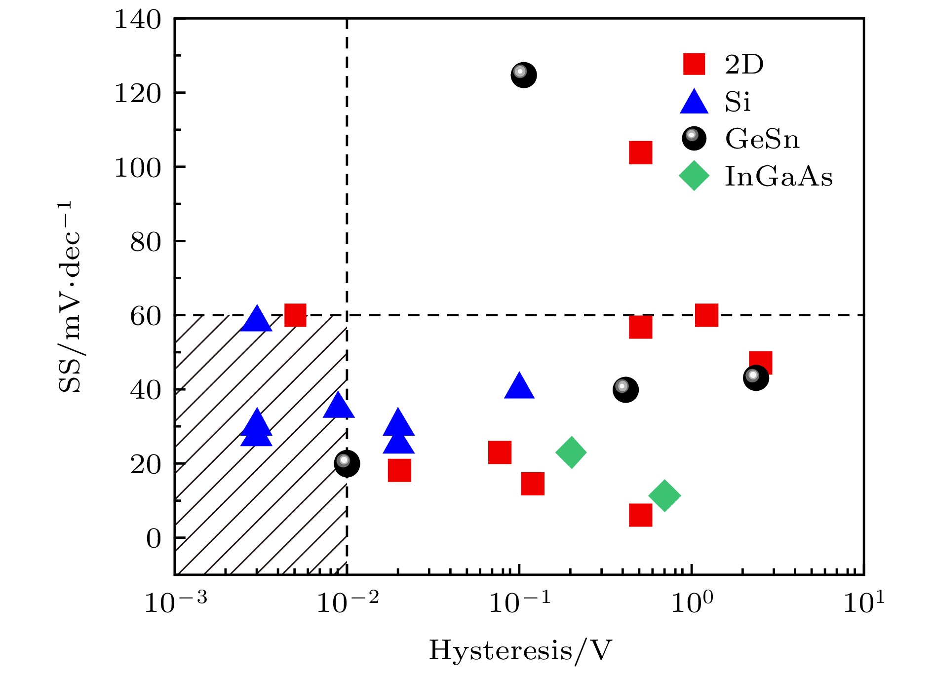
图 29 实验报道的Fe-NCFETs的SS与Hysteresis关系图 (2D[30,33,108,140,144,146-148,155], Si[25,116,118,119,121,123-126], GeSn[129,130,134,156], InGaAs[136,137])
Fig. 29. SS versus Hysteresis of the reported Fe-NCFETs (2D[30,33,108,140,144,146-148,155], Si[25,116,118,119,121,123-126], GeSn[129,130,134,156], InGaAs[136,137]).
表 1 实验报道的Fe-NCFETs的性能参数对比
Table 1. Performance comparison of the reported Fe-NCFETs.
MOS structure Channel materials Gate structure Ferroelectric materials tFE/nm SSmin/
(mV·dec–1)Hysteresis/V Orders
of IDSVD/V ION/IOFF Year Ref. Planar p-Si MFIS Hf0.65Zr0.35O2 30 5 — — –0.5 104 2014 [115] Planar n-Si MFIS HfAlO (Al: 6%) 10 Sub-25 0.02 4 0.2 108 2017 [116] Planar n-Si MFIS Hf0.75Zr0.25O2 10 40 Free 1 0.2 107 2018 [119] Planar n-Si MFIS Hf0.53Zr0.47O2 5 ~40 ~0.1 2 0.2 107 2019 [121] Planar n-Si MFIS HfAlO (Al: 4%) 10 Sub-30 0.02 4 0.2 108 2019 [118] FinFET n-Si MFIS Hf0.5Zr0.5O2 4 Sub-30 0.003 2 0.05 107 2018 [25] FinFET n-Si MFMIS Hf0.42Zr0.58O2 5 58 0.003 1 0.1 105 2015 [123] FinFET n-Si MFIS Hf0.5Zr0.5O2 5 Sub-60 Free — 0.1 107 2019 [125] FinFET p-Si MFMIS Hf0.42Zr0.58O2 3 34.5 0.009 2 –0.05 104 2019 [124] FinFET n-Si MFIS Hf0.5Zr0.5O2 5 Sub-60 Free — 0.1 107 2019 [125] GAA poly n-Si MFIS Hf0.5Zr0.5O2 10 26.84 0.003 4 0.1 108 2019 [126] Planar p-Ge MFMIS Hf0.5Zr0.5O2 6.5 43 2.34 1 –0.05 103 2016 [129] Planar p-GeSn MFMIS Hf0.5Zr0.5O2 6.5 40 0.41 2 –0.05 103 2016 [129] Planar p-GeSn MFMIS Hf0.5Zr0.5O2 6 Sub-20 < 0.01 2 –0.05 104 2017 [130] Planar p-Ge MFMIS Hf0.5Zr0.5O2 4.5 ~87.5 Free — –0.05 103 2019 [156] Planar p-Ge MFIS Hf0.67Zr0.33O2 7 ~125 ~0.105 — –0.5 104 2019 [134] Planar n-InGaAs MFIS Hf0.5Zr0.5O2 8 23 ~0.2 3 0.05 105 2018 [136] FinFET n-InGaAs MFIS Hf0.5Zr0.5O2 5 23 0.2 1 0.05 103 2019 [137] GAA nanotube MFMIS HfAlO(Al: 7%) 10 ~45 — — 0.05 104 2018 [138] 2D-FET MoS2 MFMIS Hf1-xZrxO2 15 Sub-60 1.2 3 0.5 105 2017 [146] 2D-FET MoS2 MFMIS Hf0.5Zr0.5O2 15 6.07 0.5 4 0.5 105 2017 [33] 2D-FET MoS2 MFMIS HfAlO(Al:7.3%) 10 57 0.5 4 0.5 105 2017 [108] 2D-FET MoS2 MFMIS HfZrOx 15 47 2.5 1 0.1 106 2018 [30] 2D-FET MoS2 MFIS Hf0.5Zr0.5O2 20 Sub-60 < 0.005 4 0.5 106 2018 [147] 2D-FET MoS2 MFIS Hf0.5Zr0.5O2 20 23 0.077 6 0.1 109 2017 [144] 2D-FET WSe2 MFMIS Hf0.5Zr0.5O2 20 14.4 0.12 2 –0.1 105 2018 [140] 2D-FET WSe2 MFIS Hf0.5Zr0.5O2 10 18.2 0.02 4 –0.1 104 2018 [148] 2D-FET Graphene MFS HfAlO(Al:9.5%) 5 — — — 0.1 2.75 2016 [154] 2D-FET BP MFMIS Hf0.5Zr0.5O2 20 104 0.5 — 0.1 102 2019 [155]  下载: 导出CSV
-
[1] Moore G E 1965 Electronics 38 114
[2] Mori K, Duong A, Richardson W F J 2002 IEEE T. Electron Dev. 49 61
Google Scholar
[3] Fitzgerald E 2006 US Patent 11 412 262
[4] Chaudhry A, Kumar M J 2004 IEEE T. Device Ma. Re. 4 99
Google Scholar
[5] Tsutsui G, Saitoh M, Hiramoto T 2005 IEEE Electr. Device L. 26 836
Google Scholar
[6] Auth C, Allen C, Blattner A, Bergstrom D, Brazier M, Bost M, Buehler M, Chikarmane V, Ghani T, Glassman T 2012 Symposium on VLSI Technology Honolulu, HI, USA, June 12–14, 2012 p131
[7] Bae G, Bae D-I, Kang M, Hwang S, Kim S, Seo B, Kwon T, Lee T, Moon C, Choi Y 2019 IEEE International Electron Devices Meeting San Francisco, CA, USA, December 1–5, 2018 p28.7.1
[8] International Roadmap for Devices and Systems 2017 Edition Reports. https://irds.ieee.org/roadmap-2017 [2020-1-11].
[9] Zhirnov V V, Cavin R K 2008 Nat. Nanotechnol. 3 77
Google Scholar
[10] Woo Young C, Byung-Gook P, Jong Duk L, Tsu-Jae King L 2007 IEEE Electr. Device L. 28 743
Google Scholar
[11] Seabaugh A C, Zhang Q 2010 Proc. IEEE 98 2095
Google Scholar
[12] Ionescu A M, Riel H 2011 Nature 479 329
Google Scholar
[13] Mori T, Morita Y, Miyata N, Migita S, Fukuda K, Mizubayashi W, Masahara M, Yasuda T, Ota H 2015 Appl. Phys. Lett. 106 083501
Google Scholar
[14] Gopalakrishnan K, Griffin P B, Plummer J D 2003 Digest. International Electron Devices Meeting San Francisco, CA, USA, December 8–11, 2002 p289
[15] Kam H, Lee D T, Howe R T, King T J 2006 IEEE International Electron Devices Meeting, 2005. IEDM Technical Digest. Washington, DC, USA, December 5–5, 2005 p463
[16] Lefter M, Enachescu M, Voicu G R, Cotofana S D 2014 Proceedings of the 2014 IEEE/ACM International Symposium on Nanoscale Architectures Paris, France, July 15–17, 2014 p151
[17] Enachescu M, Lefter M, Voicu G R, Cotofana S D 2018 IEEE Trans. Emerg. Top. Comput. 6 184
Google Scholar
[18] Luong G V, Narimani K, Tiedemann A T, Bernardy P, Trellenkamp S, Zhao Q T, Mantl S 2016 IEEE Electr. Device L. 37 950
Google Scholar
[19] Kumar M J, Maheedhar M, Varma P P 2015 IEEE T. Electron Dev. 62 4345
Google Scholar
[20] Enachescu M, Voicu G R, Cotofana S D 2012 IEEE International Symposium on Circuits and Systems Seoul, South Korea, May 23–25, 2012 p2561
[21] Wei S, Zhang G, Liu J, Huang H, Geng L, Shao Z, Yang C F 2017 International Conference on Applied System Innovation (ICASI) Sapporo, Japan, May 13–17, 2017 p1293
[22] Colinge J P, Lee C W, Afzalian A, Akhavan N D, Yan R, Ferain I, Razavi P, O'Neill B, Blake A, White M, Kelleher A M, McCarthy B, Murphy R 2010 Nat. Nanotechnol. 5 225
Google Scholar
[23] Wang H, Han W, Li X, Zhang Y, Yang F 2014 J. Appl. Phys. 116 124505
Google Scholar
[24] Salahuddin S, Datta S J 2008 Nano Lett. 8 405
Google Scholar
[25] Zhou H, Kwon D, Sachid A B, Liao Y, Chatterjee K, Tan A J, Yadav A K, Hu C, Salahuddin S 2018 IEEE Symposium on VLSI Technology Honolulu, HI, USA, June 18–22, 2018 p53
[26] Kobayashi M 2018 Appl. Phys. Express 11 110101
Google Scholar
[27] Tan A J, Zhu Z, Choe H S, Hu C, Salahuddin S, Yoon A 2019 International Symposium on VLSI Technology, Systems and Application Hsinchu, Taiwan, China, April 22–25, 2019 p1
[28] Das S, Appenzeller J 2011 Nano Lett. 11 4003
Google Scholar
[29] Wang X, Yu P, Lei Z, Zhu C, Cao X, Liu F, You L, Zeng Q, Deng Y, Zhu C, Zhou J, Fu Q, Wang J, Huang Y, Liu Z 2019 Nat. Commun. 10 3037
Google Scholar
[30] Xu J, Jiang S Y, Zhang M, Zhu H, Chen L, Sun Q Q, Zhang D W 2018 Appl. Phys. Lett. 112 103104
Google Scholar
[31] Rusu A, Salvatore G A, Jiménez D, Ionescu A M 2010 International Electron Devices Meeting San Francisco, CA, USA, December 6–8, 2010 p16.3.1
[32] Hu C, Salahuddin S, Lin C I, Khan A 2015 73rd Annual Device Research Conference Columbus, OH, USA, June 21–24, 2015 p39
[33] McGuire F A, Lin Y C, Price K, Rayner G B, Khandelwal S, Salahuddin S, Franklin A D 2017 Nano Lett. 17 4801
Google Scholar
[34] Pahwa G, Agarwal A, Chauhan Y S 2018 IEEE T. Electron Dev. 65 5130
Google Scholar
[35] Mehta H, Kaur H 2019 4th International Conference on Devices, Circuits and Systems Coimbatore, India, March 16–17, 2018 p164
[36] Mehta H, Kaur H 2018 IEEE T. Electron Dev. 65 2699
Google Scholar
[37] Shao Q, Wang X, Jiang W, Chen Y, Zhang X, Tu L, Lin T, Shen H, Meng X, Liu A, Wang J 2019 Appl. Phys. Lett. 115 162902
Google Scholar
[38] Fan C C, Tu C Y, Lin M H, Chang C Y, Cheng C H, Chen Y L, Liou G L, Liu C, Chou W C, Hsu H H 2018 IEEE International Reliability Physics Symposium Burlingame, CA, USA, March 11–15, 2018 pP-TX.8-1
[39] 钟维烈 1996 铁电体物理学 (北京: 科学出版社) 第1页
Zhong W L 1996 Ferroelectric Physics (Beijing: Science Press) p1 (in Chinese)
[40] Kholkin A L, Pertsev N A, Goltsev A V 2008 Piezoelectricity and Crystal Symmetry (Boston: Springer US) pp28–29
[41] Koh J H 2002 Ph. D. Dissertation (Stockholm: Royal Institute of Technology)
[42] Wersing W, Bruchhaus R 2000 Pyroelectric Devices and Applications (Cambridge: Academic Press) p143
[43] Sawaguchi E, Akishige Y, Kobayashi M 1985 J. Phys. Soc. Jpn. 54 480
Google Scholar
[44] Lu S W, Lee B I, Wang Z L, Samuels W D 2000 J. Cryst. Growth 219 269
Google Scholar
[45] Smith M B, Page K, Siegrist T, Redmond P L, Walter E C, Seshadri R, Brus L E, Steigerwald M L 2008 J. Am. Chem. Soc. 130 6955
Google Scholar
[46] Valasek J 1921 Phys. Rev. 17 475
Google Scholar
[47] Ploss B, Ploss B, Shin F G, Chan H L, Choy C L 2000 IEEE Trns. Dielectr. Electr. Insul. 7 517
Google Scholar
[48] Nguyen C A, Mhaisalkar S G, Ma J, Lee P S 2008 Org. Electron. 9 1087
Google Scholar
[49] Kang S J, Park Y J, Bae I, Kim K J, Kim H C, Bauer S, Thomas E L, Park C 2009 Adv. Funct. Mater. 19 2812
Google Scholar
[50] Jo J, Choi W Y, Park J D, Shim J W, Yu H Y, Shin C 2015 Nano Lett. 15 4553
Google Scholar
[51] Zhang W, Xiong R G 2012 Chem. Rev. 112 1163
Google Scholar
[52] Liu Y L, Ge J Z, Wang Z X, Xiong R G 2019 Inorg. Chem. Front. 7 128
Google Scholar
[53] Ikeda T, Sasaki T, Ichimura K 1993 Nature 361 428
Google Scholar
[54] Zhang H, Chen Y, Ding S, Wang J, Bao W, Zhang D W, Zhou P 2018 Nanotechnology 29 244004
Google Scholar
[55] Beresnev L A, Chigrinov V G, Dergachev D I, Poshidaev E P, Fünfschilling J, Schadt M 1989 Liq. Cryst. 5 1171
Google Scholar
[56] Ye H Y, Tang Y Y, Li P F, Liao W Q, Gao J X, Hua X N, Cai H, Shi P P, You Y M, Xiong R G J S 2018 Science 361 151
Google Scholar
[57] Li P F, Liao W Q, Tang Y Y, Qiao W, Zhao D, Ai Y, Yao Y F, Xiong R G 2019 Proc. Natl. Acad. Sci. U S.A 116 5878
Google Scholar
[58] Li L, Wu M 2017 ACS Nano 11 6382
Google Scholar
[59] Ding W, Zhu J, Wang Z, Gao Y, Xiao D, Gu Y, Zhang Z, Zhu W 2017 Nat. Commun. 8 14956
Google Scholar
[60] Li Y, Gong M, Zeng H 2019 J. Semicond. 40 061002s
Google Scholar
[61] Liu F, You L, Seyler K L, Li X, Yu P, Lin J, Wang X, Zhou J, Wang H, He H, Pantelides S T, Zhou W, Sharma P, Xu X, Ajayan P M, Wang J, Liu Z 2016 Nat. Commun. 7 12357
Google Scholar
[62] Wu M, Jena P 2018 Wiley Interdiscip. Rev.-Comput. Mol. Sci. 8 1365
Google Scholar
[63] Böscke T S, Müller J, Bräuhaus D, Schröder U, Böttger U 2011 Appl. Phys. Lett. 99 102903
Google Scholar
[64] Mueller S, Mueller J, Singh A, Riedel S, Sundqvist J, Schroeder U, Mikolajick T 2012 Adv. Funct. Mater. 22 2412
Google Scholar
[65] Müller J, Schröder U, Böscke T S, Müller I, Böttger U, Wilde L, Sundqvist J, Lemberger M, Kücher P, Mikolajick T, Frey L 2011 J. Appl. Phys. 110 114113
Google Scholar
[66] Starschich S, Boettger U 2017 J. Mater. Chem. C 5 333
Google Scholar
[67] Schroeder U, Mueller S, Mueller J, Yurchuk E, Martin D, Adelmann C, Schloesser T, van Bentum R, Mikolajick T 2013 ECS J. Solid State Sci. Technol. 2 N69
Google Scholar
[68] Schroeder U, Yurchuk E, Müller J, Martin D, Schenk T, Polakowski P, Adelmann C, Popovici M I, Kalinin S V, Mikolajick T 2014 Jpn. J. Appl. Phys. 53 08LE02
Google Scholar
[69] Müller J, Böscke T S, Bräuhaus D, Schröder U, Böttger U, Sundqvist J, Kücher P, Mikolajick T, Frey L 2011 Appl. Phys. Lett. 99 112901
Google Scholar
[70] Müller J, Boscke T S, Schroder U, Mueller S, Brauhaus D, Bottger U, Frey L, Mikolajick T 2012 Nano Lett. 12 4318
Google Scholar
[71] Terki R, Bertrand G, Aourag H, Coddet C 2008 Mater. Lett. 62 1484
Google Scholar
[72] Íñiguez J, Zubko P, Luk’yanchuk I, Cano A 2019 Nat. Rev. Mater. 4 243
Google Scholar
[73] Sayeef S, Supriyo D 2008 Nano Letter 8 405
[74] Lu P S, Lin C C, Su P 2019 International Symposium on VLSI Technology, Systems and Application Hsinchu, Taiwan, China, April 22–25, 2019 p1
[75] Muller J, Boscke T S, Schroder U, Hoffmann R, Mikolajick T, Frey L 2012 IEEE Electr. Device L. 33 185
Google Scholar
[76] Pahwa G, Dutta T, Agarwal A, Chauhan Y S 2017 IEEE T. Electron Dev. 64 1366
Google Scholar
[77] Park B E, Lee G G 2010 J. Korean Phys. Soc. 56 1484
Google Scholar
[78] Sun J, Zheng X 2011 IEEE T. Electron Dev. 58 3559
Google Scholar
[79] Sun J, Zheng X J, Li W 2012 Curr. Appl. Phys. 12 760
Google Scholar
[80] Jang K, Kobayashi M, Hiramoto T 2018 Jpn. J. Appl. Phys. 57 114202
Google Scholar
[81] Li Y, Lian Y, Samudra G S 2015 Semicond. Sci. Technol. 30 045011
Google Scholar
[82] Sun J, Li Y, Cao L 2019 J. Comput. Electron. 18 527
Google Scholar
[83] Hoffmann M, Pesic M, Slesazeck S, Schroeder U, Mikolajick T 2018 Nanoscale 10 10891
Google Scholar
[84] Cheng C H, Fan C C, Tu C Y, Hsu H H, Chang C Y 2019 IEEE T. Electron Dev. 66 825
Google Scholar
[85] Wong J C, Salahuddin S 2019 Proc. IEEE 107 49
Google Scholar
[86] Luttinger J M, Tisza L 1946 Phys. Rev. 70 954
Google Scholar
[87] Slater J C 1950 Phys. Rev. 78 748
Google Scholar
[88] Islam Khan A, Bhowmik D, Yu P, Joo Kim S, Pan X, Ramesh R, Salahuddin S 2011 Appl. Phys. Lett. 99 113501
Google Scholar
[89] Rabe K M, Dawber M, Lichtensteiger C, Ahn C H, Triscone J-M 2007 Physics of Ferroelectrics: A Modern Perspective (Berlin, Heidelberg: Springer Berlin Heidelberg) pp1–30
[90] Gao W, Khan A, Marti X, Nelson C, Serrao C, Ravichandran J, Ramesh R, Salahuddin S 2014 Nano Lett. 14 5814
Google Scholar
[91] Alam M A, Si M, Ye P D 2019 Appl. Phys. Lett. 114 090401
Google Scholar
[92] Liu Z, Bhuiyan M, Ma T 2019 IEEE International Electron Devices Meeting San Francisco, CA, USA, December 1–5, 2018 p31.2.1
[93] Hoffmann M, Slesazeck S, Mikolajick T, Hwang C S 2019 Ferroelectricity in Doped Hafnium Oxide: Materials, Properties and Devices (Cambridge: Woodhead Publishing) p473
[94] Khan A I, Chatterjee K, Wang B, Drapcho S, You L, Serrao C, Bakaul S R, Ramesh R, Salahuddin S 2015 Nat. Mater. 14 182
Google Scholar
[95] Jang K, Ueyama N, Kobayashi M, Hiramoto T 2018 IEEE J. Electron Devices Soc. 6 346
Google Scholar
[96] Kim K D, Kim Y J, Park M H, Park H W, Kwon Y J, Lee Y B, Kim H J, Moon T, Lee Y H, Hyun S D, Kim B S, Hwang C S 2019 Adv. Funct. Mater. 29 1808228
Google Scholar
[97] Han Q, Aleksa P, Tromm T C U, Schubert J, Mantl S, Zhao Q T 2019 Solid-State Electron. 159 71
Google Scholar
[98] Catalan G, Jiménez D, Gruverman A 2015 Nat. Mater. 14 137
Google Scholar
[99] Chang S C, Avci U E, Nikonov D E, Manipatruni S, Young I A 2018 Phys. Rev. Appl. 9 014010
Google Scholar
[100] Landau L, Khalatnikov I 1954 Dokl. Akad. Nauk SSSR. 96 469
Google Scholar
[101] Hoffmann M, Khan A I, Serrao C, Lu Z, Salahuddin S, Pešić M, Slesazeck S, Schroeder U, Mikolajick T 2018 J. Appl. Phys. 123 184101
Google Scholar
[102] Merz W J 1954 Phys. Rev. 95 690
Google Scholar
[103] Chang S-C, Avci U E, Nikonov D E, Young I A 2017 IEEE J. Explor. Solid-State Comput. Devices Circuits 3 56
Google Scholar
[104] Jin C, Saraya T, Hiramoto T, Kobayashi M 2019 IEEE J. Electron Devices Soc. 7 368
Google Scholar
[105] Wang H, Yang M, Huang Q, Zhu K, Zhao Y, Liang Z, Chen C, Wang Z, Zhong Y, Zhang X 2019 IEEE International Electron Devices Meeting San Francisco, CA, USA, December 1–5, 2018 p31.1.1
[106] Orihara H, Hashimoto S, Ishibashi Y 1994 J. Phys. Soc. Jpn. 63 1031
Google Scholar
[107] Jo J, Shin C 2016 IEEE Electr. Device L. 37 245
Google Scholar
[108] Nourbakhsh A, Zubair A, Joglekar S, Dresselhaus M, Palacios T 2017 Nanoscale 9 6122
Google Scholar
[109] Saeidi A, Jazaeri F, Bellando F, Stolichnov I, Enz C C, Ionescu A M 2017 47th European Solid-State Device Research Conference Leuven, Belgium, September 11–14, 2017 p78
[110] Galatage R, Bentley S, Suvarna P H, Krivokapic Z 2018 US Patent 10 141 414 B1
[111] Khan A I, Yeung C W, Hu C, Salahuddin S 2012 International Electron Devices Meeting Washington, DC, USA, December 5–7, 2011 p11.3.1
[112] Agarwal H, Kushwaha P, Lin Y K, Kao M Y, Liao Y H, Dasgupta A, Salahuddin S, Hu C 2019 IEEE Electr. Device L. 40 463
Google Scholar
[113] Si M, Su C J, Jiang C, Conrad N J, Zhou H, Maize K D, Qiu G, Wu C T, Shakouri A, Alam M A, Ye P D 2018 Nat. Nanotechnol. 13 24
Google Scholar
[114] Bohr M T, Young I A 2017 IEEE Micro 37 20
[115] Cheng C H, Chin A 2014 IEEE Electr.Device L. 35 274
Google Scholar
[116] Fan CC, Cheng CH, Chen YR, Liu C, Chang CY 2018 IEEE International Electron Devices Meeting San Francisco, CA, USA, December 2–6, 2017 p23.2.1
[117] Chiu YC, Cheng CH, Chang C-, Tang YT, Chen MC 2016 IEEE Symposium on VLSI Technology Honolulu, HI, USA, June 14–16, 2016 p1
[118] Cheng CH, Fan CC, Hsu HH, Wang SA, Chang CY 2019 Phys. Status Solidi-Rapid Res. Lett. 13 1800493
Google Scholar
[119] Cheng C H, Lin M H, Chen H Y, Fan C C, Liu C, Hsu H H, Chang C Y 2018 Phys. Status Solidi-Rapid Res. Lett. 13 1800573
Google Scholar
[120] Zeng B, Xiao W, Liao J, Liu H, Liao M, Peng Q, Zheng S, Zhou Y 2018 IEEE Electr. Device L. 39 1508
Google Scholar
[121] Chen K T, Liao C Y, Chen H Y, Lo C, Siang G Y, Lin Y Y, Tseng Y J, Chang C, Chueh C Y, Yang Y J, Liao M H, Li K S, Chang S T, Lee M H 2019 Microelectron. Eng. 215 110991
Google Scholar
[122] Xiao W, Liu C, Peng Y, Zheng S, Feng Q, Zhang C, Zhang J, Hao Y, Liao M, Zhou Y 2019 IEEE Electr. Device L. 40 714
Google Scholar
[123] Li K S, Chen P G, Lai T Y, Lin C H, Cheng C C, Chen C C, Wei Y J, Hou Y F, Liao M H, Lee M H 2016 IEEE International Electron Devices Meeting Washington, DC, USA, December 7–9, 2015 p22.6.1
[124] Zhang Z, Xu G, Zhang Q, Hou Z, Li J, Kong Z, Zhang Y, Xiang J, Xu Q, Wu Z, Zhu H, Yin H, Wang W, Ye T 2019 IEEE Electr. Device L. 40 367
Google Scholar
[125] Chen P J, Tsai M J, Hou F J, Wu Y C 2019 Silicon Nanoelectronics Workshop Kyoto, Japan, June 9–10, 2019 p1
[126] Lee S Y, Chen H W, Shen C H, Kuo P Y, Chung C C, Huang Y E, Chen H Y, Chao T S 2019 IEEE Electr. Device L. 40 1708
Google Scholar
[127] Bansal A K, Kumar M, Gupta C, Hook T B, Dixit A 2018 IEEE T. Electron Dev. 65 3548
Google Scholar
[128] Song Y, Zhou H, Xu Q, Luo J, Yin H, Yan J, Zhong H 2011 J. Electron. Mater. 40 1584
Google Scholar
[129] Zhou J, Han G, Li Q, Peng Y, Lu X, Zhang C, Zhang J, Sun QQ, Zhang D W, Hao Y 2017 IEEE International Electron Devices Meeting San Francisco, CA, USA, December 3–7, 2016 p12.2.1
[130] Zhou J, Han G, Peng Y, Liu Y, Zhang J, Sun Q Q, Zhang D W, Hao Y 2017 IEEE Electr. Device L. 38 1157
Google Scholar
[131] Li J, Zhou J, Han G, Liu Y, Peng Y, Zhang J, Sun Q Q, Zhang D W, Hao Y 2017 IEEE Electr. Device L. 38 1500
Google Scholar
[132] Zhou J, Han G, Li J, Liu Y, Peng Y, Zhang J, Sun Q Q, Zhang D W, Hao Y 2018 IEEE Electr.Device L. 39 622
Google Scholar
[133] Zhou J, Han G, Li J, Liu Y, Peng Y, Zhang J, Sun Q Q, Zhang D W, Hao Y 2018 IEEE Electr. Device L. 39 618
Google Scholar
[134] Peng Y, Liu Y, Han G, Zhang J, Hao Y 2019 Nanoscale Res. Lett. 14 125
Google Scholar
[135] Alghamdi S, Chung W, Si M, Peide D Y 2018 76th Device Research Conference Santa Barbara, CA, USA, June 24–27, 2018 p1
[136] Luc Q, Fan-Chiang C, Huynh S, Huang P, Do H, Ha M, Jin Y, Nguyen T, Zhang K, Wang H 2018 IEEE Symposium on VLSI Technology Honolulu, HI, USA, June 18–22, 2018 p47
[137] Chang E Y, Luc Q H, Tran N A, Lin Y C 2019 ECS Trans. 92 3
Google Scholar
[138] Srimani T, Hills G, Bishop M D, Radhakrishna U, Zubair A, Park R S, Stein Y, Palacios T, Antoniadis D, Shulaker M M 2018 IEEE Electr. Device L. 39 304
Google Scholar
[139] Tu L, Wang X, Wang J, Meng X, Chu J 2018 Adv. Electron. Mater. 4 1800231
Google Scholar
[140] Si M, Jiang C, Chung W, Du Y, Alam M A, Ye P D 2018 Nano Lett. 18 3682
Google Scholar
[141] Lee Y T, Kwon H, Kim J S, Kim H H, Lee Y J, Lim J A, Song YW, Yi Y, Choi WK, Hwang D K 2015 ACS Nano 9 10394
Google Scholar
[142] Heidler J, Yang S, Feng X, Müllen K, Asadi K 2018 Solid-State Electron. 144 90
Google Scholar
[143] Choi H, Shin C 2019 Phys. Status Solidi A 216 1900177
Google Scholar
[144] Yu Z, Wang H, Li W, Xu S, Song X, Wang S, Wang P, Zhou P, Shi Y, Chai Y 2018 IEEE International Electron Devices Meeting San Francisco, CA, USA, December 2-6, 2017 p23.6.1
[145] Yap W C, Jiang H, Liu J, Xia Q, Zhu W 2017 Appl. Phys. Lett. 111 013103
Google Scholar
[146] McGuire F A, Lin Y C, Rayner B, Franklin A D 2017 75th Annual Device Research Conference South Bend, IN, USA, June 25–28, 2017 p1
[147] Alghamdi S, Si M, Yang L, Peide D Y 2018 IEEE International Reliability Physics Symposium Burlingame, CA, USA, March 11–15, 2018 pP-TX.1-1
[148] Wang J, Guo X, Yu Z, Ma Z, Liu Y, Chan M, Zhu Y, Wang X, Chai Y 2019 IEEE International Electron Devices Meeting San Francisco, CA, USA, December 1–5, 2018 p22.3.1
[149] Si M, Peide D Y 2018 International Symposium on VLSI Technology, Systems and Application Hsinchu, Taiwan, April 16–19, 2018 p1
[150] Liu F, Zhou Y, Wang Y, Liu X, Wang J, Guo H 2016 NPJ Quantum Mater. 1 16004
Google Scholar
[151] Park N, Kang H, Park J, Lee Y, Yun Y, Lee J H, Lee S G, Lee Y H, Suh D 2015 ACS Nano 9 10729
Google Scholar
[152] Jie W, Hao J 2017 Nanoscale 10 328
[153] Lipatov A, Fursina A, Vo T H, Sharma P, Gruverman A, Sinitskii A 2017 Adv. Electron. Mater. 3 1700020
Google Scholar
[154] Lee Y, Jeon W, Cho Y, Lee M H, Jeong S J, Park J, Park S 2016 ACS Nano 10 6659
Google Scholar
[155] Tian H, Li Y-x, Li L, Wang X, Liang R, Yang Y, Ren T L 2019 IEEE T. Electron Dev. 66 1579
Google Scholar
[156] Li J, Liu Y, Han G, Zhou J, Hao Y 2019 Nanoscale Res. Lett. 14 171
Google Scholar
[157] Peng Y, Han G, Xiao W, Wu J, Liu Y, Zhang J, Hao Y 2019 Nanoscale Res. Lett. 14 115
Google Scholar
[158] Tokumitsu E 2020 Jpn. J. Appl. Phys. 59 SCCB06
Google Scholar
[159] Park J H, Jang G S, Kim H Y, Seok K H, Chae H J, Lee S K, Joo S K 2016 Sci. Rep. 6 24734
Google Scholar
[160] Lee M H, Fan S T, Tang C H, Chen P G, Chou Y C, Chen H H, Kuo J Y, Xie M J, Liu S N, Liao M H 2017 IEEE International Electron Devices Meeting San Francisco, CA, USA, December 3–7, 2016 p12.1.1
[161] Zhang X D, Han W H, Liu W, Zhao X S, Guo Y Y, Yang C, Chen J D, Yang F H 2019 Chin. Phys. B 28 127302
Google Scholar
[162] Guo Y Y, Han W H, Zhao X S, Dou Y M, Zhang X D, Wu X Y, Yang F H 2019 Chin. Phys. B 28 107303
Google Scholar
[163] Zhao X S, Han W H, Guo Y Y, Dou Y M, Yang F H 2018 Chin. Phys. B 27 097310
Google Scholar


 下载:
下载:


计量
- 文章访问数: 44198
- PDF下载量: 1932
- 被引次数: 0
