-
Aiming at three-dimensional (3D) sensing applications such as LiDAR, high power density five-junction cascaded vertical cavity surface emitting lasers (VCSELs) with 905 nm wavelength are designed and fabricated. The maximum power conversion efficiency is 55.2% for an individual VCSEL emitter with 8 μm oxide aperture. And the maximum slope efficiency of the device is 5.4 W/A, which is approximately 5 times that of traditional single-junction VCSEL with the same aperture. Under the condition of narrow pulse (pulse width 5.4 ns, duty cycle 0.019%) injection, the peak output power of 19-element array (20 μm oxidation aperture for each element) reaches 58.3 W, and the corresponding power density is as high as 1.62 kW/mm2. The devices with various apertures (8–20 μm) are characterized. The results show that the maximum slope efficiencies of all these devices are greater than 5.4 W/A and the maximum PCE is higher than 54%. These high-performance VCSEL devices can be used as ideal light sources for 3D sensing applications such as LiDAR.
-
Keywords:
- 905 nm vertical cavity surface emitting lasers /
- multi-junction cascade /
- high power density /
- 3-dimensional sensing
[1] Schwarz B 2010 Nat. Photonics 4 7
[2] Kirkpatrick K 2018 Commun. ACM 61 6
[3] Kim J S, Yun S J, Seol D J, Park H J, Kim Y S 2015 IEEE Sens. J. 15 12
[4] Warren M E 2019 IEEE Symposium on VLSI Circuits Kyoto, Japan, June 9–14, 2019 pC254–C255
[5] Seurin J F, Zhou D L, Xu G Y, Miglo A, Li D Z, Chen T, Guo B M, Ghosh C 2016 Proc. SPIE: Conference on Vertical-Cavity Surface-Emitting Lasers XX San Francisco, CA, February 17–18, 2016 p97660D
[6] Xie Y Y, Ni P N, Wang Q H, Kan Q, Briere G, Chen P P, Zhao Z Z, Delga A, Ren H R, Chen H D, Xu C, Genevet P 2020 Nat. Nanotechnol. 15 125
 Google Scholar
[7] Cheng C H, Shen C C, Kao H Y, et al. 2018 Opto-Electron. Adv. 1 3
[8] Chang-Hasnain C J 2019 IEEE 24th Microoptics Conference (MOC) Toyama, Japan, November 17–20, 2019 p18
[9] Larsson A 2011 IEEE J. Sel. Top. Quantum Electron. 17 6
[10] Liu A, Wolf P, Lott J A, et al. 2019 Photonics Res. 7 2
 Google Scholar
[11] Koyama F 2014 Opt. Rev. 21 6
[12] Miller M, Grabherr M, King R, et al. 2001 IEEE J. Sel. Top. Quantum Electron 7 2
[13] Knodl T, Straub A, Golling M, Michalzik R, Ebeling K J 2001 IEEE Photonics Technol. Lett. 13 9
[14] Müller M, Philippens M, Grönninger G, et al. 2007 Int. Soc. Opt. Photonics 2007 p6456
[15] Boucher J F, Vilokkinen V, Rainbow P 2009 Proc. SPIE Int. Soc. Opt. Eng. 2009 p74800K
[16] Kotaki Y, Uchiyama S, Iga K 1984 16 th (1984 International) Conference on Solid State Devices and Materials Kobe, Japan, August 30–September 1, 1984 p133
[17] Schmid W, Wiedenmann D, Grabherr M, Jager R, Michalzik R, Ebeling K J 1998 Electron. Lett. 34 6
 Google Scholar
[18] Knodl T, Golling M, Straub A, Ebeling K J 2001 Electron. Lett. 37 1
 Google Scholar
[19] Kim J K, Hall E, Nakagawa S, Huntington A, Coldren L A 2000 IEEE 17th International Semiconductor Laser Conf. 2000 p155
[20] Pan G, Xun M, Zhao Z, et al. 2021 IEEE Electron Device Lett. 42 9
[21] Xun M, Pan G, Zhao Z Z, et al. 2021 IEEE Trans. Electron Devices 68 6
-
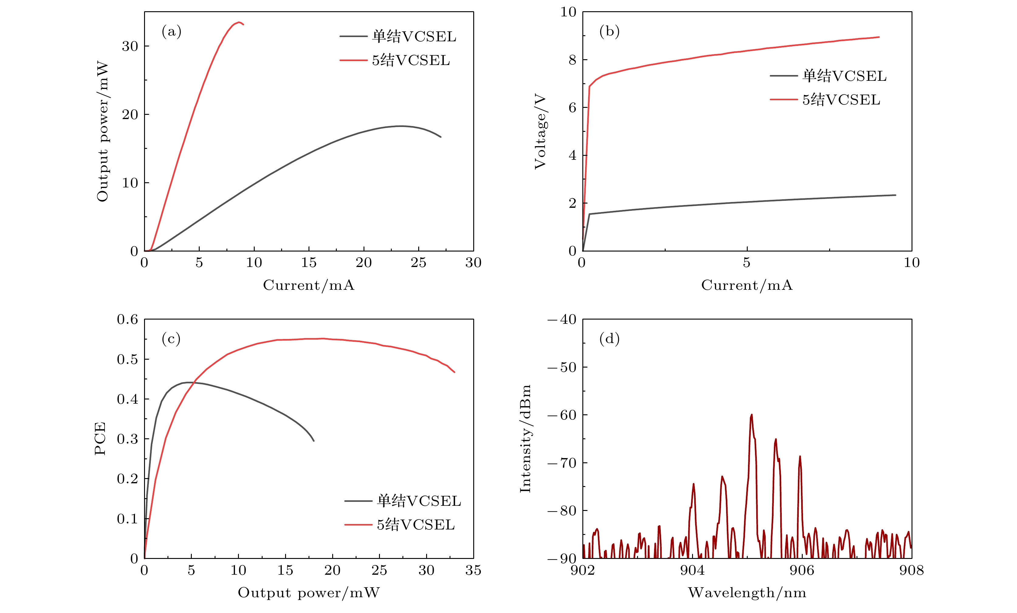
图 2 氧化孔径8 μm的5结VCSEL与单结VCSEL在室温CW条件下的测试结果 (a) L-I曲线; (b) V-I曲线; (c) PCE-L曲线; (d) 5结VCSEL在1 mA下的光谱
Figure 2. Measured results of 5-junction VCSEL and single junction VCSEL with 8 μm oxide aperture under CW condition at room temperature: (a) L-I curves; (b) V-I curves; (c) PCE-L curves; (d) spectrum of 5-junction VCSEL measured at 1 mA.
图 6 (a) 制备的19单元5结VCSEL阵列的俯视图和尺寸示意图; (b) 驱动板电压为25 V下阵列的光功率响应曲线; (c) 19单元阵列的峰值输出功率随驱动板电压的变化
Figure 6. (a) Structure and size diagram of the fabricated19-element 5-junction VCSEL array; (b) the optical power response curve of the array at driving circuit board voltage of 25 V; (c) peak output power of the array versus circuit board driving voltage.
-
[1] Schwarz B 2010 Nat. Photonics 4 7
[2] Kirkpatrick K 2018 Commun. ACM 61 6
[3] Kim J S, Yun S J, Seol D J, Park H J, Kim Y S 2015 IEEE Sens. J. 15 12
[4] Warren M E 2019 IEEE Symposium on VLSI Circuits Kyoto, Japan, June 9–14, 2019 pC254–C255
[5] Seurin J F, Zhou D L, Xu G Y, Miglo A, Li D Z, Chen T, Guo B M, Ghosh C 2016 Proc. SPIE: Conference on Vertical-Cavity Surface-Emitting Lasers XX San Francisco, CA, February 17–18, 2016 p97660D
[6] Xie Y Y, Ni P N, Wang Q H, Kan Q, Briere G, Chen P P, Zhao Z Z, Delga A, Ren H R, Chen H D, Xu C, Genevet P 2020 Nat. Nanotechnol. 15 125
 Google Scholar
[7] Cheng C H, Shen C C, Kao H Y, et al. 2018 Opto-Electron. Adv. 1 3
[8] Chang-Hasnain C J 2019 IEEE 24th Microoptics Conference (MOC) Toyama, Japan, November 17–20, 2019 p18
[9] Larsson A 2011 IEEE J. Sel. Top. Quantum Electron. 17 6
[10] Liu A, Wolf P, Lott J A, et al. 2019 Photonics Res. 7 2
 Google Scholar
[11] Koyama F 2014 Opt. Rev. 21 6
[12] Miller M, Grabherr M, King R, et al. 2001 IEEE J. Sel. Top. Quantum Electron 7 2
[13] Knodl T, Straub A, Golling M, Michalzik R, Ebeling K J 2001 IEEE Photonics Technol. Lett. 13 9
[14] Müller M, Philippens M, Grönninger G, et al. 2007 Int. Soc. Opt. Photonics 2007 p6456
[15] Boucher J F, Vilokkinen V, Rainbow P 2009 Proc. SPIE Int. Soc. Opt. Eng. 2009 p74800K
[16] Kotaki Y, Uchiyama S, Iga K 1984 16 th (1984 International) Conference on Solid State Devices and Materials Kobe, Japan, August 30–September 1, 1984 p133
[17] Schmid W, Wiedenmann D, Grabherr M, Jager R, Michalzik R, Ebeling K J 1998 Electron. Lett. 34 6
 Google Scholar
[18] Knodl T, Golling M, Straub A, Ebeling K J 2001 Electron. Lett. 37 1
 Google Scholar
[19] Kim J K, Hall E, Nakagawa S, Huntington A, Coldren L A 2000 IEEE 17th International Semiconductor Laser Conf. 2000 p155
[20] Pan G, Xun M, Zhao Z, et al. 2021 IEEE Electron Device Lett. 42 9
[21] Xun M, Pan G, Zhao Z Z, et al. 2021 IEEE Trans. Electron Devices 68 6
Catalog
Metrics
- Abstract views: 9977
- PDF Downloads: 309
- Cited By: 0


 DownLoad:


