-
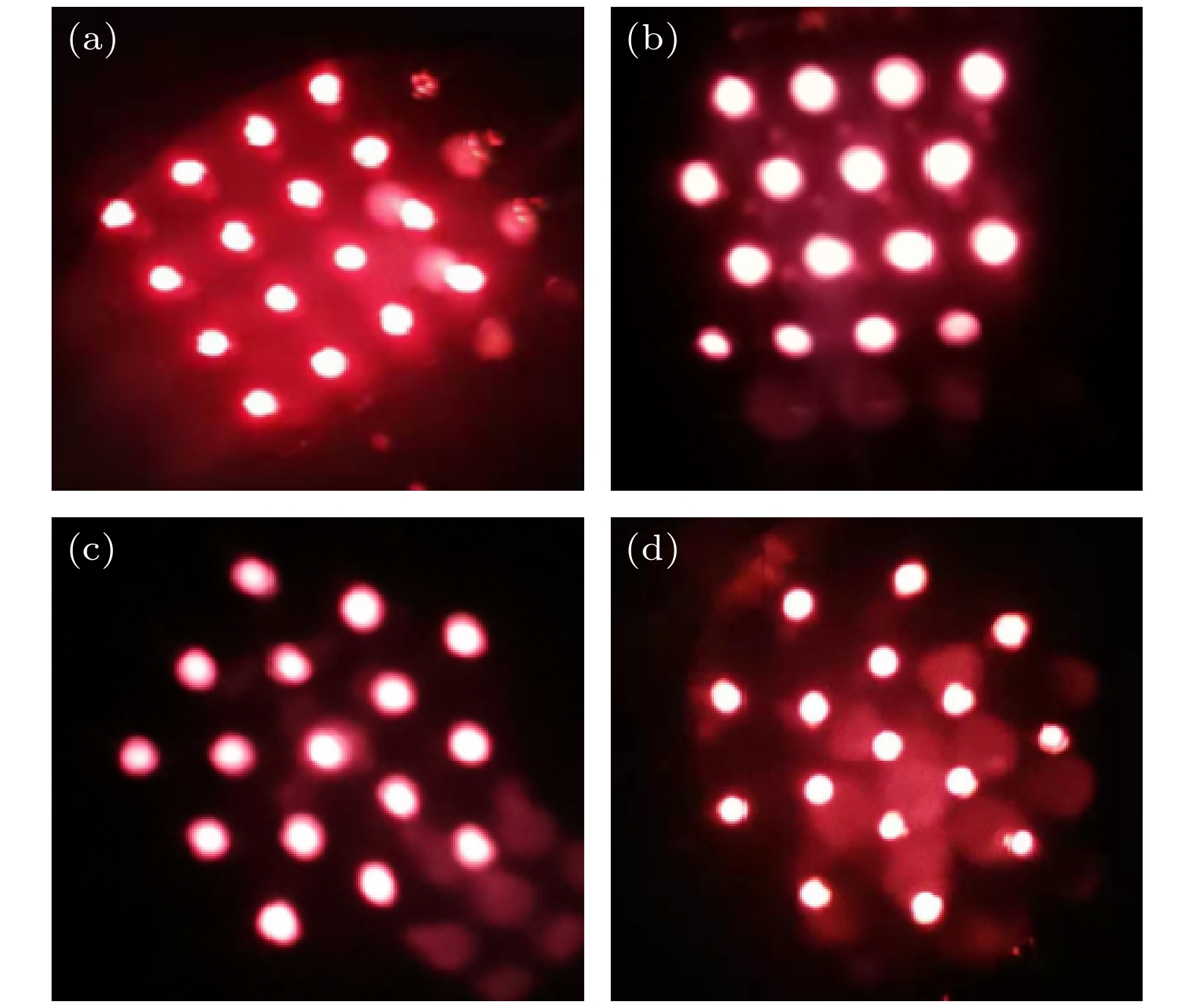
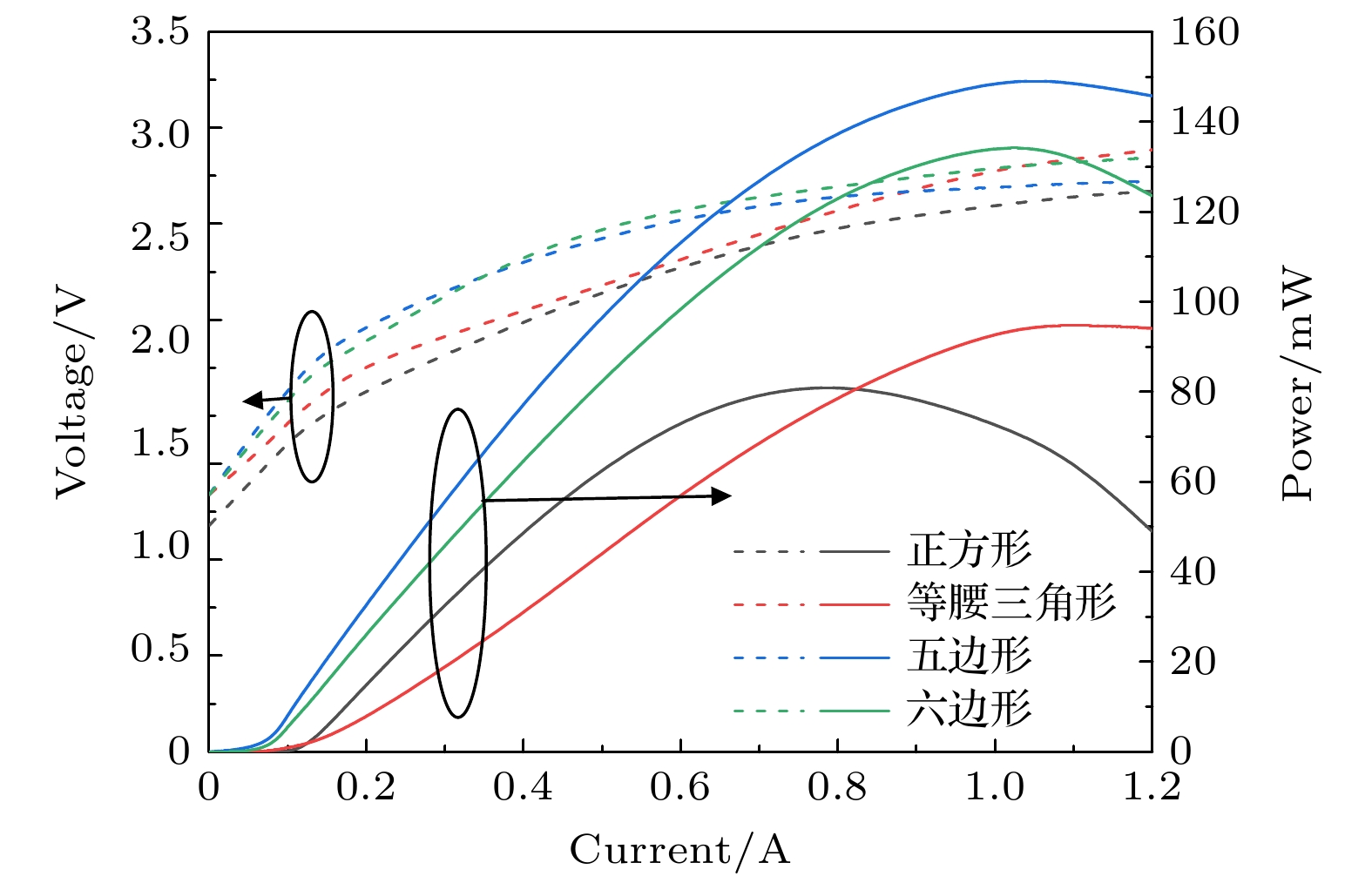
为了改善垂直腔面发射激光器(VCSEL )阵列的热特性, 提高器件的可靠性, 本文基于有限元模型, 研究了不同单元间距、排布方式对阵列器件的热串扰现象、热扩散性能的影响. 在理论分析的基础上, 制备了几种不同排布方式的VCSEL 阵列器件, 并对其进行测试分析. 结果显示, 相较于正方形排布方式, 新型排布方式器件具有更高的输出功率, 同时阈值电流也有所降低. 其中五边形排布方式的器件表现出最佳的性能, 其输出功率高达150 mW, 比正方形排布方式提高了约73%. 这表明通过调整阵列单元的间距、排列方式, 可以使各单元间的热串扰现象得到有效改善, 降低器件的热效应, 进而降低器件温度, 提高输出特性.Due to the excellent characteristics such as good beam quality, dynamic single-longitudinal mode, low power consumption, and good wavelength stability, especially easy-to-integrate high-density 2D area arrays, vertical-cavity surface-emitting laser (VCSEL) is widely used in optical identification, optical interconnection systems, optical data storage and other fields. In recent years, with the improvement of materials and process technology, VCSEL has played an increasingly important role in the fields of smartphone face recognition, drone obstacle avoidance, virtual reality/augmented reality (VR/AR), sweeping robots, home cameras, etc., and with the rapid development and application of 5G communication, VCSEL will become an indispensable main component. However, due to the introduction of distributed Bragg mirrors, the thermal effect of VCSEL is very serious, especially when VCSEL is integrated into an array device, current-induced self-heating of each individual array cell and the thermal coupling among array cells have become the major factors contributing to thermal rollover and hence restraining the optical output performance of the VCSEL arrays. Therefor it is of great significance to study the thermal characteristics of VCSELs, in order to solve the problem of thermal crosstalk between single-tube devices, and increase the life of the device. This paper analyzes the influence of cell spacing and arrangement on the thermal crosstalk phenomenon and thermal diffusion performance of VCSEL array device based on the finite element model. The simulation results show that the maximum temperature of the device decays exponentially with the increase of cell spacing, the thermal crosstalk phenomenon and thermal diffusion performance of VCSEL array devices are significantly improved. When the cell spacing is 120 μm, the influence between the cells is small, the thermal crosstalk phenomenon is significantly improved, and the heat dissipation effect is better. On this basis, four non-square VCSEL arrays with 16 cells are designed, and it can be seen that compared with the square arrangement, the isosceles triangle, pentagonal and hexagonal configurations have improved the thermal crosstalk phenomenon and thermal diffusion performance, and the overall temperature rise of the VCSEL array is significantly reduced. The thermal crosstalk phenomenon of the pentagonal arrangement is significantly improved, and the device temperature is 37.32 ℃, which is the best effect among several arrangement methods. According to the results of theoretical simulation, the VCSEL array devices with different arrangements are prepared and characterized on the same epitaxial wafer by the same process. From the P-I-V characteristic curves, it can be seen that the threshold currents of isosceles triangles, pentagons and hexagons are lower than those of the square arrangement, and the maximum output power is higher than that of the square arrangement, especially the maximum output power value of the pentagonal is 150 mW. The results show that the new arrangement can effectively improve the thermal crosstalk phenomenon between the cells, increase the output power of the device, and make the VCSEL array device have good optoelectronic and thermal characteristics.
-
Keywords:
- vertical cavity surface emitting laser /
- array /
- thermal crosstalk /
- layout method
[1] Soda H, Iga K, Kitahara C, Suematsu Y 1979 Jpn. J. Appl. Phys. 18 2329
 Google Scholar
[2] Iga K 2018 Jpn. J. Appl. Phys. 57 08PA01
 Google Scholar
[3] Inoue S, Nishimura S, Nakahama M, Matsutani A, Sakaguchi T, Koyama F 2018 Jpn. J. Appl. Phys. 57 040308
 Google Scholar
[4] Kuramoto M, Kobayashi S, Akagi T, Tazawa K, Tanaka K, Nakata K, Saito T 2019 Appl. Phys. Express 12 091004
 Google Scholar
[5] 高亮 2014 硕士学位论文 (长春: 长春理工大学)
Gao L 2014 M. S. Thesis (Changchun: Changchun University of Science and Technology
[6] 赵秦丰 2020 硕士学位论文 (西安: 中国科学院大学)
Zhao Q Y 2020 M. S. Thesis (Xi’an: University of Chinese Academy of Sciences
[7] 张秋波2020硕士学位论文 (长春: 长春理工大学)
Zhang Q B 2020 M. S. Thesis (Changchun: Changchun University of Science and Technology
[8] Nakwaski W, Osinski M 1991 IEEE J. Quantum Elect. 27 1391
 Google Scholar
[9] Chen G, Hadley M A, Smith J S 1994 J. Appl. Phys. 76 3261
 Google Scholar
[10] Choi J H, Wang L, Bi H, Chen R T 2006 IEEE J Sel. Top Quant. 12 1060
 Google Scholar
[11] Desgreys P, Karray M, Charlot J, Charlot, Herve Y 2002 Proceedings of the 2002 IEEE International Workshop on Behavioral Modeling and Simulation Santa Rosa, CA, USA, 2002 pp123–126
[12] Moench H, Dumoulin R, Gronenborn S, Gu X, Heusler G, Kolb J, Miller M, Pekarski P, Pollmann-Retsch J, Pruijmboom A, Stroesser M 2012 SPIE 8276 9
 Google Scholar
[13] Wang J, Savidis I, Friedman E G 2011 Microelectronics J. 42 820
 Google Scholar
[14] Zhong C Y, Zhang X, Liu D, Ning Y Q, Wang L J 2017 Chin. Phys. B 26 064204
 Google Scholar
[15] Zhong C, Zhang X, Hofmann W, Ning Y Q, Wang L J 2018 IEEE Photon. J. 10 1504608
 Google Scholar
[16] Pan G Z, Xie Y Y, Xu C, Wang Q H, Dong Y B, Deng J, Chen H D, Sun J 2019 IEEE Photonic Tech. L. 31 1647
 Google Scholar
[17] Gao Z H, Thompson B J, Ragunathan G, Johnson M T, Rout B, Choquette K D IEEE Photonic Tech. L. 28 513–515
[18] Amann M C, Hofmann W 2009 IEEE J Sel. Top Quant. 15 861
 Google Scholar
[19] Jin D Y, Yang S M, Zhang F, Wu L, Guan B L, Yang Y Q, Zhang W R 2022 IEEE Trans. Electron Devices 69 3761
 Google Scholar
[20] Liu Y Y, Huang Y W, Zhong C Y, Zhang X, Zhang J W, Hofmann W, Ning Y Q, Wang L J 2019 Optik 186 443
 Google Scholar
[21] Wang C, Li C, Dai J 2019 Opt. Quantum Electron 51 1
 Google Scholar
[22] Qin Y X, Li W, Liu S P, Ma X Y 2019 J. Appl. Phys. 126 193101
 Google Scholar
-
表 1 模拟中采用的外延片结构参数和热参数
Table 1. Structural and thermal parameters of epitaxial wafers used in simulation.
各层参数 材料 热导率 κ/
(W·(cm·K)–1)厚度/μm P-DBR层(对) Al0.9GaAs/
Al0.22GaAs0.5 3.479 有源层 Al0.3GaAs/
Al0.6GaAs0.185 0.2373 N-DBR层(对) Al0.9GaAs/
Al0.22GaAs0.499 5.6408 衬底层 GaAs 0.55 150 欧姆接触层(N) Au-Ge-Ni 0.44 0.2 In焊料层 In 0.82 3 Cu热沉 Cu 3.98 1000 -
[1] Soda H, Iga K, Kitahara C, Suematsu Y 1979 Jpn. J. Appl. Phys. 18 2329
 Google Scholar
[2] Iga K 2018 Jpn. J. Appl. Phys. 57 08PA01
 Google Scholar
[3] Inoue S, Nishimura S, Nakahama M, Matsutani A, Sakaguchi T, Koyama F 2018 Jpn. J. Appl. Phys. 57 040308
 Google Scholar
[4] Kuramoto M, Kobayashi S, Akagi T, Tazawa K, Tanaka K, Nakata K, Saito T 2019 Appl. Phys. Express 12 091004
 Google Scholar
[5] 高亮 2014 硕士学位论文 (长春: 长春理工大学)
Gao L 2014 M. S. Thesis (Changchun: Changchun University of Science and Technology
[6] 赵秦丰 2020 硕士学位论文 (西安: 中国科学院大学)
Zhao Q Y 2020 M. S. Thesis (Xi’an: University of Chinese Academy of Sciences
[7] 张秋波2020硕士学位论文 (长春: 长春理工大学)
Zhang Q B 2020 M. S. Thesis (Changchun: Changchun University of Science and Technology
[8] Nakwaski W, Osinski M 1991 IEEE J. Quantum Elect. 27 1391
 Google Scholar
[9] Chen G, Hadley M A, Smith J S 1994 J. Appl. Phys. 76 3261
 Google Scholar
[10] Choi J H, Wang L, Bi H, Chen R T 2006 IEEE J Sel. Top Quant. 12 1060
 Google Scholar
[11] Desgreys P, Karray M, Charlot J, Charlot, Herve Y 2002 Proceedings of the 2002 IEEE International Workshop on Behavioral Modeling and Simulation Santa Rosa, CA, USA, 2002 pp123–126
[12] Moench H, Dumoulin R, Gronenborn S, Gu X, Heusler G, Kolb J, Miller M, Pekarski P, Pollmann-Retsch J, Pruijmboom A, Stroesser M 2012 SPIE 8276 9
 Google Scholar
[13] Wang J, Savidis I, Friedman E G 2011 Microelectronics J. 42 820
 Google Scholar
[14] Zhong C Y, Zhang X, Liu D, Ning Y Q, Wang L J 2017 Chin. Phys. B 26 064204
 Google Scholar
[15] Zhong C, Zhang X, Hofmann W, Ning Y Q, Wang L J 2018 IEEE Photon. J. 10 1504608
 Google Scholar
[16] Pan G Z, Xie Y Y, Xu C, Wang Q H, Dong Y B, Deng J, Chen H D, Sun J 2019 IEEE Photonic Tech. L. 31 1647
 Google Scholar
[17] Gao Z H, Thompson B J, Ragunathan G, Johnson M T, Rout B, Choquette K D IEEE Photonic Tech. L. 28 513–515
[18] Amann M C, Hofmann W 2009 IEEE J Sel. Top Quant. 15 861
 Google Scholar
[19] Jin D Y, Yang S M, Zhang F, Wu L, Guan B L, Yang Y Q, Zhang W R 2022 IEEE Trans. Electron Devices 69 3761
 Google Scholar
[20] Liu Y Y, Huang Y W, Zhong C Y, Zhang X, Zhang J W, Hofmann W, Ning Y Q, Wang L J 2019 Optik 186 443
 Google Scholar
[21] Wang C, Li C, Dai J 2019 Opt. Quantum Electron 51 1
 Google Scholar
[22] Qin Y X, Li W, Liu S P, Ma X Y 2019 J. Appl. Phys. 126 193101
 Google Scholar
计量
- 文章访问数: 3585
- PDF下载量: 119
- 被引次数: 0


 下载:
下载:


