


-
Strained silicon technology employing strain-relaxed SiGe virtual substrates has become pivotal factor in advancing group IV semiconductor electronics, photonic devices, silicon-based quantum computing architectures, and neuromorphic devices. Although existing approaches using Si/SiGe superlattice buffers and compositionally graded SiGe layers can produce high-quality SiGe virtual substrates, defects including threading dislocations and crosshatch patterns still limit further performance enhancement. This study demonstrates a method of fabricating fully elastically relaxed SiGe nanomembranes that effectively suppresses the formation of both threading dislocations and crosshatch patterns. The fabrication process comprises three key steps: 1) epitaxially growing Si/SiGe/Si heterostructures on silicon-on-insulator substrates via molecular beam epitaxy (MBE), 2) fabricating periodic pore arrays by using photolithography and reactive ion etching, and 3) selectively wet etching and subsequently transferring nanomembranes to Si(001) substrates. Subsequently, a Si/SiGe heterostructure is grown on the SiGe nanomembranes via MBE. The full elastic relaxation state of the SiGe nanomembranes and the fully strained state of the Si quantum well in the epitaxial Si/SiGe heterostructures are verified using Raman spectroscopy. Surface root-mean-square roughness value is 0.323 nm for the SiGe nanomembrane transferred to the silicon substrate and 0.118 nm for the epitaxial Si/SiGe heterostructure, which are demonstrated through atomic force microscopy measurements. Through electron channel contrast imaging, it is demonstrated that the Si/SiGe heterostructures grown on SiGe nanomembranes have uniform surface contrast and no detectable threading dislocations. Comparatively, the silicon substrate region exhibits high-density threading dislocations accompanied by stacking faults. Cross-sectional transmission electron microscope analysis shows atomically sharp and defect-free interfaces. This research lays a critical foundation for developing high-mobility two-dimensional electron gas systems and high-performance quantum bits.
-
Keywords:
- molecular beam epitaxy /
- stress relaxation /
- SiGe /
- heterojunction
[1] Theis T N, Wong H S P 2017 Comput. Sci. Eng. 19 41
 Google Scholar
[2] Shalf J 2020 Philos. Trans. R. Soc. Math. Phys. Eng. Sci. 378 20190061
Google Scholar
[3] Thompson S E, Parthasarathy S 2006 Mater. Today 9 20
Google Scholar
[4] Arienzo M, Iyer S S, Meyerson B S, Patton G L, Stork J M C 1991 Appl. Surf. Sci. 48 377
Google Scholar
[5] Azevedo A M D, Lopes T J, Cardoso D D, Monterio S N, Silveira P C R, Figueiredo A B H D S 2024 Obs. Econ. Latinoam. 22 e8370
Google Scholar
[6] Cressler J D 1998 IEEE Trans. Microw. Theory Tech. 46 572
Google Scholar
[7] Harame D L, Koester S J, Freeman G, Cottrel P, Rim K, Dehlinger G, Ahlgren D, Dunn J S, Greenberg D, Joseph A, Anderson F, Rieh J S, Onge S A S T, Coolbaugh D, Ramachandran V, Cressler J D, Subbanna S 2004 Appl. Surf. Sci. 224 9
Google Scholar
[8] Soref R A 1993 Proc. IEEE 81 1687
Google Scholar
[9] Wang K L, Cha D, Liu J, Chen C 2007 Proc. IEEE 95 1866
Google Scholar
[10] 张结印, 高飞, 张建军 2021 70 217802
Google Scholar
Zhang J Y, Gao F, Zhang J J 2021 Acta Phys. Sin. 70 217802
Google Scholar
[11] Tai C T, Li J Y 2024 Mater. Quantum Technol. 4 012001
Google Scholar
[12] Connors E J, Nelson J, Edge L F, Nichol J M 2022 Nat. Commun. 13 940
Google Scholar
[13] Bian H, Goh Y Y, Liu Y, Ling H, Xie L, Liu X 2021 Adv. Mater. 33 2006469
Google Scholar
[14] Fitzgerald E A, Xie Y H, Green M L, Brasen D, Kortan A R, Michel J, Mii Y J, Weir B E 1991 Appl. Phys. Lett. 59 811
Google Scholar
[15] Hartmann J M, Gallas B, Zhang J, Harris J J, Joyce B A 1999 J. Appl. Phys. 86 845
Google Scholar
[16] Rahman M M, Matada H, Tambo T, Tatsuyama C 2001 Appl. Surf. Sci. 175 6
Google Scholar
[17] Nelson S F, Ismail K, Nocera J J, Fang F F, Mendez E E, Chu J O, Meyerson B S 1992 Appl. Phys. Lett. 61 64
Google Scholar
[18] 耿鑫, 张结印, 卢文龙, 明铭, 刘方泽, 符彬啸, 褚逸昕, 颜谋回, 王保传, 张新定, 郭国平, 张建军 2024 73 117302
Google Scholar
Geng X, Zhang J Y, Lu W L, Ming M, Liu F Z, Fu B X, Chu Y X, Yan M H, Wang B C, Zhang X D, Guo G P, Zhang J J 2024 Acta Phys. Sin. 73 117302
Google Scholar
[19] Xie Y H, Fitzgerald E A, Mii Y J, Monroe D, Thiel F A, Weir B E, Feldman L C 1991 MRS Proc. 220 413
Google Scholar
[20] Ismail K 1996 J. Vac. Sci. Technol. B Microelectron. Nanometer Struct. Process. Meas. Phenom. 14 2776
Google Scholar
[21] Monroe D, Xie Y H, Fitzgerald E A, Silverman P J, Watson G P 1993 J. Vac. Sci. Technol. B Microelectron. Nanometer Struct. Process. Meas. Phenom. 11 1731
Google Scholar
[22] Paskiewicz D M, Tanto B, Savage D E, Lagally M G 2011 ACS Nano 5 5814
Google Scholar
[23] Li Y S, Sookchoo P, Cui X, Mohr R, Savage D E, Foote R H, Jacobson R, Sánchez-Pérez J R, Paskiewicz D M, Wu X, Ward D R, Coppersmith S N, Eriksson M A, Lagally M G 2015 ACS Nano 9 4891
Google Scholar
[24] Schäffler F 1997 Semicond. Sci. Technol. 12 1515
Google Scholar
[25] Schmidt O G, Eberl K 2001 Nature 410 168
Google Scholar
[26] Wolf I D 1996 Semicond. Sci. Technol. 11 139
Google Scholar
[27] Pezzoli F, Bonera E, Grilli E, Guzzi M, Sanguinetti S, Chrastina D, Isella G, Von Känel H, Wintersberger E, Stangl J, Bauer G 2008 J. Appl. Phys. 103 093521
Google Scholar
[28] Nakashima S, Mitani T, Ninomiya M, Matsumoto K 2006 J. Appl. Phys. 99 053512
Google Scholar
[29] Wong L H, Wong C C, Liu J P, Sohn D K, Chan L, Hsia L C, Zang H, Ni Z H, Shen Z X 2005 Jpn. J. Appl. Phys. 44 7922
Google Scholar
[30] Loup V, Gabette L, Roure M C, Kachtouli R, Jourdan M, Besson P, Petitdidier S 2013 ECS Trans. 58 47
Google Scholar
[31] Shikida M, Sato K, Tokoro K, Uchikawa D 2000 Sens. Actuators Phys. 80 179
Google Scholar
-
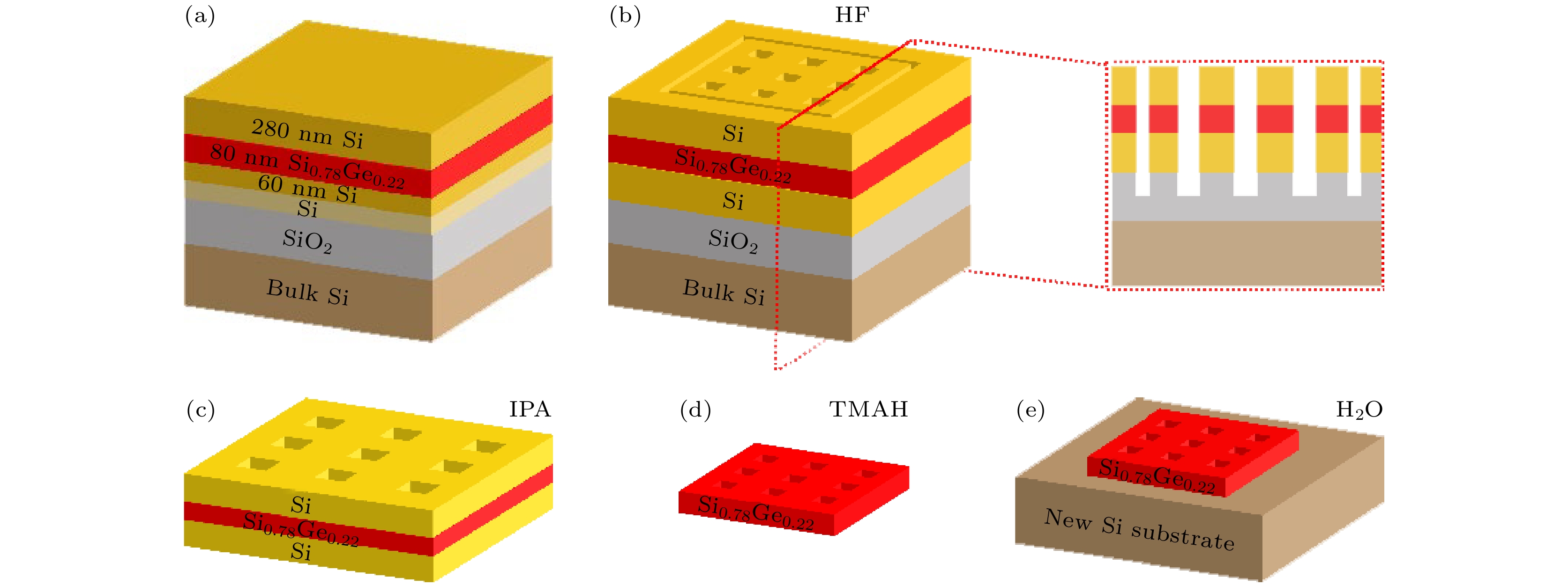
图 1 SiGe纳米薄膜的制备流程 (a) SOI衬底上外延生长60 nm Si, 80 nm Si0.78Ge0.22和280 nm Si; (b) 利用微纳加工技术制备周期孔洞阵列; (c) 在IPA溶液中将Si/SiGe/Si异质结和衬底进行分离; (d) 在TMAH溶液中选择性刻蚀掉上下Si层后的SiGe薄膜; (e) 在去离子水中将SiGe纳米薄膜转移到Si(001)衬底上
Figure 1. Fabrication processes of SiGe nanomembrane: (a) MBE epitaxial growth of 60 nm Si, 80 nm Si0.78Ge0.22, and 280 nm Si on an SOI substrate; (b) fabrication of a periodic hole array on such heterostructure; (c) separation of the Si/SiGe/Si heterostructure from the Si substrate in IPA solution; (d) selective etching of the Si layers over SiGe in TMAH solution; (e) transfer of the SiGe nanomembrane onto a Si (001) substrate in deionized water.
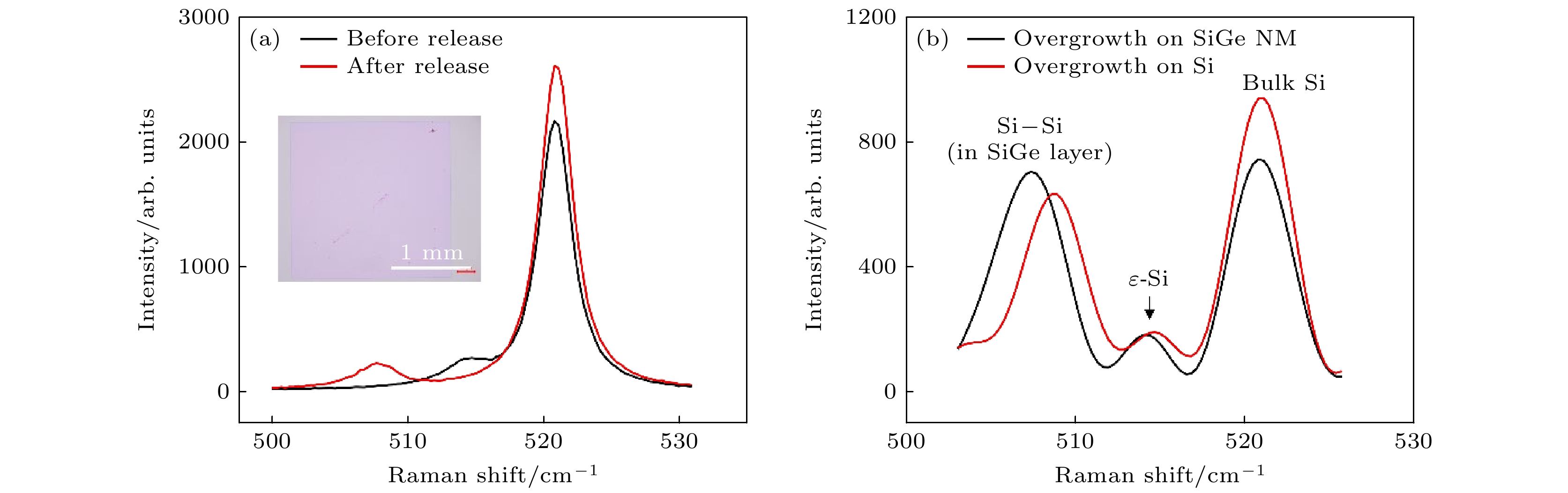
图 2 (a) Si0.78Ge0.22纳米薄膜在释放前(黑线)和释放后(红线)的拉曼光谱, 其中插图是Si0.78Ge0.22纳米膜转移到Si衬底后的光学显微镜图; (b) 在Si0.78Ge0.22纳米薄膜区域(黑线)和Si衬底区域(红线)生长Si/SiGe异质结后的拉曼光谱
Figure 2. (a) Raman spectra of Si0.78Ge0.22 nanomembrane before release (black line) and after release (red line), where the inset shows an optical microscope image of the Si0.78Ge0.22 nanomembrane transferred to a Si substrate; (b) Raman spectra after growing Si/SiGe heterostructure in the Si0.78Ge0.22 nanomembrane region (black line) and Si substrate region (red line).
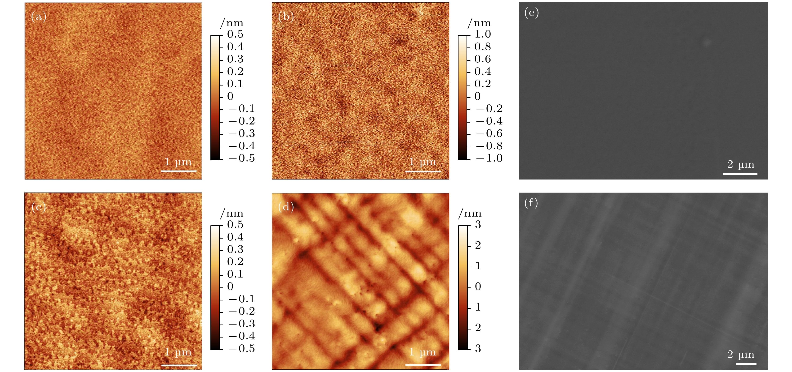
图 3 (a) SOI衬底上生长Si/SiGe/Si异质结后的表面AFM图; (b) Si0.78Ge0.22纳米薄膜转移到Si衬底后的表面AFM; (c) 转移Si0.78Ge0.22纳米薄膜区域上生长Si/SiGe异质结后的表面AFM图; (d) 在Si衬底区域直接生长Si/SiGe异质结后的表面AFM图; (e) 在Si0.78Ge0.22纳米薄膜区域生长Si/SiGe异质结后的表面ECCI图; (f)在Si衬底区域直接生长Si/SiGe异质结后的表面ECCI图
Figure 3. (a) AFM image of the surface after growing Si/SiGe/Si structure on an SOI substrate; (b) AFM image of the surface after transferring Si0.78Ge0.22 nanomembrane to a Si substrate; (c) AFM image of the surface after growing Si/SiGe heterostructure on the transferred Si0.78Ge0.22 nanomembrane region; (d) AFM image of the surface after directly growing Si/SiGe heterostructure on the Si region; (e) electron channel contrast imaging (ECCI) of the surface after growing Si/SiGe heterostructure on the Si0.78Ge0.22 nanomembrane region; (f) ECCI of the surface after directly growing Si/SiGe heterostructure on the Si substrate region.
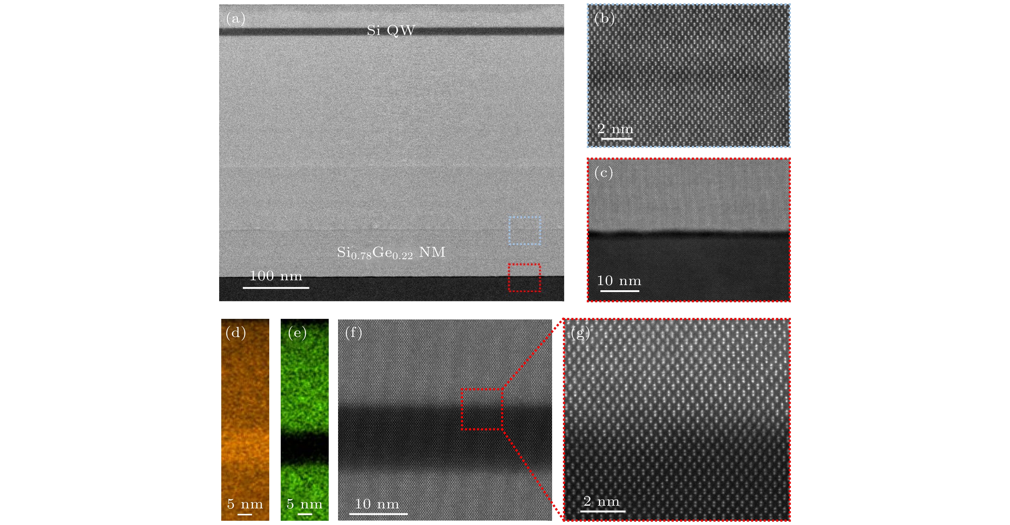
图 4 (a) Si(001)衬底上转移Si0.78Ge0.22纳米薄膜上生长Si/SiGe异质结后的截面STEM-HAADF原子图像; (b) 转移Si0.78Ge0.22纳米薄膜与外延Si0.78Ge0.22薄膜的截面STEM-HAADF原子图像; (c) Si衬底与Si0.78Ge0.22纳米薄膜界面的高倍STEM-HAADF原子图像; (d) Si量子阱附近的Si元素EDS谱; (e) Si量子阱附近的Ge元素EDS谱; (f) Si量子阱附近的高倍STEM-HAADF原子图像; (g) Si量子阱与Si0.78Ge0.22界面处的STEM-HAADF原子图像
Figure 4. (a) STEM-HAADF image after growing Si/SiGe heterostructure on transferred Si0.78Ge0.22 nanomembrane on Si (001); (b) STEM-HAADF image showing the interface between the transferred and epitaxial Si0.78Ge0.22; (c) high-magnified STEM-HAADF image showing the interface between the Si substrate and transferred Si0.78Ge0.22 nanomembrane; (d) EDS spectrum of Si element near the Si quantum well; (e) EDS spectrum of Ge element near the Si quantum well; (f) high-magnified STEM-HAADF image near the Si quantum well; (g) STEM-HAADF atomic image showing the interface between the Si quantum well and the Si0.78Ge0.22 spacer layer.
-
[1] Theis T N, Wong H S P 2017 Comput. Sci. Eng. 19 41
Google Scholar
[2] Shalf J 2020 Philos. Trans. R. Soc. Math. Phys. Eng. Sci. 378 20190061
Google Scholar
[3] Thompson S E, Parthasarathy S 2006 Mater. Today 9 20
Google Scholar
[4] Arienzo M, Iyer S S, Meyerson B S, Patton G L, Stork J M C 1991 Appl. Surf. Sci. 48 377
Google Scholar
[5] Azevedo A M D, Lopes T J, Cardoso D D, Monterio S N, Silveira P C R, Figueiredo A B H D S 2024 Obs. Econ. Latinoam. 22 e8370
Google Scholar
[6] Cressler J D 1998 IEEE Trans. Microw. Theory Tech. 46 572
Google Scholar
[7] Harame D L, Koester S J, Freeman G, Cottrel P, Rim K, Dehlinger G, Ahlgren D, Dunn J S, Greenberg D, Joseph A, Anderson F, Rieh J S, Onge S A S T, Coolbaugh D, Ramachandran V, Cressler J D, Subbanna S 2004 Appl. Surf. Sci. 224 9
Google Scholar
[8] Soref R A 1993 Proc. IEEE 81 1687
Google Scholar
[9] Wang K L, Cha D, Liu J, Chen C 2007 Proc. IEEE 95 1866
Google Scholar
[10] 张结印, 高飞, 张建军 2021 70 217802
Google Scholar
Zhang J Y, Gao F, Zhang J J 2021 Acta Phys. Sin. 70 217802
Google Scholar
[11] Tai C T, Li J Y 2024 Mater. Quantum Technol. 4 012001
Google Scholar
[12] Connors E J, Nelson J, Edge L F, Nichol J M 2022 Nat. Commun. 13 940
Google Scholar
[13] Bian H, Goh Y Y, Liu Y, Ling H, Xie L, Liu X 2021 Adv. Mater. 33 2006469
Google Scholar
[14] Fitzgerald E A, Xie Y H, Green M L, Brasen D, Kortan A R, Michel J, Mii Y J, Weir B E 1991 Appl. Phys. Lett. 59 811
Google Scholar
[15] Hartmann J M, Gallas B, Zhang J, Harris J J, Joyce B A 1999 J. Appl. Phys. 86 845
Google Scholar
[16] Rahman M M, Matada H, Tambo T, Tatsuyama C 2001 Appl. Surf. Sci. 175 6
Google Scholar
[17] Nelson S F, Ismail K, Nocera J J, Fang F F, Mendez E E, Chu J O, Meyerson B S 1992 Appl. Phys. Lett. 61 64
Google Scholar
[18] 耿鑫, 张结印, 卢文龙, 明铭, 刘方泽, 符彬啸, 褚逸昕, 颜谋回, 王保传, 张新定, 郭国平, 张建军 2024 73 117302
Google Scholar
Geng X, Zhang J Y, Lu W L, Ming M, Liu F Z, Fu B X, Chu Y X, Yan M H, Wang B C, Zhang X D, Guo G P, Zhang J J 2024 Acta Phys. Sin. 73 117302
Google Scholar
[19] Xie Y H, Fitzgerald E A, Mii Y J, Monroe D, Thiel F A, Weir B E, Feldman L C 1991 MRS Proc. 220 413
Google Scholar
[20] Ismail K 1996 J. Vac. Sci. Technol. B Microelectron. Nanometer Struct. Process. Meas. Phenom. 14 2776
Google Scholar
[21] Monroe D, Xie Y H, Fitzgerald E A, Silverman P J, Watson G P 1993 J. Vac. Sci. Technol. B Microelectron. Nanometer Struct. Process. Meas. Phenom. 11 1731
Google Scholar
[22] Paskiewicz D M, Tanto B, Savage D E, Lagally M G 2011 ACS Nano 5 5814
Google Scholar
[23] Li Y S, Sookchoo P, Cui X, Mohr R, Savage D E, Foote R H, Jacobson R, Sánchez-Pérez J R, Paskiewicz D M, Wu X, Ward D R, Coppersmith S N, Eriksson M A, Lagally M G 2015 ACS Nano 9 4891
Google Scholar
[24] Schäffler F 1997 Semicond. Sci. Technol. 12 1515
Google Scholar
[25] Schmidt O G, Eberl K 2001 Nature 410 168
Google Scholar
[26] Wolf I D 1996 Semicond. Sci. Technol. 11 139
Google Scholar
[27] Pezzoli F, Bonera E, Grilli E, Guzzi M, Sanguinetti S, Chrastina D, Isella G, Von Känel H, Wintersberger E, Stangl J, Bauer G 2008 J. Appl. Phys. 103 093521
Google Scholar
[28] Nakashima S, Mitani T, Ninomiya M, Matsumoto K 2006 J. Appl. Phys. 99 053512
Google Scholar
[29] Wong L H, Wong C C, Liu J P, Sohn D K, Chan L, Hsia L C, Zang H, Ni Z H, Shen Z X 2005 Jpn. J. Appl. Phys. 44 7922
Google Scholar
[30] Loup V, Gabette L, Roure M C, Kachtouli R, Jourdan M, Besson P, Petitdidier S 2013 ECS Trans. 58 47
Google Scholar
[31] Shikida M, Sato K, Tokoro K, Uchikawa D 2000 Sens. Actuators Phys. 80 179
Google Scholar


 DownLoad:


Catalog
Metrics
- Abstract views: 533
- PDF Downloads: 19
- Cited By: 0
