


-
Photodetector occupies an important position in the sensor family, but most of the photoelectric conversion materials of photodetectors are inorganic semiconductors, such as GaAs, GaN, Ge and Si, these inorganic semiconductors are usually prepared by complicated methods and high cost, and furthermore, they have poor mechanical flexibility. Organic-inorganic hybrid perovskite materials serving as visible-light sensitizers have the advantages of balanced electron and hole mobilities, adjustable bandgaps, high absorption coefficients, low temperature solution preparation, which make the materials a suitable candidate for inorganic semiconductors. For planar photodetectors, carriers have greater probabilities to be trapped by the defects in the perovskite films, therefore it is important to fabricate a high-quality perovskite film. However, owing to the low formation energy of perovskite crystals, defects prove to occur on the film surface and grain boundaries, which aggravate the performance of perovskite optoelectronic devices. In this work, we introduce a small quantity of graphene oxide nanosheets (GOSs) on bare glass substrate as effective nucleation sites of perovskite crystals. Owing to the extremely low density of GOSs and large exposed glass basement, the GOSs cannot be regarded as an interface layer. The existence of GOSs on smooth substance reduces the perovskite nucleation barrier, leading to a more preferential crystal growth in these locations, and binds tightly with glass substrate, which passivates the defects efficiently. Meanwhile, the element of O in the GOSs can create Pb–O bond with Pb in the CH3NH3PbI3, further improving the crystal of perovskite. On this basis, planner perovskite photodetector with a structure of glass/GOSs/CH3NH3PbI3/MoO3/Au is fabricated. By adjusting the concentration of GOSs deionized water dispersion under the same spin-coating condition, the photoelectric conversion performance of perovskite photodetector is enhanced. Under the influence of the optimal concentration of GOSs, photocurrent of the champion photodetector (1.15 × 10⁻⁶ A) is an order of magnitude higher than that of reference device without GOSs modified (3.58 × 10⁻⁷ A) at 3 V bias, leading to a high ON/OFF current ratio of 5.22 × 10³. Besides, improved photoresponse speed is also found in the champion device, with a rise time of 9.6 ms and a decay time of 6.6 ms, respectively. The enhanced performance of GOSs modified perovskite photodetector can be attributed to the significantly reduced defects bringing about an enhanced charge separation and collection performance in the CH3NH3PbI3 films. By introducing extremely low quantity GOSs as the effective perovskite crystal nucleation sites, the perovskite crystallization and thin film can be effectively improved, leading to a positive effect on the performance of perovskite photodetector. This method has a certain universality, and therefore it has a reference value for other structures of perovskite photoelectric devices. [1] Šagátová A, Zaťko B, Nečas V, Dubecký F, Anh T L, Sedlačková K, Boháček P, Zápražný Z 2018 Appl. Surf. Sci. 461 3
 Google Scholar
[2] Tian H J, Hu A Q, Liu Q L, He X Y, Guo X 2020 Adv. Opt. Mater. 8 1901741
Google Scholar
[3] Wu J H, Yang Z W, Qiu C Y, Zhang Y J, Wu Z Q, Yang J L, Lu Y H, Li J F, Yang D X, Hao R, Li E P, Yu G L, Lin S S 2018 Nanoscale 10 8023
Google Scholar
[4] Gundimeda A, Krishna S, Aggarwal N, Sharma A, Sharma N D, Maurya K K, Husale S, Gupta G 2017 Appl. Phys. Lett. 110 103507
Google Scholar
[5] Liu L, Yang C, Patanè A, Yu Z, Yan F G, Wang K Y, Lu H X, Li J M, Zhao L X 2017 Nanoscale 9 8142
Google Scholar
[6] Takenaka M, Morii K, Sugiyama M, Nakano Y, Takagi S 2012 Opt. Express 20 8718
Google Scholar
[7] Hössbacher C, Salamin Y, Fedoryshyn Y, et al. 2017 IEEE Photonics Technol. Lett. 29 1760
Google Scholar
[8] Berencén Y, Prucnal S, Liu F, Skorupa I, Hübner R, Rebohle L, Zhou S Q, Schneider H, Helm M, Skorupa W 2017 Sci. Rep. 7 1
Google Scholar
[9] Vivien L, Polzer A, Marris-Morini D, Osmond J, Hartmann J M, Crozat P, Cassan E, Kopp C, Zimmermann H, Fédéli J M 2012 Opt. Express 20 1096
Google Scholar
[10] Yang J, Pi M Y, Zhang D K, Tang X S, Du J 2021 Chin. J. Lumin. 42 755
Google Scholar
[11] Gayen R N, Paul R, Biswas S 2020 Appl. Surf. Sci. 533 147149
Google Scholar
[12] Ozel K, Yildiz A 2021 Phys. Status. Solidi RRL 15 2100085
Google Scholar
[13] Chen W, Tang H, Chen Y, Heger J E, Li N, Kreuzer L P, Xie Y, Li D P, Anthony C, Pikramenou Z, Ng W K, Sun X W, Wang K, Müller-Buschbaum, P 2020 Nano Energy 78 105254
Google Scholar
[14] Wang Y D, Liu Y L, Cao S K, Wang J Z 2021 J. Mater. Chem. C 9 5302
Google Scholar
[15] 柴磊, 钟敏 2016 65 237902
Google Scholar
Chai L, Zhong M 2016 Acta Phys. Sin. 65 237902
Google Scholar
[16] Qu Z H, Ma F, Zhao Y, Chu X B, Yu S Q, You J B 2021 Chin. Phys. Lett. 38 107801
Google Scholar
[17] Wang H, Kim D H 2017 Chem. Soc. Rev. 46 5204
Google Scholar
[18] 张钰, 周欢萍 2019 68 158804
Google Scholar
Zhang Y, Zhou H P 2019 Acta Phys. Sin. 68 158804
Google Scholar
[19] Zhu H L, Liang Z, Huo Z, Ng W K, Mao J, Wong K S, Yin W J, Choy W C H 2018 Adv. Funct. Mater. 28 1706068
Google Scholar
[20] Li Y, Li Y, Shi J, Zhang H Y, Wu J H, Li D M, Luo Y H, Wu H J, Meng Q B 2018 Adv. Funct. Mater. 28 1705220
Google Scholar
[21] Wang T, Lian G, Huang L P, Zhu F, Cui D L, Wang Q L, Meng Q B, Jiang H H, Zhou G J, Wong C P 2019 Nano Energy 64 103914
Google Scholar
[22] Li D, Müller M B, Gilje S, Kaner R B, Wallace G G 2008 Nat. Nanotechnol. 3 101
Google Scholar
[23] Yang X, Qiu L, Cheng C, Wu Y Z, Ma Z F, Li D 2011 Angew. Chem. Int. Ed. 50 7325
Google Scholar
[24] Georgakilas V, Tiwari J N, Kemp K C, Perman J A, Bourlinos A B, Kim K S, Zboril R 2016 Chem. Rev. 116 5464
Google Scholar
[25] Ye S Y, Rao H X, Yan W B, Li Y H, Sun W H, Peng H T, Liu Z W, Bian Z Q, Li Y F, Huang C H 2016 Adv. Mater. 28 9648
Google Scholar
[26] Jeon N J, Noh J H, Kim Y C, Yang W S, Ryu S, Seol S I 2014 Nat. Mater. 13 897
Google Scholar
[27] Wang Z K, Li M, Yuan D X, Shi X B, Ma H, Liao L S 2015 ACS Appl. Mater. Interfaces 7 9645
Google Scholar
[28] Liu L, Xi Q Y, Gao G, Yang W, Zhou H, Zhao Y X, Wu C Q, Wang L D, Xu J W 2016 Sol. Energy Mater. Sol. Cells 157 937
Google Scholar
[29] Li W Z, Dong H P, Guo X D, Li N, Li J W, Niu G D, Wang L D 2014 J. Mater. Chem. A 2 20105
Google Scholar
[30] Kröger M, Hamwi S, Meyer J, Riedl T, Kowalsky W, Kahn A 2009 Appl. Phys. Lett. 95 251
[31] Greiner M T, Helander M G, Tang W M, Wang Z B, Qiu J, Lu Z H 2012 Nat. Mater. 11 76
Google Scholar
[32] Wang Y, Song Q G, Lin T, Fu Y, Sun X, Chu B, Jin F M, Zhao H F, Li W L, Su Z S, Li Y T 2017 Org. Electron. 49 355
Google Scholar
[33] Afzal A M, Bae I G, Aggarwal Y, Park J, Jeong H R, Choi E H, Park B 2021 Sci. Rep. 11 1
Google Scholar
[34] Hamilton M C, Martin S, Kanicki J 2004 IEEE Trans. Electron. Devices 51 887
[35] Khan A A, Azam M, Eric D, Liang G X, Yu Z N 2020 J. Mater. Chem. C 8 2880
Google Scholar
[36] Wei Y Z, Feng G T, Mao P, Luan Y G, Zhuang J, Chen N L, Yang H X, Li W W, Yang S Y, Wang J Z 2020 ACS Appl. Mater. Interfaces 12 8826
Google Scholar
[37] Shan C W, Meng F, Yu J H, Wang Z X, Li W H, Fan D Y, Chen R, Ma H B, Li G Q, Kyaw A K K 2021 J. Mater. Chem. C 9 7632
Google Scholar
[38] Srivastava A, Jit S, Tripathi S 2021 IEEE Trans. Electron. Devices 68 IEEE Trans. Electron. Devices
[39] Reddy K C S, Selamneni V, Rao M G S, Meza-Arroyo J, Sahatiya P, Ramirez-Bon R 2021 Appl. Surf. Sci. 568 150944
Google Scholar
[40] Dutta A, Medda A, Bera R, Sarkar K, Sain S, Kumar P, Patra A 2020 ACS Appl. Nano Mater. 3 4717
[41] Bristow H, Jacoutot P, Scaccabarozzi A D, et al. 2020 ACS Appl. Mater. Interfaces 12 48836
Google Scholar
-
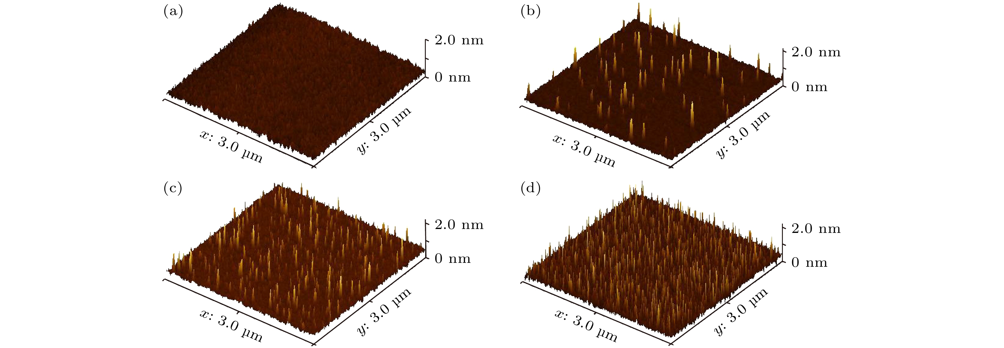
图 1 (a) 空白硅片以及 (b) 0.025, (c) 0.050, (d) 0.100 mg/mL GOSs分散液沉积在硅片表面的形貌
Figure 1. The morphology of (a) bare silicon wafer and (b) 0.025, (c) 0.050, (d) 0.100 mg/ mL GOSs dispersion deposited on the surface of silicon wafer.
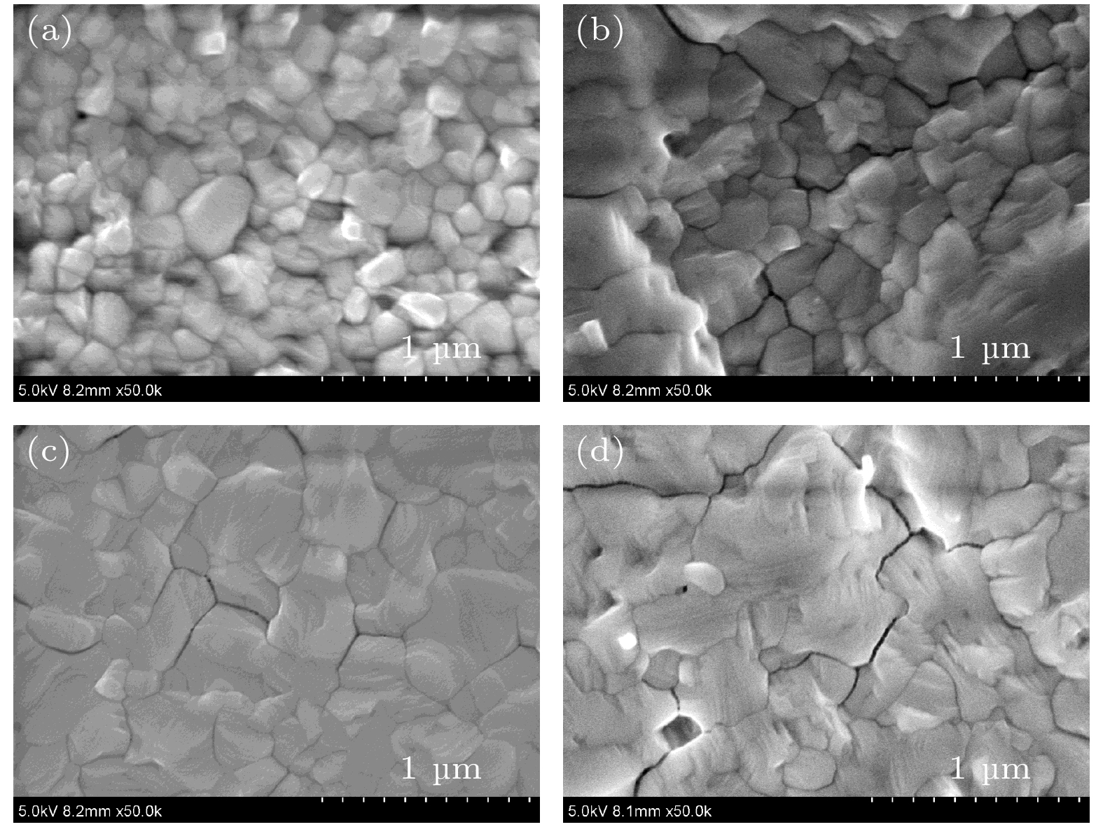
图 2 (a) G0, (b) G0.025, (c) G0.05和(d) G0.1上生长的钙钛矿薄膜的平面扫描SEM照片
Figure 2. Top-view SEM images of the CH3NH3PbI3 films on (a) G0, (b) G0.025, (c) G0.05 and (d) G0.1
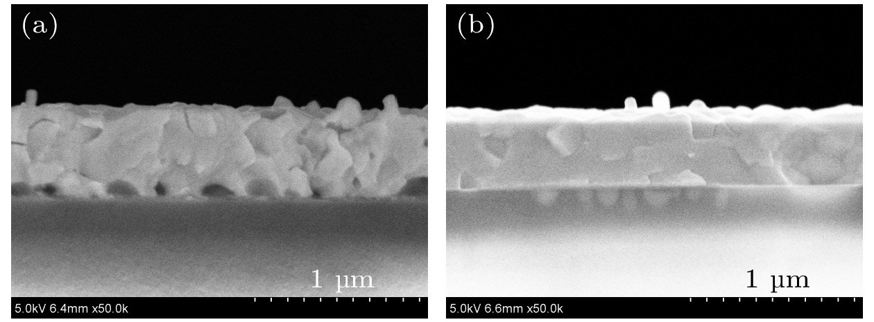
图 3 (a) G0和(b) G0.05上生长的钙钛矿薄膜的断面扫描SEM照片
Figure 3. Cross-sectional SEM images of the CH3NH3PbI3 films on (a) G0 and (b) G0.05
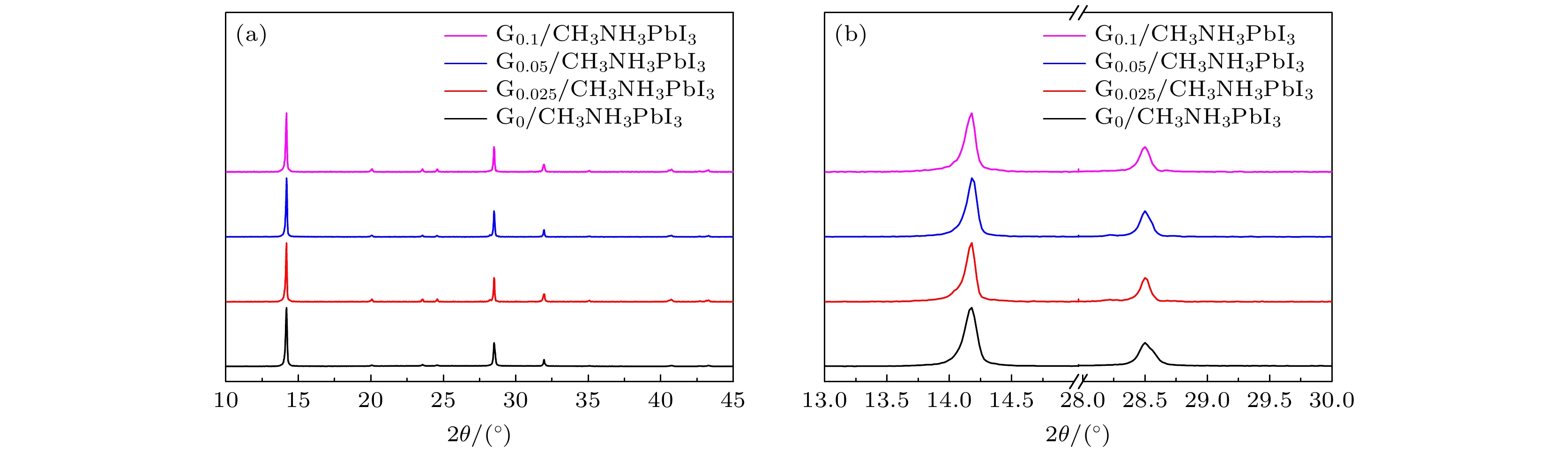
图 4 (a) 钙钛矿薄膜在G0, G0.025, G0.05以及G0.1上的XRD图谱; (b) 相应样品在14.2°和28.5°位置衍射峰放大图
Figure 4. (a) XRD patterns of the CH3NH3PbI3 films on G0, G0.025, G0.05 and G0.1; (b) enlarged diffraction peaks at 14.2° and 28.5° of the corresponding samples.
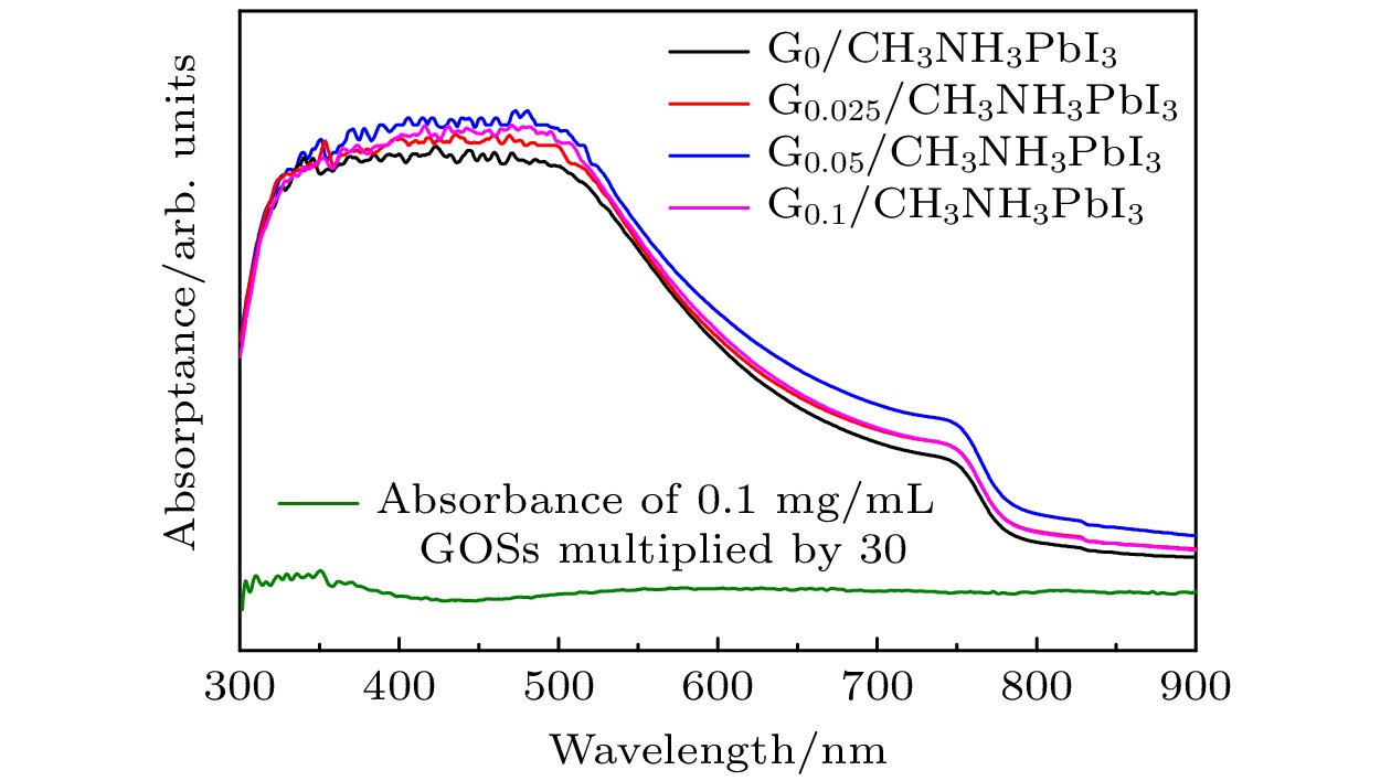
图 5 沉积在G0, G0.025, G0.05以及G0.1上的CH3NH3PbI3光吸收谱. 图中同时给出G0.1放大30倍的吸收光谱
Figure 5. Absorbance spectra of the CH3NH3PbI3 films deposited on G0, G0.025, G0.05 and G0.1. The absorption spectrum of G0.1 amplified by 30 is also shown in the figure.
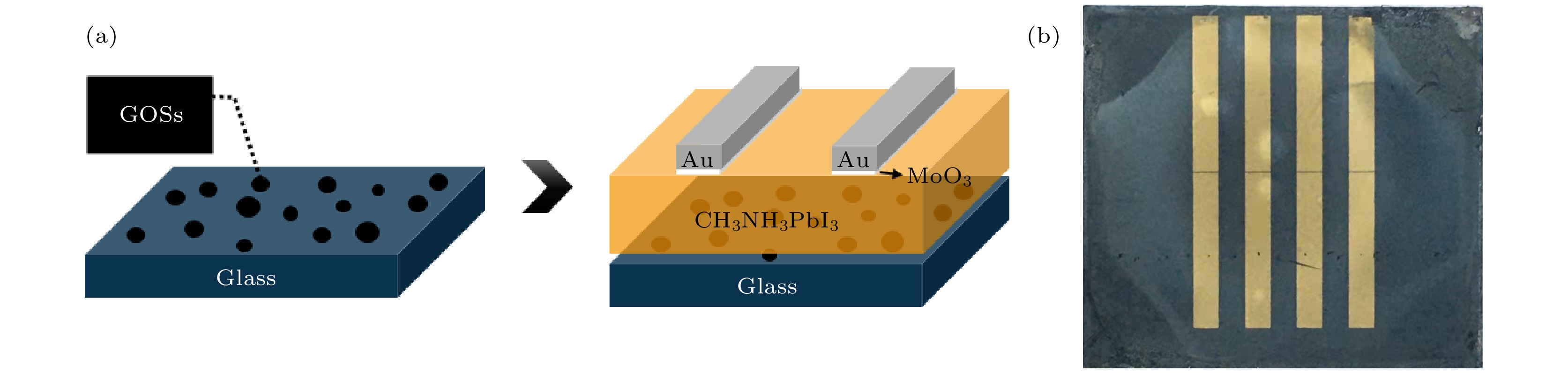
图 6 钙钛矿光电探测器的(a)结构示意图和(b)器件实物照片
Figure 6. (a) Schematic structure and (b) picture of the perovskite photodetector.
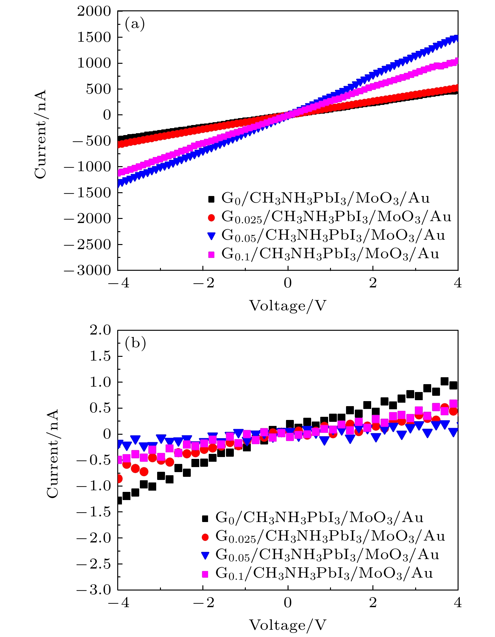
图 7 (a)光照及(b)黑暗条件下G0, G0.025, G0.05和G0.1上制备的钙钛矿探测器的I-V曲线
Figure 7. I-V curves of the photodetectors fabricated on G0, G0.025, G0.05 and G0.1 under (a) solar simulator irradiation and (b) dark, respectively.
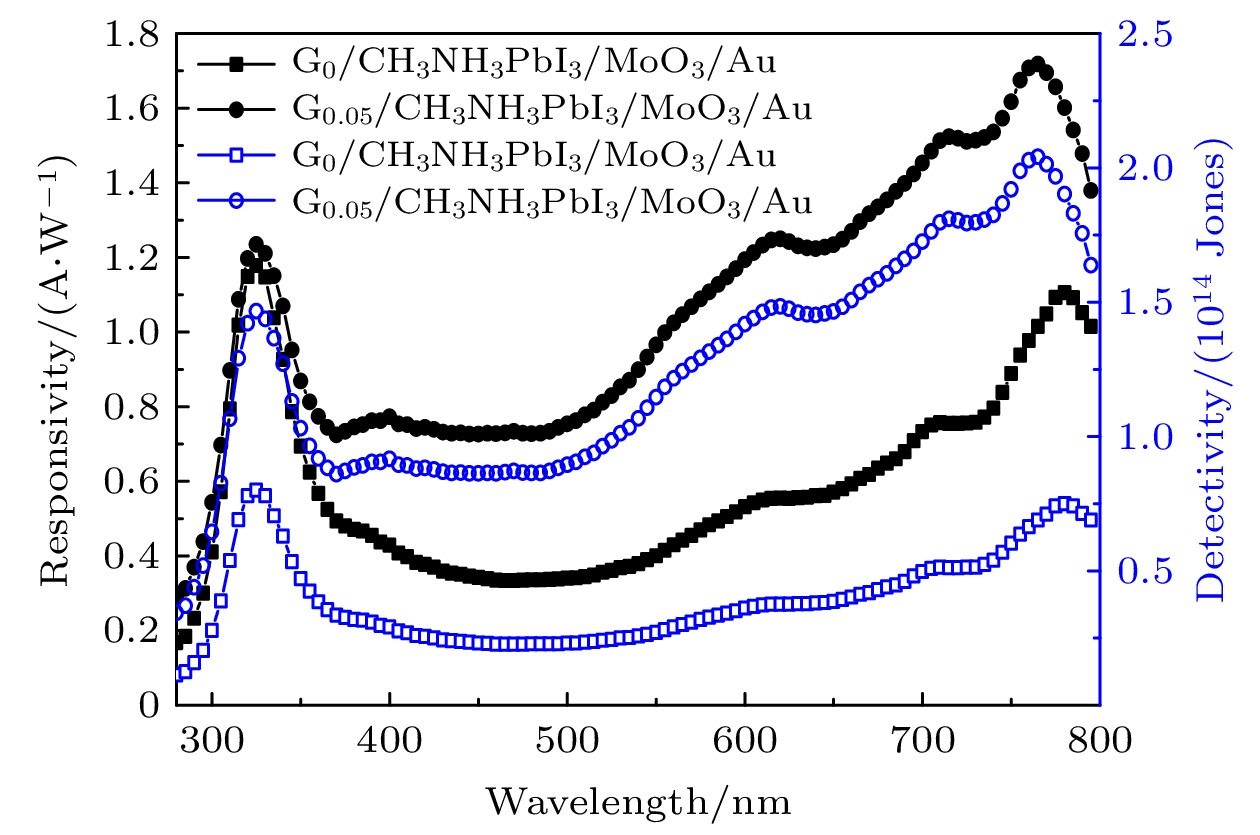
图 8 分别沉积在G0和G0.05上的钙钛矿光电探测器的R和D*
Figure 8. The R and D* of perovskite photodetectors fabricated on G0 and G0.05, respectively.
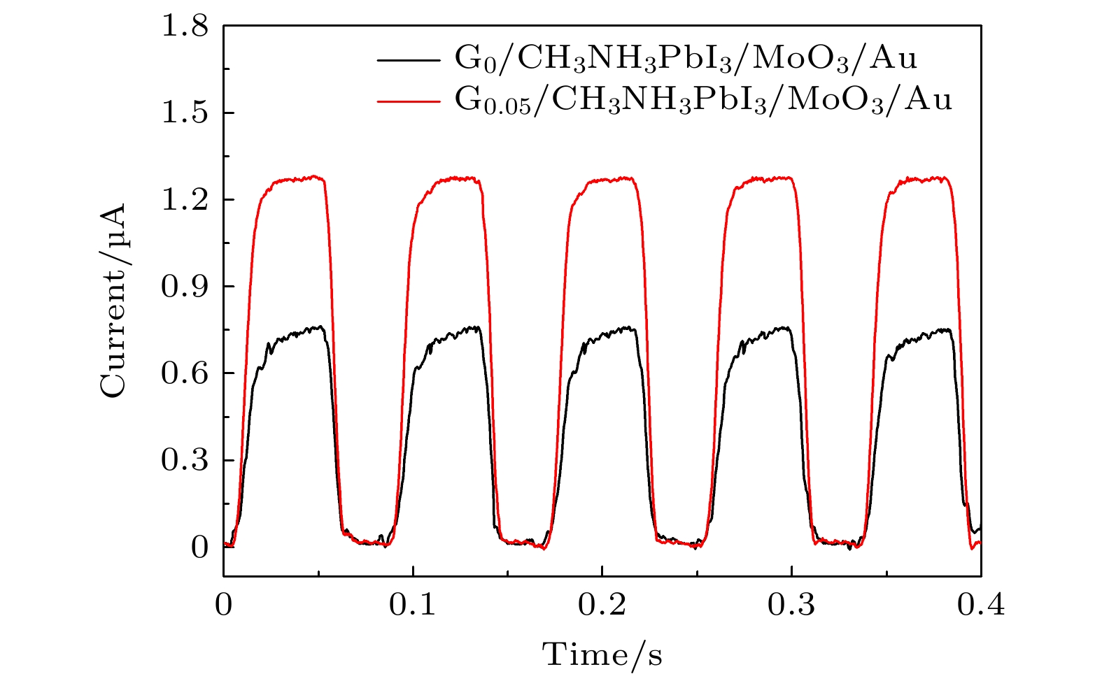
图 9 G0和G0.05上制备的钙钛矿光电探测器的5个周期光响应行为
Figure 9. Five cycles photoresponse behavious of the perovskite photodetectors fabricated on G0 and G0.05.
表 1 不同基底上生长的钙钛矿薄膜XRD衍射峰半峰宽
Table 1. FWHM of the CH3NH3PbI3 XRD diffraction peaks deposited on different substrates.
FWHM/(°) 14.2 28.5 G0/CH3NH3PbI3 0.133 0.146 G0.025/CH3NH3PbI3 0.113 0.104 G0.05/CH3NH3PbI3 0.112 0.099 G0.1/CH3NH3PbI3 0.121 0.115  DownLoad: CSV
表 2 溶液法制备的可见光探测器性能
Table 2. Performance of visible light detector prepared by solution method.
材料 制备方法 开关比/103 响应度/(A·W–1) 探测率/Jones 响应时间 Ref. Cs0.1FA0.2MA0.7Pb(I0.9Cl0.1)3-F4TCNQ 旋涂 6.94 5.4 — 530 ms/600 ms [35] (BA)2(MA)n1PbnI3n+1 旋涂 1.38 27.06 — 3.53 ms/3.78 ms [36] CH3NH3PbI3 旋涂 — 0.47 8.2 × 10¹² 18 ns [37] CH3NH3PbI3 旋涂 5.22 1.71 2.04 × 10¹⁴ 9.6 ms/6.6 ms This work ZnO/pentacene 旋涂 — 0.36 2.17 × 10¹⁴ — [38] p-NiO/n-CdS 水热法/旋涂 ~0.005 2.60 × 10⁻² 9.21 × 10⁹ 3.5 s [39] CdSe 旋涂 4.7 0.16 4 × 10¹¹ 107 ms/110 ms [40] PTQ10∶O-IDTBR 刮刀涂布 — 0.03 3.3 × 10¹¹ 20 μs/25 μs [41] PTQ10∶O-FBR 0.34 9.6 × 10¹² 12 μs/15 μs
DownLoad: CSV
-
[1] Šagátová A, Zaťko B, Nečas V, Dubecký F, Anh T L, Sedlačková K, Boháček P, Zápražný Z 2018 Appl. Surf. Sci. 461 3
Google Scholar
[2] Tian H J, Hu A Q, Liu Q L, He X Y, Guo X 2020 Adv. Opt. Mater. 8 1901741
Google Scholar
[3] Wu J H, Yang Z W, Qiu C Y, Zhang Y J, Wu Z Q, Yang J L, Lu Y H, Li J F, Yang D X, Hao R, Li E P, Yu G L, Lin S S 2018 Nanoscale 10 8023
Google Scholar
[4] Gundimeda A, Krishna S, Aggarwal N, Sharma A, Sharma N D, Maurya K K, Husale S, Gupta G 2017 Appl. Phys. Lett. 110 103507
Google Scholar
[5] Liu L, Yang C, Patanè A, Yu Z, Yan F G, Wang K Y, Lu H X, Li J M, Zhao L X 2017 Nanoscale 9 8142
Google Scholar
[6] Takenaka M, Morii K, Sugiyama M, Nakano Y, Takagi S 2012 Opt. Express 20 8718
Google Scholar
[7] Hössbacher C, Salamin Y, Fedoryshyn Y, et al. 2017 IEEE Photonics Technol. Lett. 29 1760
Google Scholar
[8] Berencén Y, Prucnal S, Liu F, Skorupa I, Hübner R, Rebohle L, Zhou S Q, Schneider H, Helm M, Skorupa W 2017 Sci. Rep. 7 1
Google Scholar
[9] Vivien L, Polzer A, Marris-Morini D, Osmond J, Hartmann J M, Crozat P, Cassan E, Kopp C, Zimmermann H, Fédéli J M 2012 Opt. Express 20 1096
Google Scholar
[10] Yang J, Pi M Y, Zhang D K, Tang X S, Du J 2021 Chin. J. Lumin. 42 755
Google Scholar
[11] Gayen R N, Paul R, Biswas S 2020 Appl. Surf. Sci. 533 147149
Google Scholar
[12] Ozel K, Yildiz A 2021 Phys. Status. Solidi RRL 15 2100085
Google Scholar
[13] Chen W, Tang H, Chen Y, Heger J E, Li N, Kreuzer L P, Xie Y, Li D P, Anthony C, Pikramenou Z, Ng W K, Sun X W, Wang K, Müller-Buschbaum, P 2020 Nano Energy 78 105254
Google Scholar
[14] Wang Y D, Liu Y L, Cao S K, Wang J Z 2021 J. Mater. Chem. C 9 5302
Google Scholar
[15] 柴磊, 钟敏 2016 65 237902
Google Scholar
Chai L, Zhong M 2016 Acta Phys. Sin. 65 237902
Google Scholar
[16] Qu Z H, Ma F, Zhao Y, Chu X B, Yu S Q, You J B 2021 Chin. Phys. Lett. 38 107801
Google Scholar
[17] Wang H, Kim D H 2017 Chem. Soc. Rev. 46 5204
Google Scholar
[18] 张钰, 周欢萍 2019 68 158804
Google Scholar
Zhang Y, Zhou H P 2019 Acta Phys. Sin. 68 158804
Google Scholar
[19] Zhu H L, Liang Z, Huo Z, Ng W K, Mao J, Wong K S, Yin W J, Choy W C H 2018 Adv. Funct. Mater. 28 1706068
Google Scholar
[20] Li Y, Li Y, Shi J, Zhang H Y, Wu J H, Li D M, Luo Y H, Wu H J, Meng Q B 2018 Adv. Funct. Mater. 28 1705220
Google Scholar
[21] Wang T, Lian G, Huang L P, Zhu F, Cui D L, Wang Q L, Meng Q B, Jiang H H, Zhou G J, Wong C P 2019 Nano Energy 64 103914
Google Scholar
[22] Li D, Müller M B, Gilje S, Kaner R B, Wallace G G 2008 Nat. Nanotechnol. 3 101
Google Scholar
[23] Yang X, Qiu L, Cheng C, Wu Y Z, Ma Z F, Li D 2011 Angew. Chem. Int. Ed. 50 7325
Google Scholar
[24] Georgakilas V, Tiwari J N, Kemp K C, Perman J A, Bourlinos A B, Kim K S, Zboril R 2016 Chem. Rev. 116 5464
Google Scholar
[25] Ye S Y, Rao H X, Yan W B, Li Y H, Sun W H, Peng H T, Liu Z W, Bian Z Q, Li Y F, Huang C H 2016 Adv. Mater. 28 9648
Google Scholar
[26] Jeon N J, Noh J H, Kim Y C, Yang W S, Ryu S, Seol S I 2014 Nat. Mater. 13 897
Google Scholar
[27] Wang Z K, Li M, Yuan D X, Shi X B, Ma H, Liao L S 2015 ACS Appl. Mater. Interfaces 7 9645
Google Scholar
[28] Liu L, Xi Q Y, Gao G, Yang W, Zhou H, Zhao Y X, Wu C Q, Wang L D, Xu J W 2016 Sol. Energy Mater. Sol. Cells 157 937
Google Scholar
[29] Li W Z, Dong H P, Guo X D, Li N, Li J W, Niu G D, Wang L D 2014 J. Mater. Chem. A 2 20105
Google Scholar
[30] Kröger M, Hamwi S, Meyer J, Riedl T, Kowalsky W, Kahn A 2009 Appl. Phys. Lett. 95 251
[31] Greiner M T, Helander M G, Tang W M, Wang Z B, Qiu J, Lu Z H 2012 Nat. Mater. 11 76
Google Scholar
[32] Wang Y, Song Q G, Lin T, Fu Y, Sun X, Chu B, Jin F M, Zhao H F, Li W L, Su Z S, Li Y T 2017 Org. Electron. 49 355
Google Scholar
[33] Afzal A M, Bae I G, Aggarwal Y, Park J, Jeong H R, Choi E H, Park B 2021 Sci. Rep. 11 1
Google Scholar
[34] Hamilton M C, Martin S, Kanicki J 2004 IEEE Trans. Electron. Devices 51 887
[35] Khan A A, Azam M, Eric D, Liang G X, Yu Z N 2020 J. Mater. Chem. C 8 2880
Google Scholar
[36] Wei Y Z, Feng G T, Mao P, Luan Y G, Zhuang J, Chen N L, Yang H X, Li W W, Yang S Y, Wang J Z 2020 ACS Appl. Mater. Interfaces 12 8826
Google Scholar
[37] Shan C W, Meng F, Yu J H, Wang Z X, Li W H, Fan D Y, Chen R, Ma H B, Li G Q, Kyaw A K K 2021 J. Mater. Chem. C 9 7632
Google Scholar
[38] Srivastava A, Jit S, Tripathi S 2021 IEEE Trans. Electron. Devices 68 IEEE Trans. Electron. Devices
[39] Reddy K C S, Selamneni V, Rao M G S, Meza-Arroyo J, Sahatiya P, Ramirez-Bon R 2021 Appl. Surf. Sci. 568 150944
Google Scholar
[40] Dutta A, Medda A, Bera R, Sarkar K, Sain S, Kumar P, Patra A 2020 ACS Appl. Nano Mater. 3 4717
[41] Bristow H, Jacoutot P, Scaccabarozzi A D, et al. 2020 ACS Appl. Mater. Interfaces 12 48836
Google Scholar
-
 17-20220189补充材料.pdf


 DownLoad:


Catalog
Metrics
- Abstract views: 6304
- PDF Downloads: 98
- Cited By: 0
