-
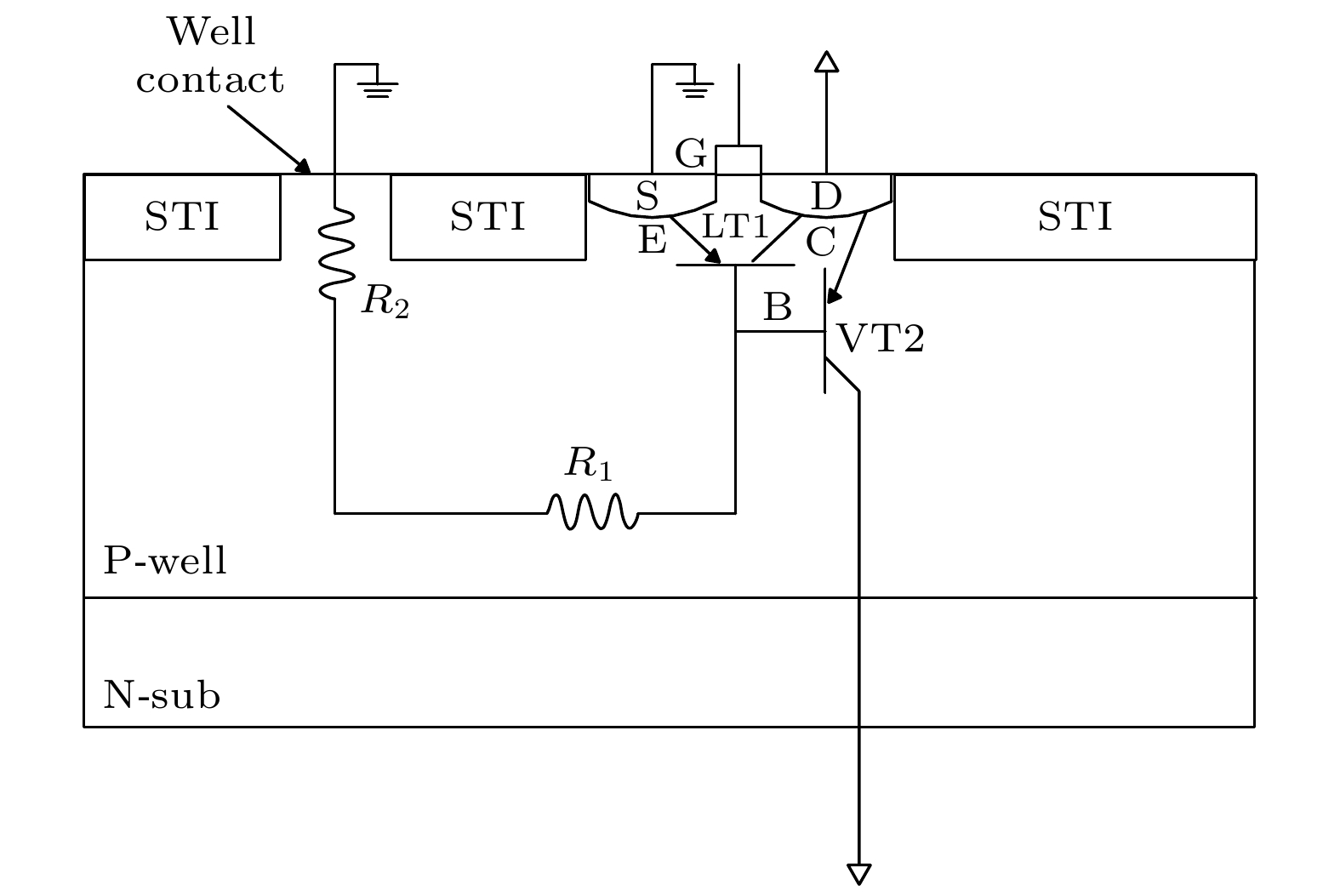
The parasitic effect inside metal oxide field effect transistor regarded as the basic structure of large scale digital circuits, has long been considered as an important factor affecting the disturbance, upset and latchup of integrated circuits in pulsed γ-ray radiation environment. To investigate the turn-on mechanism of vertical parasitic effect in NMOSFET induced by pulsed γ-ray radiation, the 40 nm, 90 nm and 180 nm NMOSFET device models are constructed by TCAD and the normal electrical characteristics are calibrated. The trend of vertical parasitic triode current gain, the turn-on conditions of vertical parasitic triode and their influence on working state of NMOSFET are obtained. The simulation results are shown below. 1) The disturbance of well potential inside NMOSFET induced by pulsed γ-ray radiation is the main reason for the turn-on of vertical parasitic triode. 2) When vertical parasitic triode is turn-on, the large secondary photocurrent will be generated inside NMOSFET which will affect the working state of the transistor. 3) The current gain of vertical parasitic triode in NMOSFET decreases with the technology node decreasing. The results provide a theoretical basis for studying the transient ionizing radiation effects of electronic devices.
-
Keywords:
- transient ionizing radiation effect /
- parasitic effect /
- rise of well potential /
- secondary photocurrent
[1] Wirth J L, Rogers S C 1964 IEEE Trans. Nucl. Sci. 11 24
 Google Scholar
[2] Enlow E W, Alexander D R 1988 IEEE Trans. Nucl. Sci. 35 1467
 Google Scholar
[3] Fjeldly T A, Deng Y Q, Shur M S, Hjalmarson H P, Muyshondt A, Ytterdal T 2001 IEEE Trans. Nucl. Sci. 48 1721
 Google Scholar
[4] Alexander D R 2003 IEEE Trans. Nucl. Sci. 50 565
 Google Scholar
[5] 赖祖武 1998 抗辐射电子学(北京: 国防工业出版社) 第288—300页
Lai Z W 1998 Radiation Electronics (Beijing: Defense Industry Press) pp288–300 (in Chinese)
[6] Lewis C 1995 Transient Radiation Effects on Electronics (Alexandria: Defense Nuclear Agency) pp200–245
[7] 马强, 林东生, 范如玉, 陈伟, 杨善潮, 龚建成, 王桂珍, 齐超 2010 原子能科学技术 44 545
 Google Scholar
Ma Q, Lin D S, Fan R Y, Chen W, Yang S C, Gong J C, Wang G Z, Qi C 2010 Atomic Energy Science and Technology 44 545
 Google Scholar
[8] Oh S C, Lee N H, Lee H H 2012 12th International Conference on Control, Automation and Systems Jeju Island, Korea, October 17–21, 2012 p1233
[9] 王桂珍, 林东生, 齐超, 白小燕, 杨善潮, 李瑞宾, 马强, 金晓明, 刘岩 2014 原子能科学技术 48 2165
 Google Scholar
Wang G Z, Lin D S, Qi C, Bai X Y, Yang S C, Li R B, Ma Q, Jin X M, Liu Y 2014 Atomic Energy Science and Technology 48 2165
 Google Scholar
[10] Massengill L W, Diehl-Nagle S E 1985 IEEE Trans. Nucl. Sci. 32 4026
 Google Scholar
[11] Massengill L W, Diehl-Nagle S E 1986 IEEE Trans. Nucl. Sci. 33 1541
 Google Scholar
[12] Li J L, Chen W, Li R B, Wang G Z, Yang S C 2019 3rd Internaltional Conference on Radiation Effects of Electronic Devices Chongqing, China, May 29–31, 2019 pp1–4
[13] Boselli G, Reddy V, Duvvury C 2005 43rd Annual International Reliability Physics Symposium San Jose, USA, April 17–21, 2005 p137
[14] Li R B, Chen W, Lin D S, Yang S C, Bai X Y, Wang G Z, Liu Y, Qi C, Ma Q 2012 Sci. Chin. Tech. Sci. 55 3242
 Google Scholar
[15] Keshavarz A A, Fischer T A, Dawes W R, Hawkins C F 1988 IEEE Trans. Nucl. Sci. 35 1422
 Google Scholar
[16] Olson B D, Amusan O A, Dasgupta S, Massengill L W, Witulski A F, Bhuva B L, Alles M L, Warrenm K M, Ball D R 2007 IEEE Trans. Nucl. Sci. 54 894
 Google Scholar
[17] Ahlbin J R, Atkinson N M, Gadlage M J, Gaspard N J, Bhuva B L, Loveless T D, Zhang E X, Chen L, Massengill L W 2011 IEEE Trans. Nucl. Sci. 58 2585
 Google Scholar
[18] 金晓明, 范如玉, 陈伟, 王桂珍, 林东生, 杨善潮, 白小燕 2010 原子能科学技术 44 1487
 Google Scholar
Jin X M, Fan R Y, Chen W, Wang G Z, Lin D S, Yang S C, Bai X Y 2010 Atomic Energy Science and Technology 44 1487
 Google Scholar
[19] Calienes W, Reis R, Anghel C, Vladimirescu A 2014 IEEE 57th International Midwest Symposium on Circuits and Systems Texas, USA, August 3–6, 2014 p655
[20] Wunsch T F, Hash G L, Hewlett F W, Treece R K 1991 IEEE Trans. Nucl. Sci. 38 1392
 Google Scholar
[21] Dasgupta S 2007 M. S. Thesis (Nashville: Vanderbilt University)
[22] Atkinson N M 2010 M. S. Thesis (Nashville: Vanderbilt University)
[23] Li R B, Wang C H, He C H, Chen W, Li J L, Qi C, Liu Y 2020 Nucl. Instrum. Meth. B 470 32
 Google Scholar
[24] Neamen D A 2007 Semiconductor Physics and Devices Basic Principles (Beijing: Publishing House of Electronics Industry) pp284–285
-
表 1 不同尺寸NMOS管结构参数与工艺参数
Table 1. Structure and process parameters of NMOS with different feature size.
工艺节点
λ/nm沟道长度
L/nm沟道宽度
W/nm源漏掺杂
/cm3晕掺杂
/cm3多晶硅掺杂
/cm3阈值掺杂
/cm3漏电掺杂
/cm340 40 120 2 × 10²⁰ 1.5 × 10¹⁹ 2 × 10²⁰ 7.5 × 10¹⁸ 7.5 × 10¹⁸ 90 80 200 2 × 10²⁰ 1 × 10¹⁸ 2 × 10²⁰ 8.2 × 10¹⁸ 8 × 10¹⁸ 180 180 540 1 × 10²⁰ 8 × 10¹⁷ 1 × 10²⁰ 8 × 10¹⁸ 7 × 10¹⁸ -
[1] Wirth J L, Rogers S C 1964 IEEE Trans. Nucl. Sci. 11 24
 Google Scholar
[2] Enlow E W, Alexander D R 1988 IEEE Trans. Nucl. Sci. 35 1467
 Google Scholar
[3] Fjeldly T A, Deng Y Q, Shur M S, Hjalmarson H P, Muyshondt A, Ytterdal T 2001 IEEE Trans. Nucl. Sci. 48 1721
 Google Scholar
[4] Alexander D R 2003 IEEE Trans. Nucl. Sci. 50 565
 Google Scholar
[5] 赖祖武 1998 抗辐射电子学(北京: 国防工业出版社) 第288—300页
Lai Z W 1998 Radiation Electronics (Beijing: Defense Industry Press) pp288–300 (in Chinese)
[6] Lewis C 1995 Transient Radiation Effects on Electronics (Alexandria: Defense Nuclear Agency) pp200–245
[7] 马强, 林东生, 范如玉, 陈伟, 杨善潮, 龚建成, 王桂珍, 齐超 2010 原子能科学技术 44 545
 Google Scholar
Ma Q, Lin D S, Fan R Y, Chen W, Yang S C, Gong J C, Wang G Z, Qi C 2010 Atomic Energy Science and Technology 44 545
 Google Scholar
[8] Oh S C, Lee N H, Lee H H 2012 12th International Conference on Control, Automation and Systems Jeju Island, Korea, October 17–21, 2012 p1233
[9] 王桂珍, 林东生, 齐超, 白小燕, 杨善潮, 李瑞宾, 马强, 金晓明, 刘岩 2014 原子能科学技术 48 2165
 Google Scholar
Wang G Z, Lin D S, Qi C, Bai X Y, Yang S C, Li R B, Ma Q, Jin X M, Liu Y 2014 Atomic Energy Science and Technology 48 2165
 Google Scholar
[10] Massengill L W, Diehl-Nagle S E 1985 IEEE Trans. Nucl. Sci. 32 4026
 Google Scholar
[11] Massengill L W, Diehl-Nagle S E 1986 IEEE Trans. Nucl. Sci. 33 1541
 Google Scholar
[12] Li J L, Chen W, Li R B, Wang G Z, Yang S C 2019 3rd Internaltional Conference on Radiation Effects of Electronic Devices Chongqing, China, May 29–31, 2019 pp1–4
[13] Boselli G, Reddy V, Duvvury C 2005 43rd Annual International Reliability Physics Symposium San Jose, USA, April 17–21, 2005 p137
[14] Li R B, Chen W, Lin D S, Yang S C, Bai X Y, Wang G Z, Liu Y, Qi C, Ma Q 2012 Sci. Chin. Tech. Sci. 55 3242
 Google Scholar
[15] Keshavarz A A, Fischer T A, Dawes W R, Hawkins C F 1988 IEEE Trans. Nucl. Sci. 35 1422
 Google Scholar
[16] Olson B D, Amusan O A, Dasgupta S, Massengill L W, Witulski A F, Bhuva B L, Alles M L, Warrenm K M, Ball D R 2007 IEEE Trans. Nucl. Sci. 54 894
 Google Scholar
[17] Ahlbin J R, Atkinson N M, Gadlage M J, Gaspard N J, Bhuva B L, Loveless T D, Zhang E X, Chen L, Massengill L W 2011 IEEE Trans. Nucl. Sci. 58 2585
 Google Scholar
[18] 金晓明, 范如玉, 陈伟, 王桂珍, 林东生, 杨善潮, 白小燕 2010 原子能科学技术 44 1487
 Google Scholar
Jin X M, Fan R Y, Chen W, Wang G Z, Lin D S, Yang S C, Bai X Y 2010 Atomic Energy Science and Technology 44 1487
 Google Scholar
[19] Calienes W, Reis R, Anghel C, Vladimirescu A 2014 IEEE 57th International Midwest Symposium on Circuits and Systems Texas, USA, August 3–6, 2014 p655
[20] Wunsch T F, Hash G L, Hewlett F W, Treece R K 1991 IEEE Trans. Nucl. Sci. 38 1392
 Google Scholar
[21] Dasgupta S 2007 M. S. Thesis (Nashville: Vanderbilt University)
[22] Atkinson N M 2010 M. S. Thesis (Nashville: Vanderbilt University)
[23] Li R B, Wang C H, He C H, Chen W, Li J L, Qi C, Liu Y 2020 Nucl. Instrum. Meth. B 470 32
 Google Scholar
[24] Neamen D A 2007 Semiconductor Physics and Devices Basic Principles (Beijing: Publishing House of Electronics Industry) pp284–285
Catalog
Metrics
- Abstract views: 6188
- PDF Downloads: 66
- Cited By: 0


 DownLoad:
