-
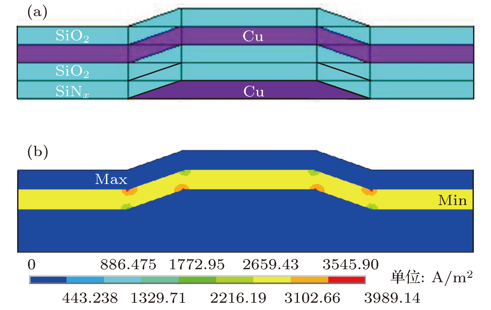
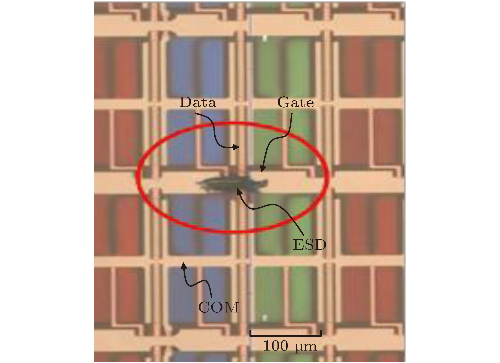
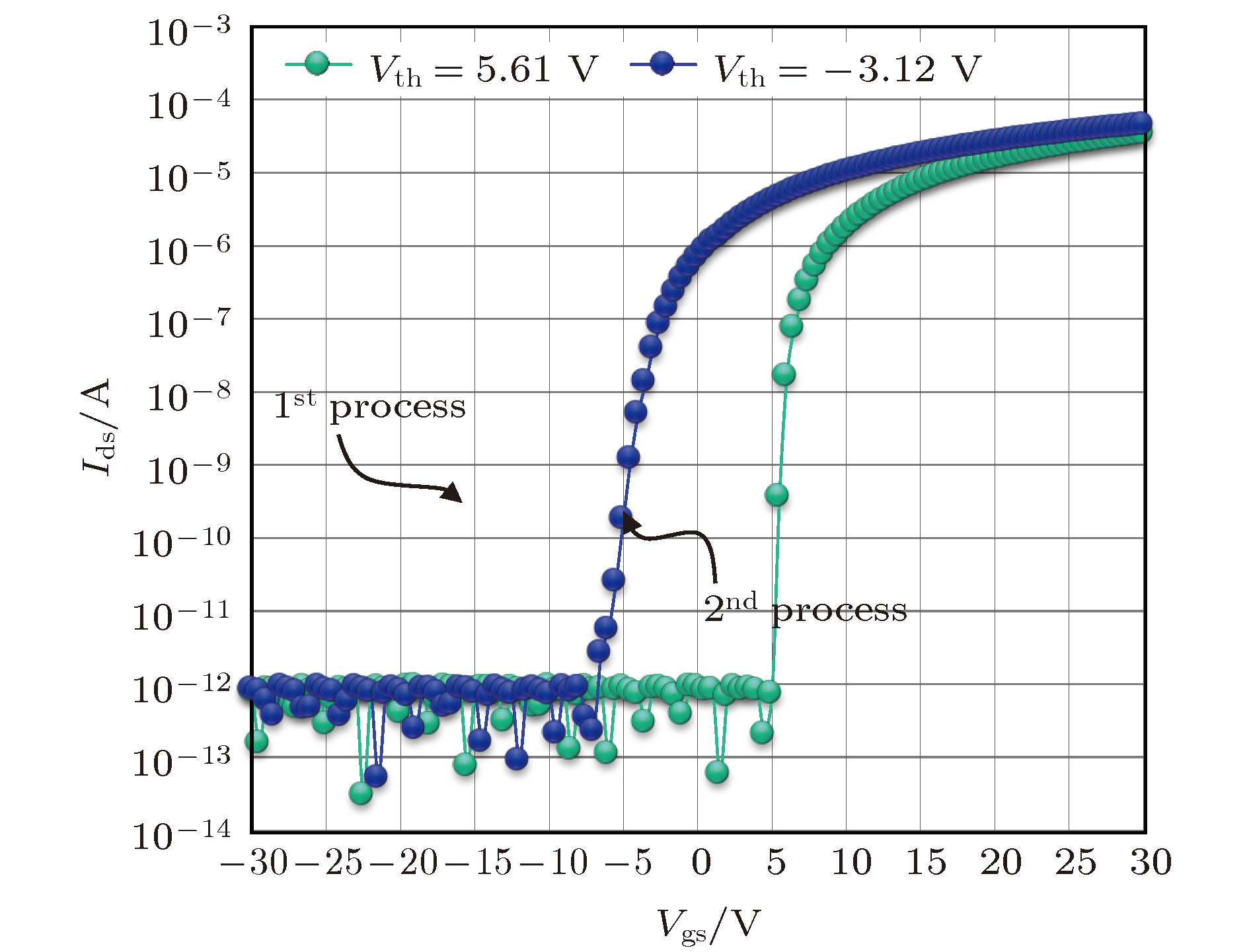
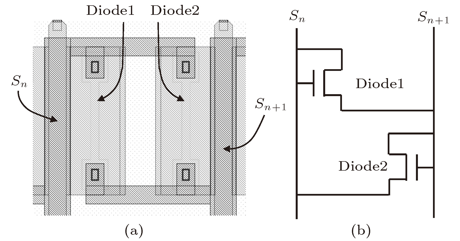
The InGaZnO thin film transistor (IGZO TFT) backplane combined with Cu interconnection has nearly an order of magnitude lower in the ability to withstand voltage than that of traditional a-Si TFT backplane on the production line. The breakdown voltage of Mo/Cu interconnection between data line and gate line is only about 60% of that of traditional a-Si TFT backplane. The electrostatic discharge (ESD) breakdown of Mo/Cu:SiNx/SiO2:Mo/Cu structure has become an important factor affecting the normal display of IGZO TFT ultra high definition (UHD) panel. We find that the anti-ESD damage ability of IGZO TFT devices needs matching with the anti-ESD damage ability of interlayer Cu interconnection in order to achieve a high-robustness IGZO TFT backplane. The position of ESD damage in IGZO TFT backplane is commonly in the climbing place where the data line crosses the scanning line. In this paper, a Cu diffusion model is proposed to explain the mechanism for the ESD failure of interlayer Cu interconnection. The Cu metal in gate line diffuses into SiNx/SiO2 gate insulator, and Cu metal at the corner of data line, where the date line crosses the gate line, diffuses into SiO2 film on the date line. The selection conditions of three kinds of protection architectures for ESD protection circuits around Cu interconnection, i.e. R-type, R-half-type, and Diode-type protection architectures, are proposed. On the basis of process optimization such as Cu metal film forming and Cu metal interface treatment, an ESD protection method for the Cu interconnection periphery of IGZO TFT backplane with high robustness is proposed. For the stable production process of IGZO TFT, combined with the design window of ESD protection circuit, the peripheral ESD protection circuit of Cu interconnect is designed with diode-type protection circuit on the IGZO TFT backplane of large-sized UHD and QUHD panel, which effectively improves the effect of interlayer Cu interconnection of IGZO TFT backplane on ESD damage. Through the production verification, it is proved that the metal diffusion of Cu interconnection on IGZO TFT backplane is the fundamental reason for reducing the anti-ESD damage ability of Mo/Cu:SiNx/SiO2:Mo/Cu structure. The rationality of the proposed ESD damage model for interlayer Cu interconnection is verified, which provides a theoretical basis for subsequent IGZO TFT backplane design with high robustness.
[1] 兰林锋, 张鹏, 彭俊彪 2016 65 128504
 Google Scholar
Lan L F, Zhang P, Peng J B 2016 Acta Phys. Sin. 65 128504
 Google Scholar
[2] Choi J H, Yang J H, Pi J E, Hwang C Y, Choi K, Kim H O, Kwon O S, Hwang C S 2017 IEEE Electron Dev. Lett. 38 1398
 Google Scholar
[3] Sang H L, Dong J O, Hwang A Y, Dong S H, Shin K, Jae K J, Jong W P 2015 IEEE Electron Dev. Lett. 36 802
 Google Scholar
[4] Nam W J, Shim J S, Shin H J, Kim J M, Ha W S, Park K H, Kim H G, Kim B S, Oh C H, Ahn B C, Kim B C, Cha S Y 2013 Sid Symposium Digest Technical Papers 44 243
[5] Lee C K, In D Y, Oh D J, Lee S H, Lee J W, Jeong J K 2018 IEEE Trans. Electron Dev. 65 1383
 Google Scholar
[6] Jeong J, Jun Lee G, Kim J, Choi B 2012 Appl. Phys. Lett. 100 112109
 Google Scholar
[7] Lee K W, Wang H, Bea J C, Murugesan M 2014 IEEE Electron Dev. Lett. 35 114
 Google Scholar
[8] 马群刚, 周刘飞, 喻玥, 马国永, 张盛东 2019 68 108501
 Google Scholar
Ma Q G, Zhou L F, Yu Y, Ma G Y, Zhang S D 2019 Acta Phys. Sin. 68 108501
 Google Scholar
[9] Liu X, Wang L L, Ning C, Hu H H, Yang W, Wang K, Yoo S Y, Zhang S D 2014 IEEE Trans. Electron Dev. 61 4299
 Google Scholar
[10] Ji K H, Kim J I, Jung H Y, Park S Y, Mo Y G, Jeong J K 2011 18th IEEE International Symposium on the Physical and Failure Analysis of Integrated Circuits (IPFA), Incheon, South Korea, July 4−7 2011, p12190972
[11] Simicic M, Hellings G, Chen S H, Myny K, Linten D 2018 40th Electrical Overstress/Electrostatic Discharge Symposium (EOS/ESD) Reno, NV, USA, September 23−28, 2018 p1
[12] Tai Y H, Chiu H L, Chou L S 2013 J. Disp. Technol. 9 613
 Google Scholar
[13] Liu Y, Chen R, Li B, En Y F, Chen Y Q 2017 IEEE Trans. Electron Dev. 65 356
 Google Scholar
[14] Scholz M, Steudel S, Myny K, Chen S, Boschke R, Hellings G, Linten D 2016 EOS/ESD Symp. Garden Grove, September 11−16, 2016 pp1−7
[15] Kim L Y, Kwon O K 2018 IEEE Electron Dev. Lett. 39 43
 Google Scholar
[16] Cao L, Ganesh K J, Zhang L, Aubel O, Hennesthal C, Hauschildt M, Ferreira P J, Ho P S 2013 Appl. Phys. Lett. 102 131907
[17] Hu C K, Gignac L M, Lian G, et al. 2018 IEEE International Electron Devices Meeting (IEDM) San Francisco, December 1−5, 2018 p18420793
[18] Chiang H C, Chang T C, Liao P Y, Chen B W, Tsao Y C, Tsai T M, Chien Y C, Yang Y C, Chen K F, Yang C I, Hung Y J, Chang K C, Zhang S D, Lin S C, Yeh C Y 2017 Appl. Phys. Lett. 111 133504
 Google Scholar
[19] Thermadam S P, Bhagat S K, Alford T L, Sakaguchi Y, Kozicki M N, Mitkova M 2010 Thin Solid Films 518 3293
 Google Scholar
[20] 邓小庆, 邓联文, 何伊妮, 廖聪维, 黄生祥, 罗衡 2019 68 057302
 Google Scholar
Deng X Q, Deng L W, He Y N, Liao C W, Huang S X, Luo H 2019 Acta Phys. Sin. 68 057302
 Google Scholar
[21] Chen W, Barnaby H J, Kozicki M N 2016 IEEE Electron Dev. Lett. 37 580
 Google Scholar
[22] Choi Z S, Mönig R, Thompson C V 2007 J. Appl. Phys. 102 083509
-
图 5 三种类型ESD保护电路的I-V曲线 (a) W = 5 μm, R型; (b) W = 4 μm, R型; (c) W = 5 μm, R half型; (d) W = 4 μm, R half型; (e) W = 5 μm, Diode型; (f) W = 4 μm, Diode型
Figure 5. Layout of three ESD protection architectures: (a) R-type I-V curves at W = 5 μm; (b) R-type I-V curves at W = 4 μm; (c) R half-type I-V curves at W = 5 μm; (d) R half-type I-V curves at W = 4 μm; (e) Diode-type I-V curves at W = 5 μm; (f) Diode-type I-V curves at W = 4 μm.
表 1 仿真模型中不同材料的属性参数
Table 1. Attribute parameters of different materials in simulation model.
材料 弹性模量/Pa 泊松比 热导率/W·mK–1 热膨胀系数/ppm·K–1 电阻率/Ω·m 质量密度/kg·m–3 SiO2 69 × 109 0.17 7.6 0.54 × 10⁻⁶ — 2200 Cu 119 × 109 0.326 398 17.5 × 10⁻⁶ 1.7 × 10⁻⁸ 8900 -
[1] 兰林锋, 张鹏, 彭俊彪 2016 65 128504
 Google Scholar
Lan L F, Zhang P, Peng J B 2016 Acta Phys. Sin. 65 128504
 Google Scholar
[2] Choi J H, Yang J H, Pi J E, Hwang C Y, Choi K, Kim H O, Kwon O S, Hwang C S 2017 IEEE Electron Dev. Lett. 38 1398
 Google Scholar
[3] Sang H L, Dong J O, Hwang A Y, Dong S H, Shin K, Jae K J, Jong W P 2015 IEEE Electron Dev. Lett. 36 802
 Google Scholar
[4] Nam W J, Shim J S, Shin H J, Kim J M, Ha W S, Park K H, Kim H G, Kim B S, Oh C H, Ahn B C, Kim B C, Cha S Y 2013 Sid Symposium Digest Technical Papers 44 243
[5] Lee C K, In D Y, Oh D J, Lee S H, Lee J W, Jeong J K 2018 IEEE Trans. Electron Dev. 65 1383
 Google Scholar
[6] Jeong J, Jun Lee G, Kim J, Choi B 2012 Appl. Phys. Lett. 100 112109
 Google Scholar
[7] Lee K W, Wang H, Bea J C, Murugesan M 2014 IEEE Electron Dev. Lett. 35 114
 Google Scholar
[8] 马群刚, 周刘飞, 喻玥, 马国永, 张盛东 2019 68 108501
 Google Scholar
Ma Q G, Zhou L F, Yu Y, Ma G Y, Zhang S D 2019 Acta Phys. Sin. 68 108501
 Google Scholar
[9] Liu X, Wang L L, Ning C, Hu H H, Yang W, Wang K, Yoo S Y, Zhang S D 2014 IEEE Trans. Electron Dev. 61 4299
 Google Scholar
[10] Ji K H, Kim J I, Jung H Y, Park S Y, Mo Y G, Jeong J K 2011 18th IEEE International Symposium on the Physical and Failure Analysis of Integrated Circuits (IPFA), Incheon, South Korea, July 4−7 2011, p12190972
[11] Simicic M, Hellings G, Chen S H, Myny K, Linten D 2018 40th Electrical Overstress/Electrostatic Discharge Symposium (EOS/ESD) Reno, NV, USA, September 23−28, 2018 p1
[12] Tai Y H, Chiu H L, Chou L S 2013 J. Disp. Technol. 9 613
 Google Scholar
[13] Liu Y, Chen R, Li B, En Y F, Chen Y Q 2017 IEEE Trans. Electron Dev. 65 356
 Google Scholar
[14] Scholz M, Steudel S, Myny K, Chen S, Boschke R, Hellings G, Linten D 2016 EOS/ESD Symp. Garden Grove, September 11−16, 2016 pp1−7
[15] Kim L Y, Kwon O K 2018 IEEE Electron Dev. Lett. 39 43
 Google Scholar
[16] Cao L, Ganesh K J, Zhang L, Aubel O, Hennesthal C, Hauschildt M, Ferreira P J, Ho P S 2013 Appl. Phys. Lett. 102 131907
[17] Hu C K, Gignac L M, Lian G, et al. 2018 IEEE International Electron Devices Meeting (IEDM) San Francisco, December 1−5, 2018 p18420793
[18] Chiang H C, Chang T C, Liao P Y, Chen B W, Tsao Y C, Tsai T M, Chien Y C, Yang Y C, Chen K F, Yang C I, Hung Y J, Chang K C, Zhang S D, Lin S C, Yeh C Y 2017 Appl. Phys. Lett. 111 133504
 Google Scholar
[19] Thermadam S P, Bhagat S K, Alford T L, Sakaguchi Y, Kozicki M N, Mitkova M 2010 Thin Solid Films 518 3293
 Google Scholar
[20] 邓小庆, 邓联文, 何伊妮, 廖聪维, 黄生祥, 罗衡 2019 68 057302
 Google Scholar
Deng X Q, Deng L W, He Y N, Liao C W, Huang S X, Luo H 2019 Acta Phys. Sin. 68 057302
 Google Scholar
[21] Chen W, Barnaby H J, Kozicki M N 2016 IEEE Electron Dev. Lett. 37 580
 Google Scholar
[22] Choi Z S, Mönig R, Thompson C V 2007 J. Appl. Phys. 102 083509
Catalog
Metrics
- Abstract views: 10968
- PDF Downloads: 160
- Cited By: 0


 DownLoad:


