


-
本文通过解析阵列基板栅极驱动(gate driver on array, GOA)电路中发生静电释放(electro-static discharge, ESD)的InGaZnO薄膜晶体管(InGaZnO thin-film transistor, IGZO TFT)器件发现:栅极Cu金属扩散进入了SiNx/SiO2栅极绝缘层; 源漏极金属层成膜前就发生了ESD破坏; 距离ESD破坏区域越近的IGZO TFT, 电流开关比越小, 直到源漏极与栅极完全短路. 本文综合IGZO TFT器件工艺、GOA区与显示区金属密度比、栅极金属层与绝缘层厚度非均匀性分布等因素, 采用ESD器件级分析与系统级分析相结合的方法, 提出栅极Cu:SiNx/SiO2界面缺陷以及这三层薄膜的厚度非均匀分布是导致GOA电路中沟道宽长比大的IGZO TFT发生ESD失效的关键因素, 并针对性地提出了改善方案.
-
关键词:
- Cu互连 /
- InGaZnO薄膜晶体管 /
- 阵列基板栅极驱动 /
- 静电释放
There is a risk of InGaZnO thin film transistor (IGZO TFT) failure, especially electro-static discharge (ESD) damage of gate driver on array (GOA) circuits, due to the combination of Cu interconnect, InGaZnO (IGZO) active layer and SiNx/SiO2 insulating layer used to realize large-scale ultra-high resolution display. It is found that the IGZO TFT damage position caused by ESD occurs between the source/drain metal layer and the gate insulator. The Cu metal of gate electrode diffuses into the gate insulator of SiNx/SiO2. The closer to the ESD damage area the IGZO TFT is, the more serious the negative bias of its threshold voltage (Vth) is until the device is fully turned on. The IGZO TFT with a large channel width-to-length ratio(W/L) in GOA circuit results in a serious negative bias of threshold voltage. In this paper, the ESD failure problem of GOA circuit in the IGZO TFT backplane is systematically analyzed by combining the ESD device level analysis with the system level analysis, which combines IGZO TFT device technology, difference in metal density between GOA region and active area on backplane, non-uniform thickness distribution of gate metal layer and gate insulator and so on. In the analysis of ESD device level, we propose that the diffusion of Cu metal from gate electrode into SiNx/SiO2 leads to the decrease of effective gate insulator layer, and that the built-in space charge effect leads to the decrease of the anti-ESD damage ability of IGZO TFT. In the analysis of ESD system level, we propose that the density of metal layers in GOA region is 4.5 times higher than that in active area of display panel, which makes the flatness of metal layer in GOA region worse. The non-uniformity of thickness of Cu metal film, SiNx film and SiO2 film around glass substrate lead to the position dependence of the anti-ESD damage ability of IGZO TFT in the GOA region. If there is a transition zone of film thickness change in IGZO TFT with large area, the ESD failure will occur easily. Accordingly, we propose to split large area IGZO TFT into several sub-TFT structures, which can effectively improve the ESD failure.-
Keywords:
- Cu interconnect /
- electrostatic-discharge /
- InGaZnO thin film transistor /
- gate driver on array
[1] Marko S, Geert H, Chen S H, Kris M, Dimitri L 2018 Electrical Overstress/electrostatic Discharge Symposium Reno, September 23-28, 2018 p1
[2] Liu Y, Chen R, Li B, En Y F, Chen Y Q 2017 IEEE Trans. Electron Dev. 1-5 99
[3] Tai Y H, Chiu H L, Chou L S 2013 J. Disp. Technol. 9 613
 Google Scholar
[4] Scholz M, Steudel S, Myny K, Chen S, Boschke R, Hellings G, Linten D 2016 Electrical Overstress/electrostatic Discharge Symposium Garden Grove, September 11-16, 2016 pp1-7.
[5] 宁洪龙, 胡诗犇, 朱峰, 姚日晖, 徐苗, 邹建华, 陶洪, 徐瑞霞, 徐华, 王磊, 兰林锋, 彭俊彪 2015 64 126103
Google Scholar
Ning H L, Hu S B, Zhu F, Yao R H, Xu M, Zou J H, Tao H, Xu R X, Xu H, Wang L, Lan L F, Peng J B 2015 Acta Phys. Sin. 64 126103
Google Scholar
[6] Kim L Y, Kwon O K 2018 IEEE Electr. Device Lett. 39 43
Google Scholar
[7] Lin C L, Wu C E, Chen F H, Lai P C, Cheng M H 2016 IEEE Trans. Electron Dev. 63 2405
Google Scholar
[8] Geng D, Chen Y F, Mativenga M, Jin J 2015 IEEE Electr. Device Lett. 36 805
Google Scholar
[9] Chen W, Barnaby H J, Kozicki M N 2016 IEEE Electr. Device Lett. 37 580
Google Scholar
[10] Choi Z S, Mönig R, Thompson C V 2007 J. Appl. Phys. 102 387
[11] Lee K W, Wang H, Bea J C, Murugesan M 2014 IEEE Electr. Device Lett. 35 114
Google Scholar
[12] Xiang L, Wang L L, Ning C, Hu H, Wei Y, Wang K, Yoo S Y, Zhang S D 2014 IEEE Trans. Electron Dev. 61 4299
Google Scholar
[13] Han K L, Ok K C, Cho H S, Oh S, Park J S 2017 Appl. Phys. Lett. 111 063502
Google Scholar
[14] Tari A, Lee C H, Wong W S 2015 Appl. Phys. Lett. 107 1679
[15] Hung S C, Chiang C H, Li Y M 2015 J. Display Tech. 11 640
Google Scholar
[16] Hu C K, Gignac L M, Lian G 2018 IEEE International Electron Devices Meeting (IEDM) San Francisco, December 1-5, 2018
[17] Thermadam S P, Bhagat S K, Alford T L, Sakaguchi Y, Kozicki M N, Mitkova M 2010 Thin Solid Films 518 3293
Google Scholar
[18] Toumi S, Ouennoughi Z, Strenger K C 2016 Solid State Electron. 122 56
Google Scholar
[19] Christen T 2017 IEEE T. Dielect. E. I. 23 3712
[20] Choi S, Jang J, Kang H, Baeck J H, Bae J U, Park K S, Yoon S Y, Kang I B, Kim D M, Choi S J, Kim Y S, Oh S, Kim D H 2017 IEEE Electr. Device Lett. 38 580
Google Scholar
[21] Jang J, Kim D G, Kim D M, Choi S J, Kim D H 2014 Appl. Phys. Lett. 105 1117
[22] 强蕾, 姚若河 2012 61 087303
Google Scholar
Qiang L, Yao R H 2012 Acta Phys. Sin. 61 087303
Google Scholar
[23] 邓小庆, 邓联文, 何伊妮, 廖聪维, 黄生祥, 罗衡 2019 68 057302
Deng X Q, Deng L W, He Y N, Liao C W, Huang S X, Luo H 2019 Acta Phys. Sin. 68 057302
[24] Wang W, Xu G W, Chowdhury M D H, Wang H, Um J K, Ji Z Y, Gao N, Zong Z W, Bi C, Lu C Y, Lu N D, Banerjee W, Feng J F, Li L, Kadashchuk A, Jang J, Liu M 2018 Phys. Rev. B 98 245
-

图 1 13T1C架构的GOA电路单元原理图
Fig. 1. Diagram of the GOA circuit unit composed of 13 TFTs and 1 capacitor.
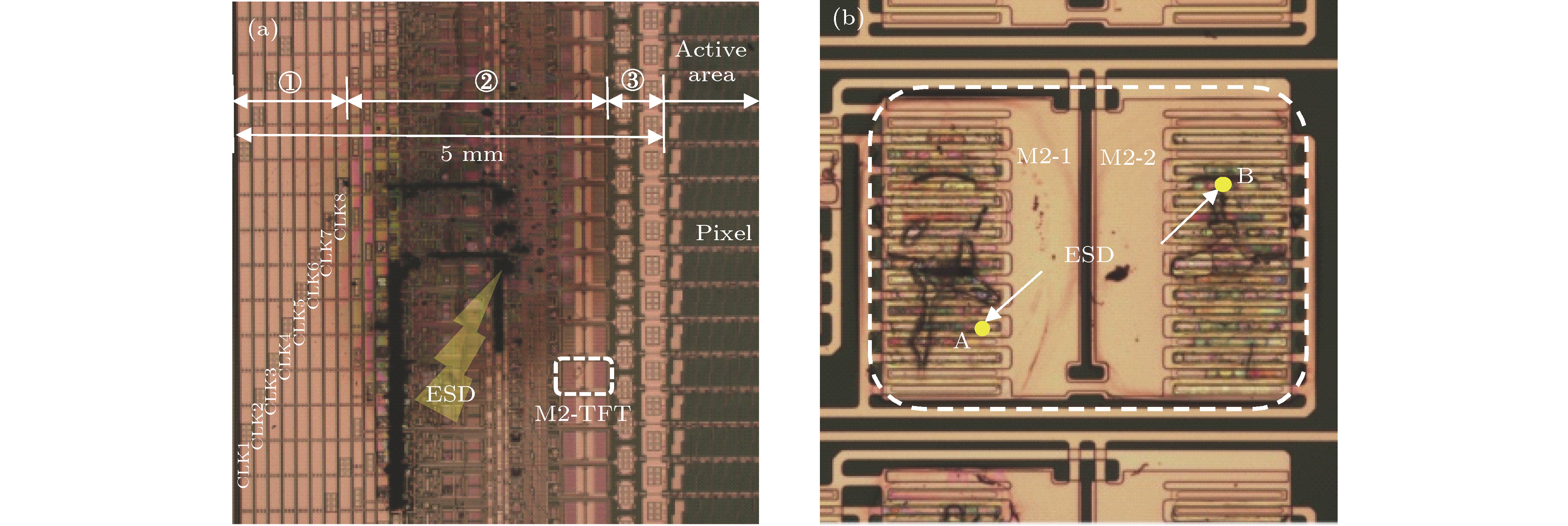
图 2 GOA电路的ESD破坏现象 (a) GOA区大面积的ESD烧伤现象; (b) M2 TFT的ESD破坏现象
Fig. 2. ESD damage phenomenon of GOA circuit: (a) Photo image of the overall GOA where ESD damage occurs. (b) photo image of ESD damage M2 TFT in the GOA unit.
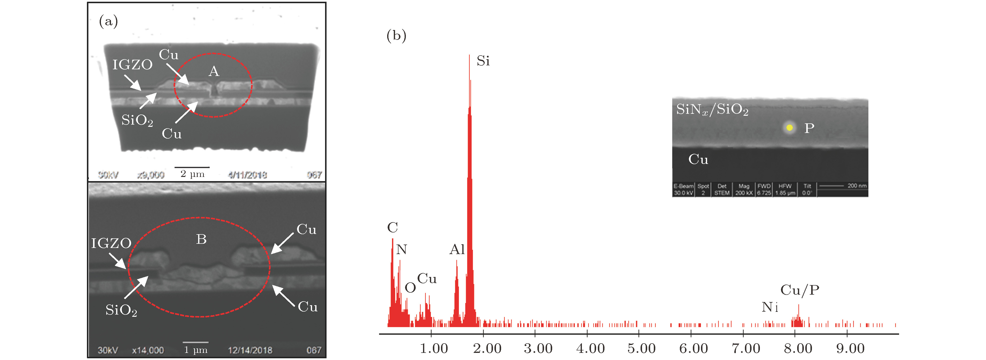
图 3 M2 TFT的ESD失效区域解析 (a) ESD失效位置的FIB断面解析; (b) ESD失效位置的栅极绝缘层元素分析
Fig. 3. Analysis of ESD failure area of M2 TFT: (a) FIB section analysis of ESD failure position; (b) elemental analysis of gate insulator at failure position of ESD.
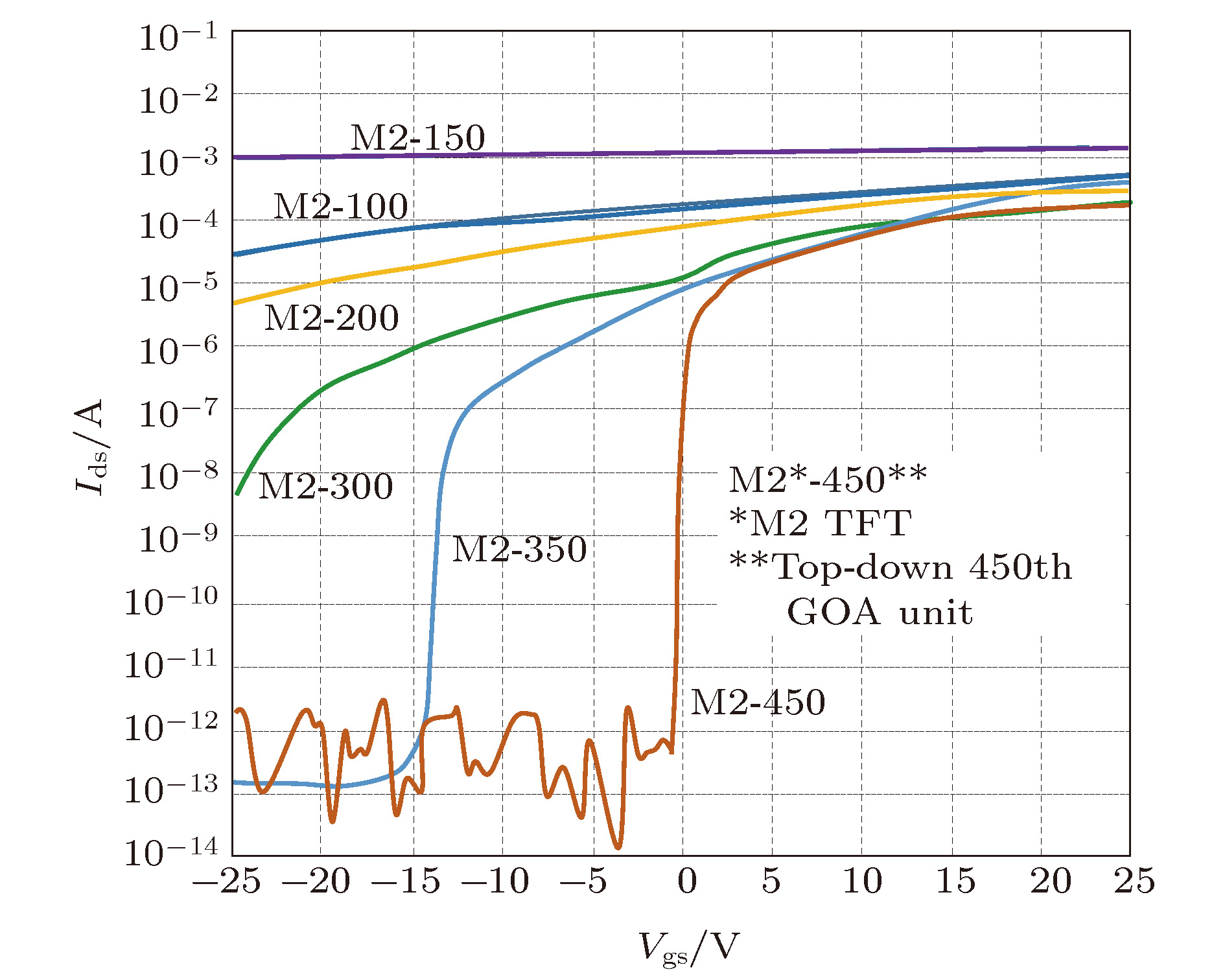
图 4 距离ESD失效中心不同位置的M2 TFT特性
Fig. 4. M2 TFT characteristics at different positions from ESD failure center.

图 5 Cu扩散引起的空间电荷效应与ESD失效机理
Fig. 5. Mechanism of space charge effect formed by Cu2+ ion entering SiO2.

图 6 Cu:SiNx/SiO2三层薄膜的厚度等值线分布
Fig. 6. Thickness contour distribution of Cu: SiNx/SiO2 three films.
表 1 GOA区M2 TFT不同设计方案比较
Table 1. Comparison of different design schemes of M2 TFT in GOA.
结构 2个子TFT 6个子TFT 8个子TFT 版图 
版图空间 274.5 μm × 259.2 μm 274.5 μm × 300.2 μm 274.5 μm × 351.2 μm 扫描线面积 53158.8 59647.3 65519.6 数据线面积 43155.8 46190.2 49248.2 扫描线密度 74.71% 72.4% 68% 数据线密度 60.7% 56.1% 51.1%  下载: 导出CSV
-
[1] Marko S, Geert H, Chen S H, Kris M, Dimitri L 2018 Electrical Overstress/electrostatic Discharge Symposium Reno, September 23-28, 2018 p1
[2] Liu Y, Chen R, Li B, En Y F, Chen Y Q 2017 IEEE Trans. Electron Dev. 1-5 99
[3] Tai Y H, Chiu H L, Chou L S 2013 J. Disp. Technol. 9 613
Google Scholar
[4] Scholz M, Steudel S, Myny K, Chen S, Boschke R, Hellings G, Linten D 2016 Electrical Overstress/electrostatic Discharge Symposium Garden Grove, September 11-16, 2016 pp1-7.
[5] 宁洪龙, 胡诗犇, 朱峰, 姚日晖, 徐苗, 邹建华, 陶洪, 徐瑞霞, 徐华, 王磊, 兰林锋, 彭俊彪 2015 64 126103
Google Scholar
Ning H L, Hu S B, Zhu F, Yao R H, Xu M, Zou J H, Tao H, Xu R X, Xu H, Wang L, Lan L F, Peng J B 2015 Acta Phys. Sin. 64 126103
Google Scholar
[6] Kim L Y, Kwon O K 2018 IEEE Electr. Device Lett. 39 43
Google Scholar
[7] Lin C L, Wu C E, Chen F H, Lai P C, Cheng M H 2016 IEEE Trans. Electron Dev. 63 2405
Google Scholar
[8] Geng D, Chen Y F, Mativenga M, Jin J 2015 IEEE Electr. Device Lett. 36 805
Google Scholar
[9] Chen W, Barnaby H J, Kozicki M N 2016 IEEE Electr. Device Lett. 37 580
Google Scholar
[10] Choi Z S, Mönig R, Thompson C V 2007 J. Appl. Phys. 102 387
[11] Lee K W, Wang H, Bea J C, Murugesan M 2014 IEEE Electr. Device Lett. 35 114
Google Scholar
[12] Xiang L, Wang L L, Ning C, Hu H, Wei Y, Wang K, Yoo S Y, Zhang S D 2014 IEEE Trans. Electron Dev. 61 4299
Google Scholar
[13] Han K L, Ok K C, Cho H S, Oh S, Park J S 2017 Appl. Phys. Lett. 111 063502
Google Scholar
[14] Tari A, Lee C H, Wong W S 2015 Appl. Phys. Lett. 107 1679
[15] Hung S C, Chiang C H, Li Y M 2015 J. Display Tech. 11 640
Google Scholar
[16] Hu C K, Gignac L M, Lian G 2018 IEEE International Electron Devices Meeting (IEDM) San Francisco, December 1-5, 2018
[17] Thermadam S P, Bhagat S K, Alford T L, Sakaguchi Y, Kozicki M N, Mitkova M 2010 Thin Solid Films 518 3293
Google Scholar
[18] Toumi S, Ouennoughi Z, Strenger K C 2016 Solid State Electron. 122 56
Google Scholar
[19] Christen T 2017 IEEE T. Dielect. E. I. 23 3712
[20] Choi S, Jang J, Kang H, Baeck J H, Bae J U, Park K S, Yoon S Y, Kang I B, Kim D M, Choi S J, Kim Y S, Oh S, Kim D H 2017 IEEE Electr. Device Lett. 38 580
Google Scholar
[21] Jang J, Kim D G, Kim D M, Choi S J, Kim D H 2014 Appl. Phys. Lett. 105 1117
[22] 强蕾, 姚若河 2012 61 087303
Google Scholar
Qiang L, Yao R H 2012 Acta Phys. Sin. 61 087303
Google Scholar
[23] 邓小庆, 邓联文, 何伊妮, 廖聪维, 黄生祥, 罗衡 2019 68 057302
Deng X Q, Deng L W, He Y N, Liao C W, Huang S X, Luo H 2019 Acta Phys. Sin. 68 057302
[24] Wang W, Xu G W, Chowdhury M D H, Wang H, Um J K, Ji Z Y, Gao N, Zong Z W, Bi C, Lu C Y, Lu N D, Banerjee W, Feng J F, Li L, Kadashchuk A, Jang J, Liu M 2018 Phys. Rev. B 98 245


 下载:
下载:


计量
- 文章访问数: 13353
- PDF下载量: 185
- 被引次数: 0
