


-
In this paper, a Ni/Au vertical structure Schottky diode based on mechanically exfoliated β-Ga2O3 is fabricated. The temperature dependent characteristics of I-V curves are measured. The device shows a good rectifying behavior. As the temperature increases from 300 K to 473 K, the barrier height increases from 1.08 eV to 1.35 eV, and the ideal factor decreases from 1.32 to 1.19. Both of them show strong temperature dependence, which indicates that the Schottky barrier of the device is inhomogeneous. The device has a double exponential forward I-V characteristic curve, which may be related to crystal defects, surface states, surface energy band bending and the effect of mechanical exfoliation from the crystal surface. Through Cheung's method and Norde's method, the series resistances and barrier heights of the device at different temperatures are extracted. It is found that the parameters extracted by the Norde's method are in good agreement with the values obtained from the forward I-V curve. The series resistance decreases with temperature increasing, which is mainly caused by the increase of the concentration of thermally excited carriers. In this paper, the temperature characteristics of the device are modified by the Gauss distribution of the barrier height. The corrected barrier height is 1.54 eV and Richardson's constant is 26.35 A·cm–2·K–2, which is closer to the theoretical value. It shows that the I-V temperature characteristics of Au/Ni/β-Ga2O3 Schottky diodes can be described by the thermionic emission model of the Gauss distribution barrier height accurately. There are a lot of surface states on the surface of Ga2O3 single crystal obtained by Mechanical exfoliation, which has a great influence on the Schottky contact of the device and may lead to the inhomogeneity of Schottky barriers. At the same time, due to mechanical exploiation, the surface of gallium oxide single crystal material is not completely continuous, and the single crystal surface has layered or island structure. This will also cause the inhomogeneous Schottky barrier height. Considering the influence of inhomogeneous barrier on Schottky diode, the method of measuring the temperature characteristics is more suitable to extracting the electrical parameters of β-Ga2O3 Schottky diodes than the method of fitting I-V forward curve by TE model.
-
Keywords:
- Gallium oxide /
- mechanically exfoliated /
- Schottky diode /
- temperature dependent characteristic
[1] 郭道友, 李培刚, 陈政委, 吴真平, 唐为华 2019 68 078501
 Google Scholar
Guo D Y, Li P G, Chen Z W, Wu Z P, Tang W H 2019 Acta Phys. Sin. 68 078501
Google Scholar
[2] Montes J, Yang C, Fu H, Yang T H, Fu K, Chen H, Zhou J, Huang X, Zhao Y 2019 Appl. Phys. Lett. 114 162103
Google Scholar
[3] Barman S K, Huda M N 2019 Phys. Status Solidi-R. 13 1800554
Google Scholar
[4] Qian L X, Wang Y, Wu Z H, Sheng T, Liu X Z 2017 Vacuum 140 106
Google Scholar
[5] Wang X, Liu Z, Zhi Y, Li S, Wu Z, Li P, Tang W 2019 Vacuum 166 79
Google Scholar
[6] Manandhar S, Battu A K, Devaraj A, Shutthanandan V, Thevuthasan S, Ramana C V 2020 Sci. Rep. 10 178
Google Scholar
[7] Yang J, Ren F, Tadjer M, Pearton S, Kuramata A 2018 ECS J. Solid State Sc. 7 Q92
Google Scholar
[8] Galazka Z, Irmscher K, Schewski R, Hanke I M, Pietsch M, Ganschow S, Klimm D, Dittmar A, Fiedler A, Schroeder T, Bickermann M 2020 J. Cryst. Growth 529 Unsp 125297
[9] Tang H L, He N T, Zhang H, Liu B, Zhu Z C, Xu M X, Chen L, Liu J L, Ouyang X P, Xu J 2020 Crystengcomm 22 924
Google Scholar
[10] Matsuzaki K, Hiramatsu H, Nomura K, Yanagi H, Kamiya T, Hirano M, Hosono H 2006 Thin Solid Films 496 37
Google Scholar
[11] Wang D, He L N, Le Y, Feng X J, Luan C N, Xiao H D, Ma J 2020 Ceram. Int. 46 4568
Google Scholar
[12] Matsuzaki K, Yanagi H, Kamiya T, Hiramatsu H, Nomura K, Hirano M, Hosono H 2006 Appl. Phys. Lett. 88 92106
Google Scholar
[13] Orita M, Ohta H, Hirano M, Hosono H 2000 Appl. Phys. Lett. 77 4166
Google Scholar
[14] Konishi K, Goto K, Murakami H, Kumagai Y, Higashiwaki M 2017 Appl. Phys. Lett. 110 103506
Google Scholar
[15] Pearton S J, Ren F, Tadjer M, Kim J 2018 J. Appl. Phys. 124 220901
Google Scholar
[16] Yao Y, Gangireddy R, Kim J, Das K K, Porter L M 2017 J. Vac. Sci. Technol., B 35 03D113
Google Scholar
[17] Cheung S K, Cheung N W 1986 Appl. Phys. Lett. 49 85
Google Scholar
[18] Norde H 1979 J. Appl. Phys. 50 5052
Google Scholar
[19] He Q, Mu W, Dong H, Long S, Jia Z, Lv H, Liu Q, Tang M, Tao X, Liu M 2017 Appl. Phys. Lett. 110 093503
Google Scholar
[20] Ahn S, Ren F, Yuan L, Pearton S J, Kuramata A 2017 ECS J. Solid State Sc. 6 P68
Google Scholar
[21] Jian G, He Q, Mu W, Fu B, Dong H, Qin Y, Zhang Y, Xue H, Long S, Jia Z, Lv H, Liu Q, Tao X, Liu M 2018 AIP Adv. 8 015316
Google Scholar
[22] Fares C, Ren F, Pearton S J 2018 ECS J. Solid State Sc. 8 Q3007
Google Scholar
[23] Reddy P R S, Janardhanam V, Shim K H, Reddy V R, Lee S N, Park S J, Choi C J 2020 Vacuum 171 109012
Google Scholar
[24] 施敏, 伍国珏(耿莉, 张瑞智译) 2008 半导体器件物理(第3版) (西安: 西安交通大学出版社) 第118−119页
Sze S M, Kwok K N (translated by Geng L, Zhang R) 2008 Physics of Semiconductor Devices (3rd Ed.) (Xi'an: Xi'an Jiaotong University Press) pp118−119 (in Chinese)
[25] Shi J J, Xia X C, Liang H W, Abbas Q, Liu J, Zhang H Q, Liu Y 2019 J. Mater. Sci.-Mater. Electron. 30 3860
Google Scholar
[26] Ohdomari I, Tu K N 1980 J. Appl. Phys. 51 3735
Google Scholar
[27] Tung R T 1992 Phys. Rev. B 45 13509
Google Scholar
[28] Güçlü Ç Ş, Özdemir A F, Altindal Ş 2016 Appl. Phys. A 122 1032.1
Google Scholar
[29] Marıl E, Altındal Ş, Kaya A, Koçyiğit S, Uslu İ 2015 Philos. Mag. 95 1049
Google Scholar
[30] Garrido-Alzar C L 1997 Renewable Energy 10 4
Google Scholar
[31] Janardhanam V, Jyothi I, Sekhar Reddy P R, Cho J, Cho J M, Choi C J, Lee S N, Rajagopal Reddy V 2018 Superlattices Microstruct. 120 508
Google Scholar
[32] Jyothi I, Seo M W, Janardhanam V, Shim K H, Lee Y B, Ahn K S, Choi C J 2013 J. Alloys Compd. 556 252
Google Scholar
[33] Mönch W 2007 Appl. Phys. A 87 359
Google Scholar
[34] Li A, Feng Q, Zhang J, Hu Z, Feng Z, Zhang K, Zhang C, Zhou H, hao Y 2018 Superlattices Microstruct. 119 212
Google Scholar
[35] Shen Y, Feng Q, Zhang K, Hu Z, Yan G, Cai Y, Mu W, Jia Z, Zhang C, Zhou H, Zhang J, Lian X, Lai Z, Hao Y 2019 Superlattices Microstruct. 133 106179
Google Scholar
[36] 施敏, 伍国珏 (耿莉, 张瑞智译) 2008 半导体器件物理 (第3版) (西安: 西安交通大学出版社) 第132−133页
Sze S M, Kwok K N (translated by Geng L, Zhang R) 2008 Physics of Semiconductor Devices (3rd Ed.) (Xi'an: Xi'an Jiaotong University Press) pp132−133 (in Chinese)
[37] Sasaki K, Higashiwaki M, Kuramata A, Masui T, Yamakoshi S 2013 IEEE Electron Device Lett. 34 493
Google Scholar
[38] Werner J H, Güttler H H 1991 J. Appl. Phys. 69 1522
Google Scholar
-
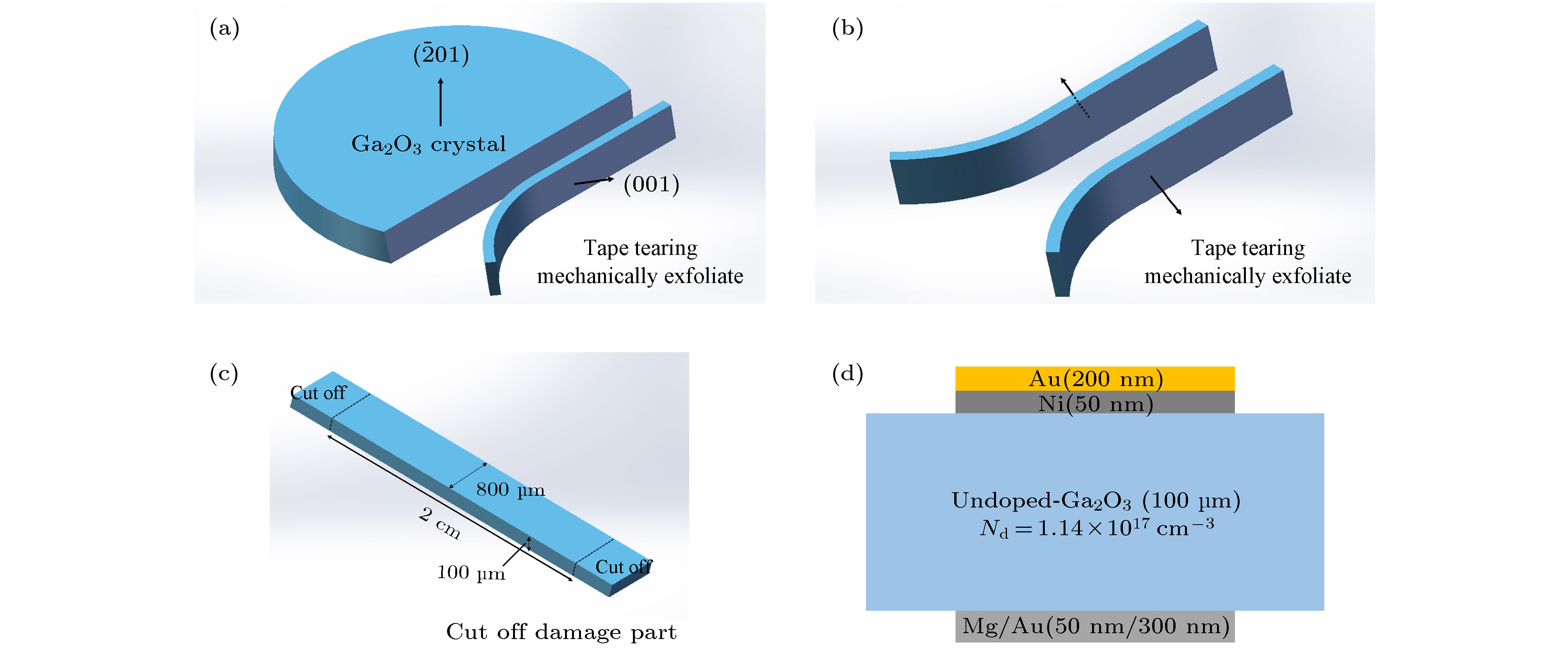
图 1 (a), (b), (c) 机械剥离氧化镓单晶材料; (d) Au/Ni/β-Ga2O3肖特基二极管结构示意图
Figure 1. (a), (b), (c) Mechanically exfoliated beta-Ga2O3 single crystal; (d) schematic cross section of Au/Ni/β-Ga2O3 Schottky barrier diode.
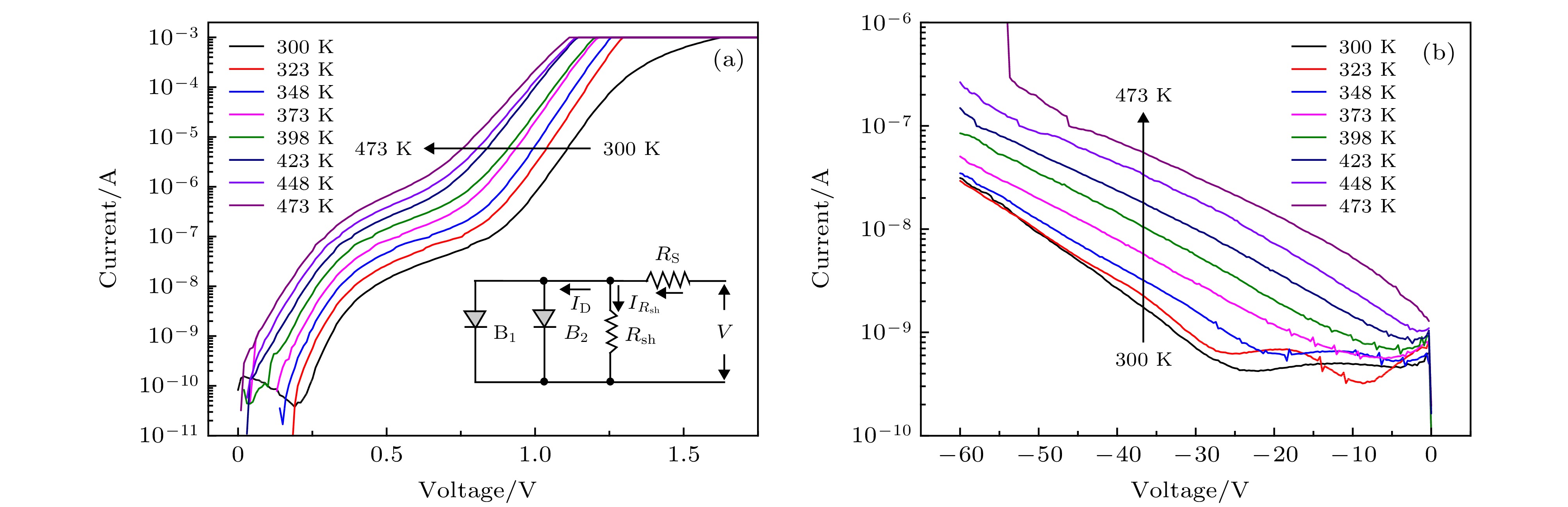
图 2 肖特基二极管的I-V温度特性曲线 (a) 正向; (b) 反向
Figure 2. Temperature dependent I-V characteristic curves of Schottky barrier diode: (a) Forward curves; (b) reverse curves.

图 3 I-V温度特性曲线提取的 (a) 势垒高度; (b) 理想因子; (c) 阈值电压
Figure 3. The parameters from temperature dependent I-V characteristic curves: (a)Barrier height; (b) ideal factor; (c) threshold voltage.

图 4 不同温度下势垒高度与理想因子依赖关系 (a) Barrier 1; (b) Barrier 2
Figure 4. Plot of barrier height as a function of ideal factor obtained at various temperatures: (a) Barrier 1; (b) Barrier 2

图 5 (a) C-V特性曲线; (b) 频率为100 kHz的1/C 2-V曲线
Figure 5. (a) C-V characteristic curves; (b) 1/C 2-V characteristic curve of 100 kHz.

图 6 300 K温度下的dV/dlnI-V曲线
Figure 6. dV/dlnI-V curve at the temperature of 300 K.
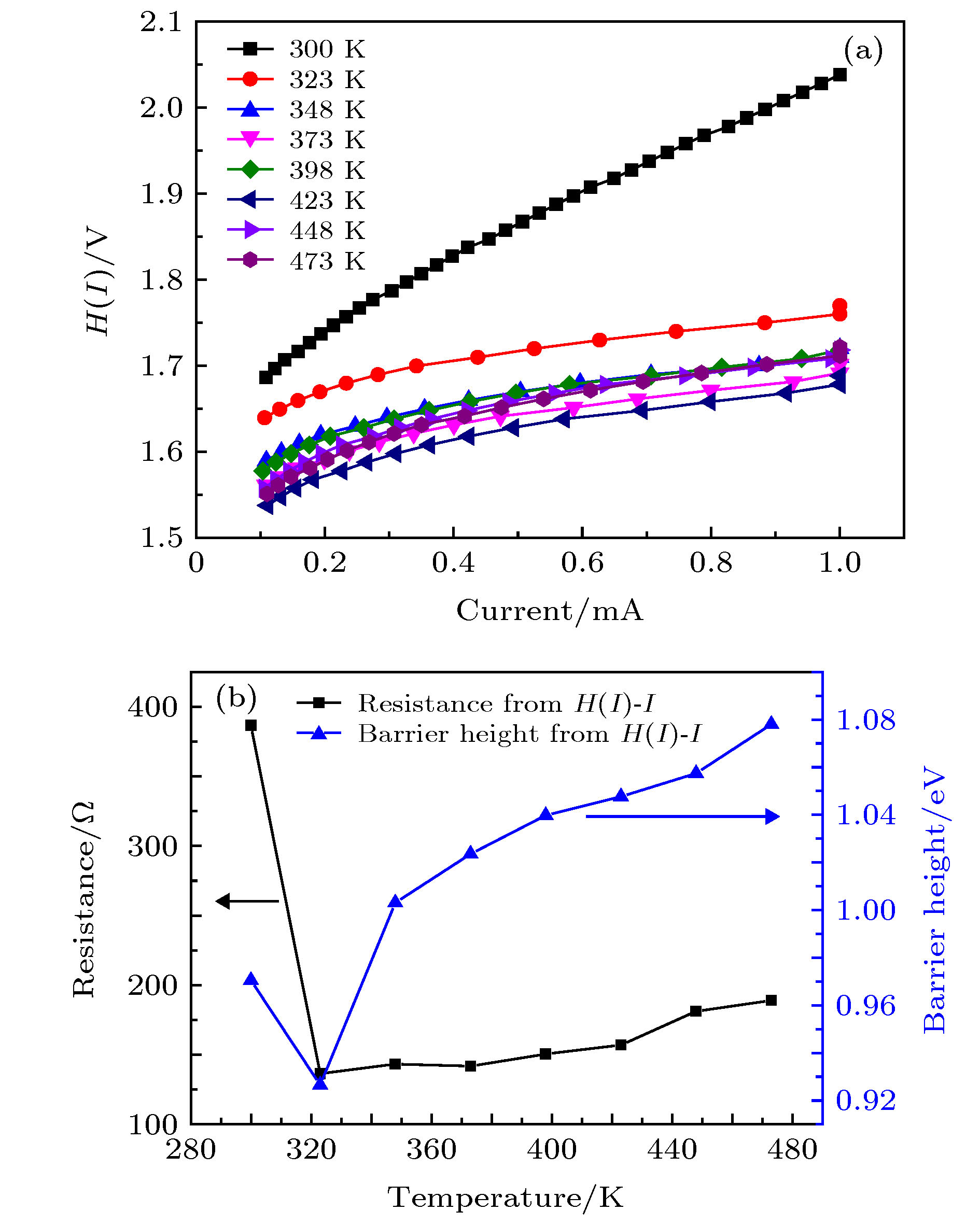
图 7 H(I)-I (a) 温度特性曲线; (b) 不同温度时的串联电阻和势垒高度
Figure 7. H(I)-I (a) Temperature dependent curves; (b) the resistance and barrier height at various temperatures.

图 8 (a) F(V)-V 温度特性曲线; (b) 不同温度时的串联电阻和势垒高度
Figure 8. (a) F(V)-V temperature dependent curves; (b) the resistance and barrier height at various temperatures.
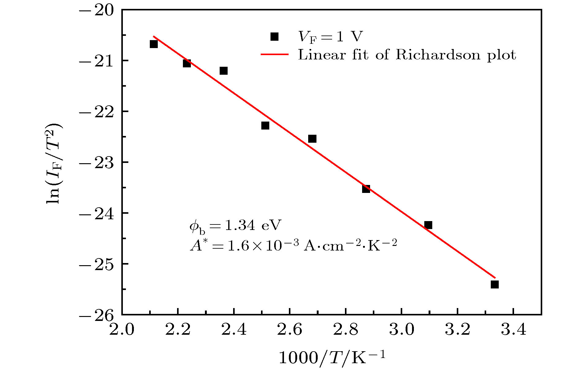
图 9 肖特基二极管的理查孙图
Figure 9. Richardson's plot of Schottky barrier diode.

图 10 (a)
$ {\varphi }_{{\rm{a}}{\rm{p}}} -\dfrac{1}{2 kT} $ 图像; (b) 高斯分布修正后的理查孙图Figure 10. (a) The plot of
$ {\varphi }_{{\rm{a}}{\rm{p}}} - \dfrac{1}{2 kT} $ ; (b) Richardson's plot after Gaussian distribution processing.表 1 I-V温度特性曲线提取数据表
Table 1. The parameters from temperature dependent I-V characteristic curves.
温度/K 势垒高度/eV 理想因子n 阈值电压/V Barrier 1 Barrier 2 Barrier 1 Barrier 2 Barrier 1 Barrier 2 300 1.01 1.08 1.32 2.11 1.02 1.77 323 1.00 1.17 1.74 1.81 1.28 1.64 348 1.08 1.23 1.46 1.71 1.16 1.61 373 1.13 1.25 1.36 1.69 1.11 1.58 398 1.17 1.29 1.37 1.67 1.14 1.59 423 1.22 1.30 1.28 1.65 1.10 1.56 448 1.27 1.32 1.24 1.71 1.09 1.59 473 1.31 1.35 1.19 1.69 1.06 1.58  DownLoad: CSV
表 2 H(I)-I与F(V)-V曲线提取数据表
Table 2. The parameters from H(I)-I curves and F(V)-V curves.
温度/K 势垒高度/eV 串联电阻/Ω H(I)-I F(V)-V H(I)-I F(V)-V 300 0.97 1.07 386.62 12299.25 323 0.93 1.10 136.38 6184.64 348 1.00 1.15 143.32 3086.28 373 1.02 1.19 141.79 1603.53 398 1.04 1.23 150.50 838.20 423 1.05 1.27 157.03 379.21 448 1.06 1.29 181.14 381.55 473 1.08 1.34 189.04 157.33
DownLoad: CSV
-
[1] 郭道友, 李培刚, 陈政委, 吴真平, 唐为华 2019 68 078501
Google Scholar
Guo D Y, Li P G, Chen Z W, Wu Z P, Tang W H 2019 Acta Phys. Sin. 68 078501
Google Scholar
[2] Montes J, Yang C, Fu H, Yang T H, Fu K, Chen H, Zhou J, Huang X, Zhao Y 2019 Appl. Phys. Lett. 114 162103
Google Scholar
[3] Barman S K, Huda M N 2019 Phys. Status Solidi-R. 13 1800554
Google Scholar
[4] Qian L X, Wang Y, Wu Z H, Sheng T, Liu X Z 2017 Vacuum 140 106
Google Scholar
[5] Wang X, Liu Z, Zhi Y, Li S, Wu Z, Li P, Tang W 2019 Vacuum 166 79
Google Scholar
[6] Manandhar S, Battu A K, Devaraj A, Shutthanandan V, Thevuthasan S, Ramana C V 2020 Sci. Rep. 10 178
Google Scholar
[7] Yang J, Ren F, Tadjer M, Pearton S, Kuramata A 2018 ECS J. Solid State Sc. 7 Q92
Google Scholar
[8] Galazka Z, Irmscher K, Schewski R, Hanke I M, Pietsch M, Ganschow S, Klimm D, Dittmar A, Fiedler A, Schroeder T, Bickermann M 2020 J. Cryst. Growth 529 Unsp 125297
[9] Tang H L, He N T, Zhang H, Liu B, Zhu Z C, Xu M X, Chen L, Liu J L, Ouyang X P, Xu J 2020 Crystengcomm 22 924
Google Scholar
[10] Matsuzaki K, Hiramatsu H, Nomura K, Yanagi H, Kamiya T, Hirano M, Hosono H 2006 Thin Solid Films 496 37
Google Scholar
[11] Wang D, He L N, Le Y, Feng X J, Luan C N, Xiao H D, Ma J 2020 Ceram. Int. 46 4568
Google Scholar
[12] Matsuzaki K, Yanagi H, Kamiya T, Hiramatsu H, Nomura K, Hirano M, Hosono H 2006 Appl. Phys. Lett. 88 92106
Google Scholar
[13] Orita M, Ohta H, Hirano M, Hosono H 2000 Appl. Phys. Lett. 77 4166
Google Scholar
[14] Konishi K, Goto K, Murakami H, Kumagai Y, Higashiwaki M 2017 Appl. Phys. Lett. 110 103506
Google Scholar
[15] Pearton S J, Ren F, Tadjer M, Kim J 2018 J. Appl. Phys. 124 220901
Google Scholar
[16] Yao Y, Gangireddy R, Kim J, Das K K, Porter L M 2017 J. Vac. Sci. Technol., B 35 03D113
Google Scholar
[17] Cheung S K, Cheung N W 1986 Appl. Phys. Lett. 49 85
Google Scholar
[18] Norde H 1979 J. Appl. Phys. 50 5052
Google Scholar
[19] He Q, Mu W, Dong H, Long S, Jia Z, Lv H, Liu Q, Tang M, Tao X, Liu M 2017 Appl. Phys. Lett. 110 093503
Google Scholar
[20] Ahn S, Ren F, Yuan L, Pearton S J, Kuramata A 2017 ECS J. Solid State Sc. 6 P68
Google Scholar
[21] Jian G, He Q, Mu W, Fu B, Dong H, Qin Y, Zhang Y, Xue H, Long S, Jia Z, Lv H, Liu Q, Tao X, Liu M 2018 AIP Adv. 8 015316
Google Scholar
[22] Fares C, Ren F, Pearton S J 2018 ECS J. Solid State Sc. 8 Q3007
Google Scholar
[23] Reddy P R S, Janardhanam V, Shim K H, Reddy V R, Lee S N, Park S J, Choi C J 2020 Vacuum 171 109012
Google Scholar
[24] 施敏, 伍国珏(耿莉, 张瑞智译) 2008 半导体器件物理(第3版) (西安: 西安交通大学出版社) 第118−119页
Sze S M, Kwok K N (translated by Geng L, Zhang R) 2008 Physics of Semiconductor Devices (3rd Ed.) (Xi'an: Xi'an Jiaotong University Press) pp118−119 (in Chinese)
[25] Shi J J, Xia X C, Liang H W, Abbas Q, Liu J, Zhang H Q, Liu Y 2019 J. Mater. Sci.-Mater. Electron. 30 3860
Google Scholar
[26] Ohdomari I, Tu K N 1980 J. Appl. Phys. 51 3735
Google Scholar
[27] Tung R T 1992 Phys. Rev. B 45 13509
Google Scholar
[28] Güçlü Ç Ş, Özdemir A F, Altindal Ş 2016 Appl. Phys. A 122 1032.1
Google Scholar
[29] Marıl E, Altındal Ş, Kaya A, Koçyiğit S, Uslu İ 2015 Philos. Mag. 95 1049
Google Scholar
[30] Garrido-Alzar C L 1997 Renewable Energy 10 4
Google Scholar
[31] Janardhanam V, Jyothi I, Sekhar Reddy P R, Cho J, Cho J M, Choi C J, Lee S N, Rajagopal Reddy V 2018 Superlattices Microstruct. 120 508
Google Scholar
[32] Jyothi I, Seo M W, Janardhanam V, Shim K H, Lee Y B, Ahn K S, Choi C J 2013 J. Alloys Compd. 556 252
Google Scholar
[33] Mönch W 2007 Appl. Phys. A 87 359
Google Scholar
[34] Li A, Feng Q, Zhang J, Hu Z, Feng Z, Zhang K, Zhang C, Zhou H, hao Y 2018 Superlattices Microstruct. 119 212
Google Scholar
[35] Shen Y, Feng Q, Zhang K, Hu Z, Yan G, Cai Y, Mu W, Jia Z, Zhang C, Zhou H, Zhang J, Lian X, Lai Z, Hao Y 2019 Superlattices Microstruct. 133 106179
Google Scholar
[36] 施敏, 伍国珏 (耿莉, 张瑞智译) 2008 半导体器件物理 (第3版) (西安: 西安交通大学出版社) 第132−133页
Sze S M, Kwok K N (translated by Geng L, Zhang R) 2008 Physics of Semiconductor Devices (3rd Ed.) (Xi'an: Xi'an Jiaotong University Press) pp132−133 (in Chinese)
[37] Sasaki K, Higashiwaki M, Kuramata A, Masui T, Yamakoshi S 2013 IEEE Electron Device Lett. 34 493
Google Scholar
[38] Werner J H, Güttler H H 1991 J. Appl. Phys. 69 1522
Google Scholar


 DownLoad:


Catalog
Metrics
- Abstract views: 11514
- PDF Downloads: 212
- Cited By: 0
