-
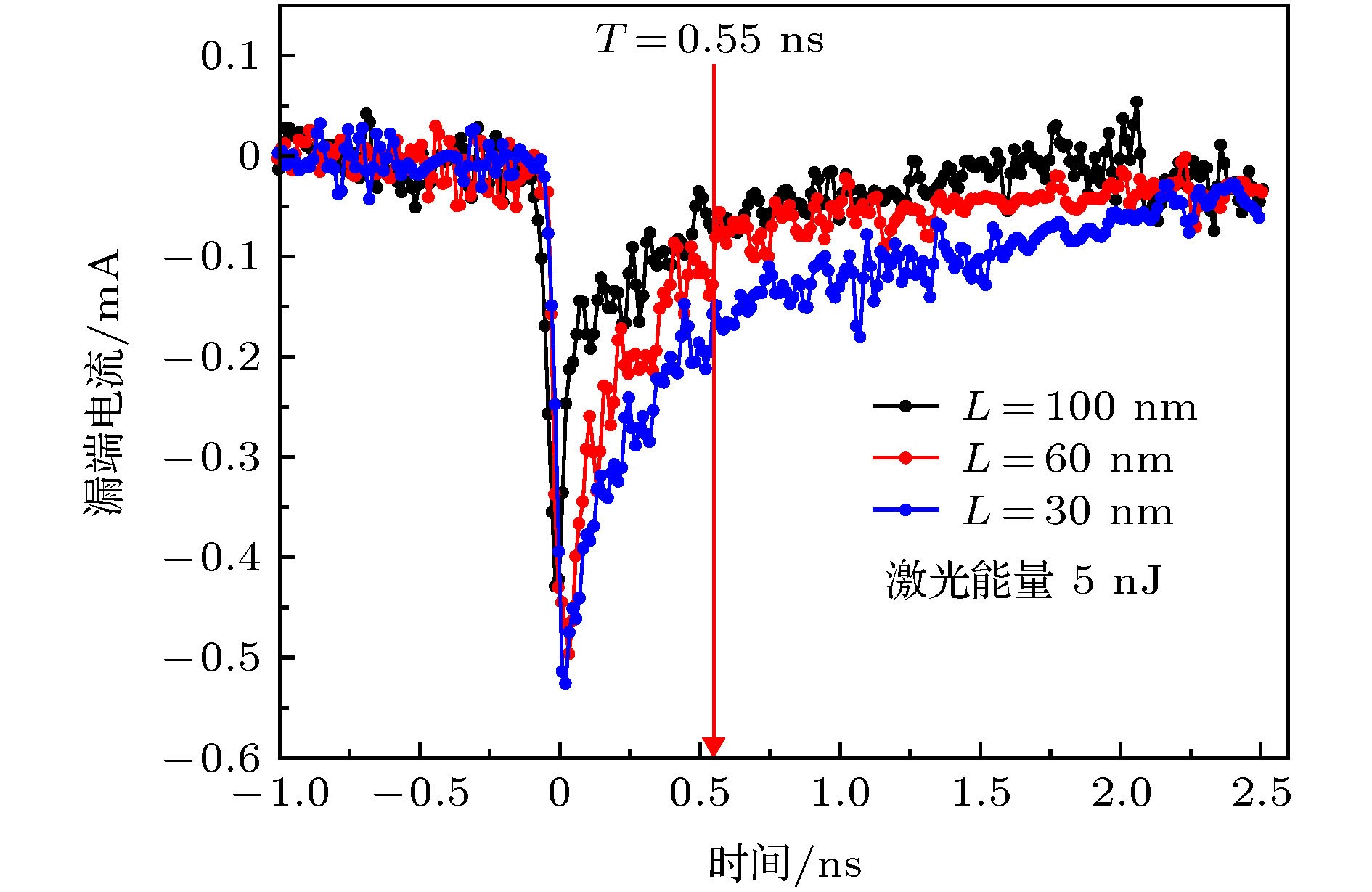
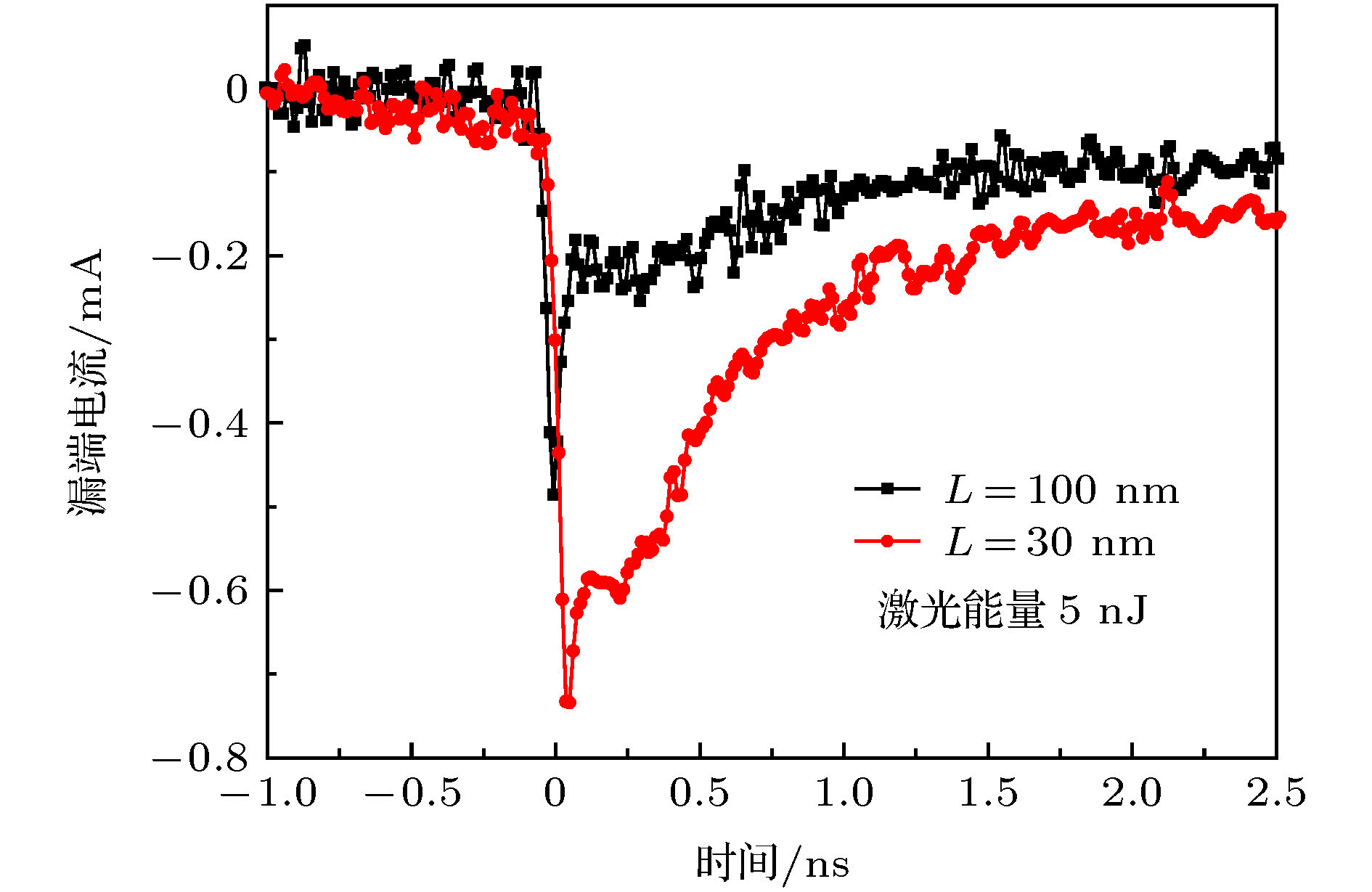
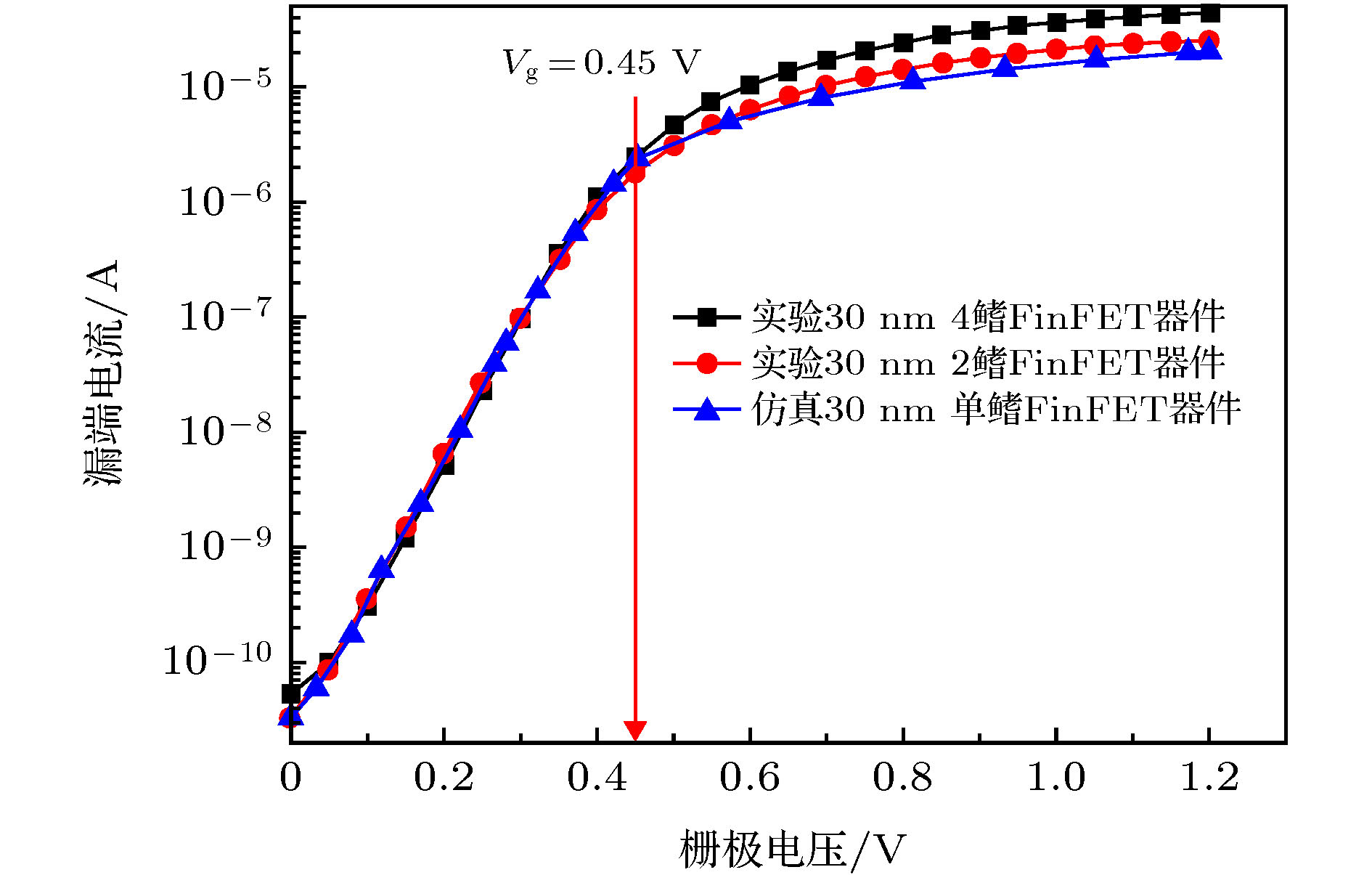
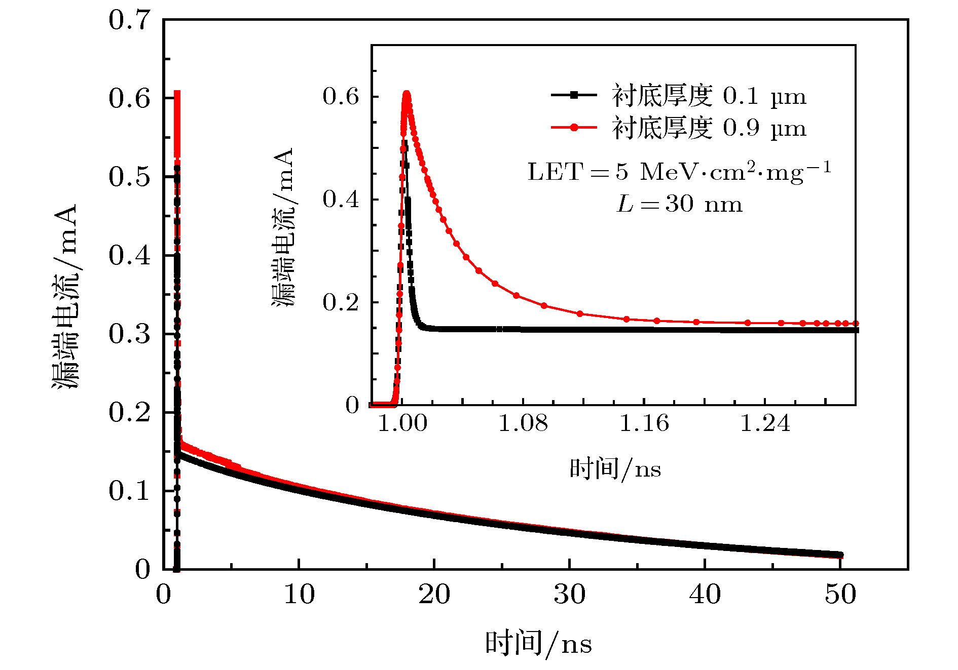
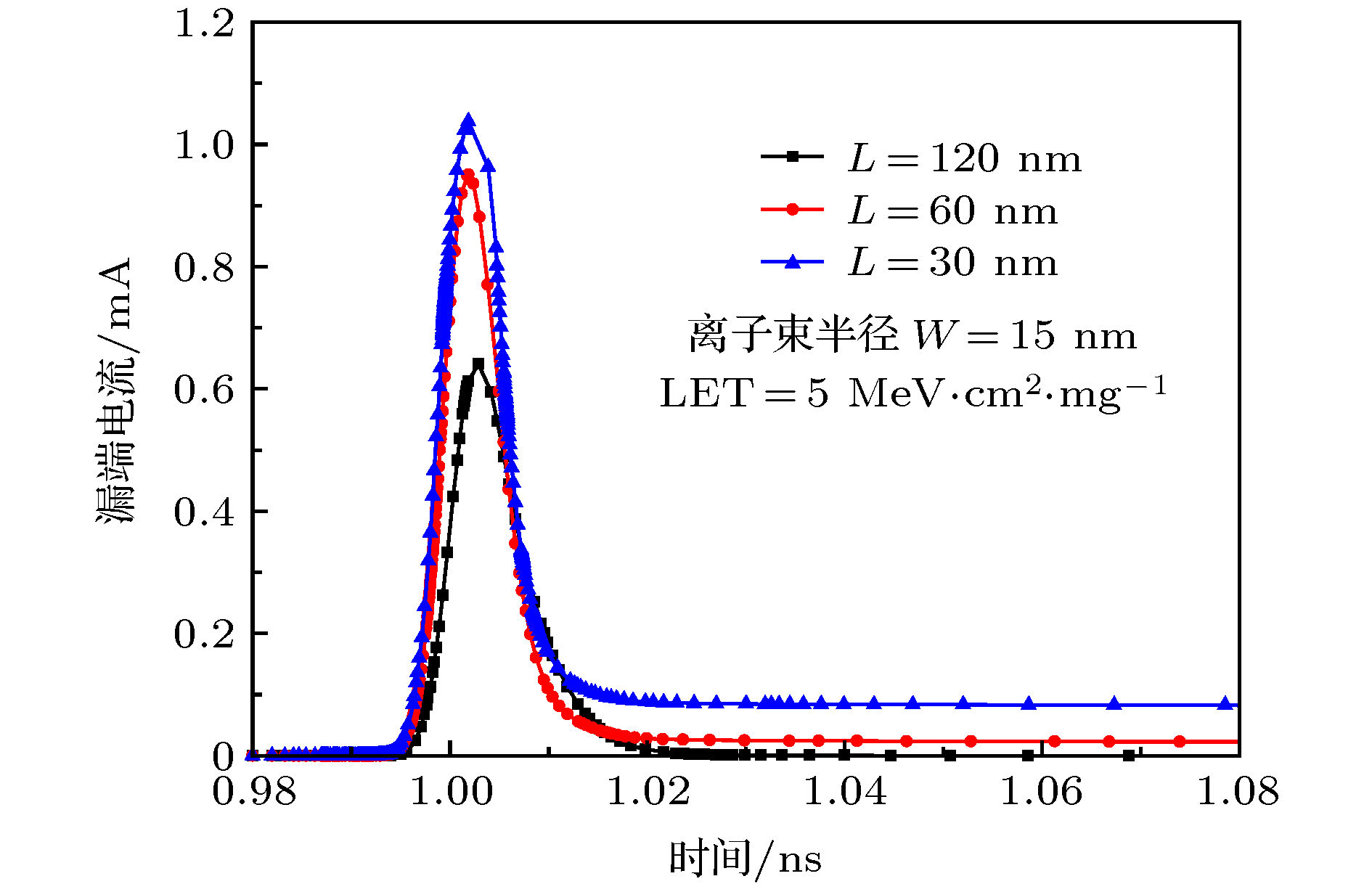
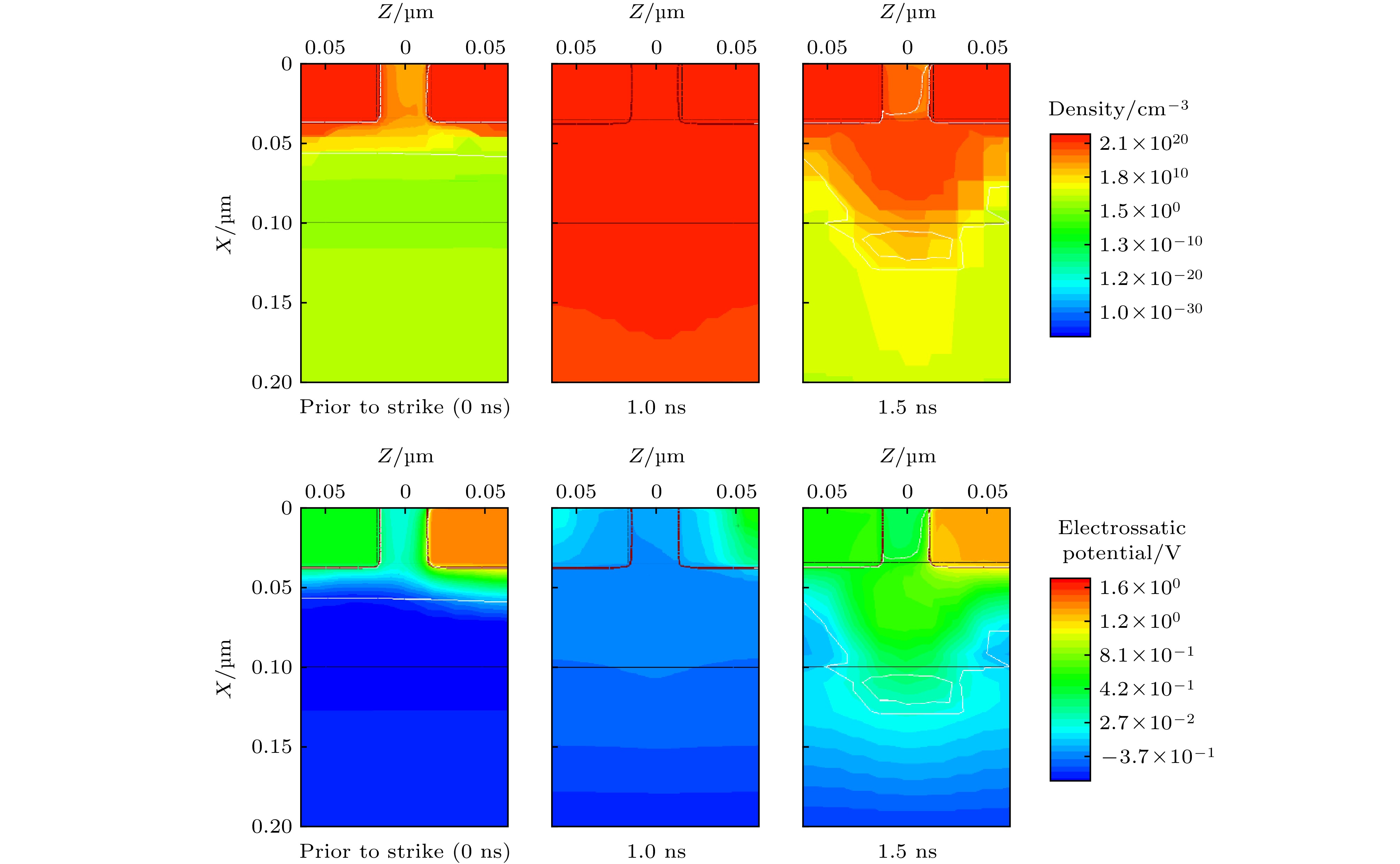
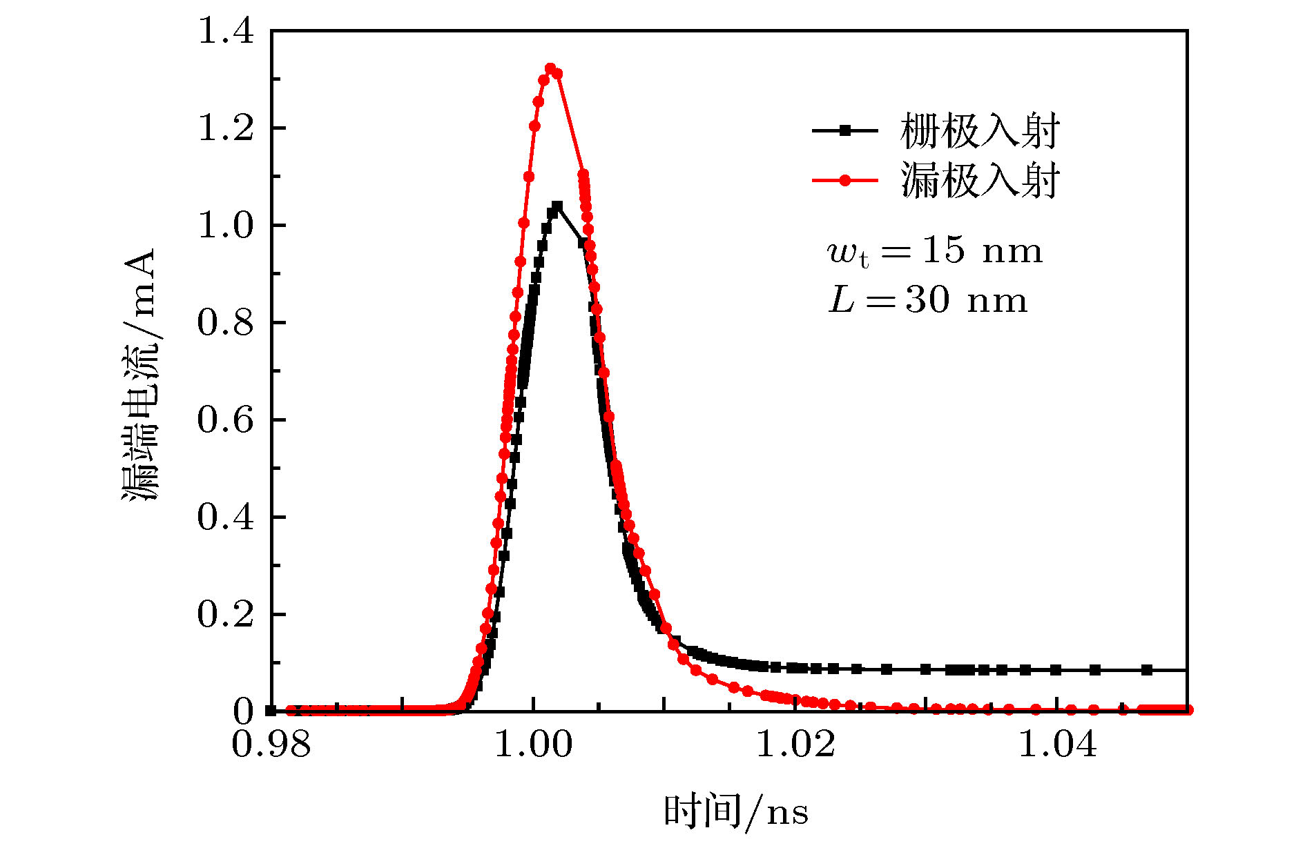
Fin field effect transistor (FinFET) is a most widely used structure when the field effect transistor is scaled down to 30 nm or less. And there are few studies on single-event transient of FinFET devices with gate length below 30 nm. The single-event-transient on FinFET with gate length below 30 nm is worth studying. The single-event-transient responses of bulk FinFETs with 30 nm, 40 nm, 60 nm and 100 nm gate length are examined by using the pulsed laser and technology computer-aided design (TCAD) simulation in this article. First, we use the pulsed laser to ionize the gate of the FinFET device and detect the transient drain current of the FinFET device. The experimental results show that there are obvious platforms for the transient drain current tails of FinFETs with different gate lengths, and the platform current increases as the gate length of FinFET becomes shorter. The charges collected in the platform of FinFET devices with gate lengths of 100, 60, 40, and 30 nm are 34%, 40%, 51%, and 65% of the total charge collected in transient drain current, respectively. Therefore, when the FinFET device with the gate length below 100 nm, the platform current will seriously affect the device performance. Second, we use TCAD to simulate the heavy ion single-event effect of FinFET device and study the generation mechanism of platform region in transient drain current. The TCAD simulation explains this mechanism. Laser or heavy ions ionize high concentration electron-hole pairs in the device. The holes are quickly collected and the high concentration electrons are left under the FinFET channel. High concentration electrons conduct source and drain, generating the source-to-drain current at the tail of the transient drain current. Moreover the source-drain conduction enhances the electrostatic potential below the FinFET channel and suppresses high-concentration electron diffusion, making source-to-drain current decrease slowly and form the platform. The transient drain current tail has a long duration and a large quantity of collected charges, which seriously affects FinFET performance. This is a problem that needs studying in the single-event effect of FinFET device. It is also a problem difficult to solve when the FinFET devices are applied to spacecraft. And the generation mechanism of the transient drain current plateau region of FinFET device can provide theoretical guidance for solving these problems.
-
Keywords:
- single-event transient /
- source-drain conduction /
- platform current
[1] Colinge J P 2008 FinFETs and Other Multi-Gate Transistors (New York: Springer) pp257–258
[2] Herman C H J, Michiel S M, van AHM Arthur R 2011 Analog Circuit Design-Robust Design, Sigma Delta Converters, RFID (New York: Springer) pp69–87
[3] Nsengiyumva P, Ball D R, Kauppila J S, Tam N, McCurdy M, Holman W T, Alles M L, Bhuva B L, Massengill L W 2016 IEEE Trans. Nucl. Sci. 63 266
 Google Scholar
[4] Nsengiyumva P, Massengill L W, Alles M L, Bhuva B L, Ball D R, Kauppila J S, Haeffner T D, Holman W T, Reed R A 2017 IEEE Trans. Nucl. Sci. 64 441
 Google Scholar
[5] Zhang H F, Jiang H, Assis T R, et al. 2017 IEEE Trans. Nucl. Sci. 64 457
 Google Scholar
[6] Nsengiyumva P, Massengill L W, Kauppila J S, Maharrey J A, Harrington R C, Haeffner T D, Ball D R, Alles M L, Bhuva B L, Holman W T, Zhang E X, Rowe J D, Sternberg A L 2018 IEEE Trans. Nucl. Sci. 65 223
 Google Scholar
[7] Narasimham B, Hatami S, Anvar A, Harris D M, Lin A, Wang J K, Chatterjee I, Ni K, Bhuva B L, Schrimpf R D, Reed R A, McCurdy M W 2015 IEEE Trans. Nucl. Sci. 62 2578
 Google Scholar
[8] Harrington R C, Maharrey J A, Kauppila J S, Nsengiyumva P, Ball D R, Haeffner T D, Zhang E X, Bhuva B L, Massengill L W 2018 IEEE Trans. Nucl. Sci. 65 1807
 Google Scholar
[9] Karp J, Hart M J, Maillard P, Hellings G, Linten D 2018 IEEE Trans. Nucl. Sci. 65 217
 Google Scholar
[10] Gong H Q, Ni K, Zhang E X, Sternberg A L, Kozub J A, Ryder K L, Keller R F, Ryder L D, Weiss S M, Weller R A, Alles M L, Reed R A, Fleetwood D M, Schrimpf R D, Vardi A, Jesús A 2018 IEEE Trans. Nucl. Sci. 65 296
 Google Scholar
[11] Gong H Q, Ni K, Zhang E X, Sternberg A L, Kozub J A, Alles M L, Reed R A, Fleetwood D M, Schrimpf R D, Waldron N, Kunert B, Linten D 2019 IEEE Trans. Nucl. Sci. 66 376
 Google Scholar
[12] Ni K, Sternberg A L, Zhang E X, Kozub J A, Rong J, Schrimpf R D, Reed R A, Fleetwood D M, Alles M L, McMorrow D, Lin J Q, Vardi A, Jesús A 2017 IEEE Trans. Nucl. Sci. 64 2069
 Google Scholar
[13] El-Mamouni F, Zhang E X, Pate N D, Hooten N, Schrimpf R D, Reed R A, Galloway K F, McMorrow D, Warner J, Simoen E, Claeys C, Griffoni A, Linten D, Vizkelethy G 2011 IEEE Trans. Nucl. Sci. 58 2563
 Google Scholar
[14] El-Mamouni F, Zhang E X, Ball D R, Sierawski B, King M P, Schrimpf R D, Reed R A, Alles M L, Fleetwood D M, Linten D, Simoen E, Vizkelethy G 2012 IEEE Trans. Nucl. Sci. 59 2674
 Google Scholar
[15] 于俊庭 2017 博士学位论文 (长沙: 国防科技大学)
Yu J T 2017 Ph. D. Dissertation (Changsha: National University of Defense Technology) (in Chinese)
[16] Yu J T, Chen S M, Chen J J, Huang P C, Song R Q 2016 Chin. Phys. B 25 049401
 Google Scholar
[17] Yu J T, Chen S M, Chen J J, Huang P C 2015 Chin. Phys. B 24 119401
 Google Scholar
[18] Wu Z Y, Zhu B N, Yi T Y, Li C, Liu Y, Yang Y T 2018 J. Comput. Electron. 17 1608
 Google Scholar
[19] Li G S, An X, Ren Z X, Wang J N, Huang R 2018 IEEE International Conference on Solid-State and Integrated Circuit Technology (ICSICT) Qingdao, China, Oct. 31–Nov. 3, 2018 p1
[20] 田恺, 曹洲, 薛玉雄, 杨世宇 2010 原子能科学技术 44 489
Tian K, Cao Z, Xue Y X, Yang S Y 2010 At. Energ. Sci. Technol. 44 489
[21] 黄建国, 韩建伟 2004 中国科学G辑: 物理学 力学 天文学 34 601
Haung J G, Han J W 2004 Science in China Series G: Physics, Mechanics & Astronomy 34 601
[22] Adams J H 1983 IEEE Trans. Nucl. Sci. 30 4475
 Google Scholar
[23] 卓青青, 刘红侠, 郝跃 2012 61 218501
 Google Scholar
Zhuo Q Q, Liu H X, Hao Y 2012 Acta Phys. Sin. 61 218501
 Google Scholar
-
-
[1] Colinge J P 2008 FinFETs and Other Multi-Gate Transistors (New York: Springer) pp257–258
[2] Herman C H J, Michiel S M, van AHM Arthur R 2011 Analog Circuit Design-Robust Design, Sigma Delta Converters, RFID (New York: Springer) pp69–87
[3] Nsengiyumva P, Ball D R, Kauppila J S, Tam N, McCurdy M, Holman W T, Alles M L, Bhuva B L, Massengill L W 2016 IEEE Trans. Nucl. Sci. 63 266
 Google Scholar
[4] Nsengiyumva P, Massengill L W, Alles M L, Bhuva B L, Ball D R, Kauppila J S, Haeffner T D, Holman W T, Reed R A 2017 IEEE Trans. Nucl. Sci. 64 441
 Google Scholar
[5] Zhang H F, Jiang H, Assis T R, et al. 2017 IEEE Trans. Nucl. Sci. 64 457
 Google Scholar
[6] Nsengiyumva P, Massengill L W, Kauppila J S, Maharrey J A, Harrington R C, Haeffner T D, Ball D R, Alles M L, Bhuva B L, Holman W T, Zhang E X, Rowe J D, Sternberg A L 2018 IEEE Trans. Nucl. Sci. 65 223
 Google Scholar
[7] Narasimham B, Hatami S, Anvar A, Harris D M, Lin A, Wang J K, Chatterjee I, Ni K, Bhuva B L, Schrimpf R D, Reed R A, McCurdy M W 2015 IEEE Trans. Nucl. Sci. 62 2578
 Google Scholar
[8] Harrington R C, Maharrey J A, Kauppila J S, Nsengiyumva P, Ball D R, Haeffner T D, Zhang E X, Bhuva B L, Massengill L W 2018 IEEE Trans. Nucl. Sci. 65 1807
 Google Scholar
[9] Karp J, Hart M J, Maillard P, Hellings G, Linten D 2018 IEEE Trans. Nucl. Sci. 65 217
 Google Scholar
[10] Gong H Q, Ni K, Zhang E X, Sternberg A L, Kozub J A, Ryder K L, Keller R F, Ryder L D, Weiss S M, Weller R A, Alles M L, Reed R A, Fleetwood D M, Schrimpf R D, Vardi A, Jesús A 2018 IEEE Trans. Nucl. Sci. 65 296
 Google Scholar
[11] Gong H Q, Ni K, Zhang E X, Sternberg A L, Kozub J A, Alles M L, Reed R A, Fleetwood D M, Schrimpf R D, Waldron N, Kunert B, Linten D 2019 IEEE Trans. Nucl. Sci. 66 376
 Google Scholar
[12] Ni K, Sternberg A L, Zhang E X, Kozub J A, Rong J, Schrimpf R D, Reed R A, Fleetwood D M, Alles M L, McMorrow D, Lin J Q, Vardi A, Jesús A 2017 IEEE Trans. Nucl. Sci. 64 2069
 Google Scholar
[13] El-Mamouni F, Zhang E X, Pate N D, Hooten N, Schrimpf R D, Reed R A, Galloway K F, McMorrow D, Warner J, Simoen E, Claeys C, Griffoni A, Linten D, Vizkelethy G 2011 IEEE Trans. Nucl. Sci. 58 2563
 Google Scholar
[14] El-Mamouni F, Zhang E X, Ball D R, Sierawski B, King M P, Schrimpf R D, Reed R A, Alles M L, Fleetwood D M, Linten D, Simoen E, Vizkelethy G 2012 IEEE Trans. Nucl. Sci. 59 2674
 Google Scholar
[15] 于俊庭 2017 博士学位论文 (长沙: 国防科技大学)
Yu J T 2017 Ph. D. Dissertation (Changsha: National University of Defense Technology) (in Chinese)
[16] Yu J T, Chen S M, Chen J J, Huang P C, Song R Q 2016 Chin. Phys. B 25 049401
 Google Scholar
[17] Yu J T, Chen S M, Chen J J, Huang P C 2015 Chin. Phys. B 24 119401
 Google Scholar
[18] Wu Z Y, Zhu B N, Yi T Y, Li C, Liu Y, Yang Y T 2018 J. Comput. Electron. 17 1608
 Google Scholar
[19] Li G S, An X, Ren Z X, Wang J N, Huang R 2018 IEEE International Conference on Solid-State and Integrated Circuit Technology (ICSICT) Qingdao, China, Oct. 31–Nov. 3, 2018 p1
[20] 田恺, 曹洲, 薛玉雄, 杨世宇 2010 原子能科学技术 44 489
Tian K, Cao Z, Xue Y X, Yang S Y 2010 At. Energ. Sci. Technol. 44 489
[21] 黄建国, 韩建伟 2004 中国科学G辑: 物理学 力学 天文学 34 601
Haung J G, Han J W 2004 Science in China Series G: Physics, Mechanics & Astronomy 34 601
[22] Adams J H 1983 IEEE Trans. Nucl. Sci. 30 4475
 Google Scholar
[23] 卓青青, 刘红侠, 郝跃 2012 61 218501
 Google Scholar
Zhuo Q Q, Liu H X, Hao Y 2012 Acta Phys. Sin. 61 218501
 Google Scholar
Catalog
Metrics
- Abstract views: 9862
- PDF Downloads: 92
- Cited By: 0


 DownLoad:

