-
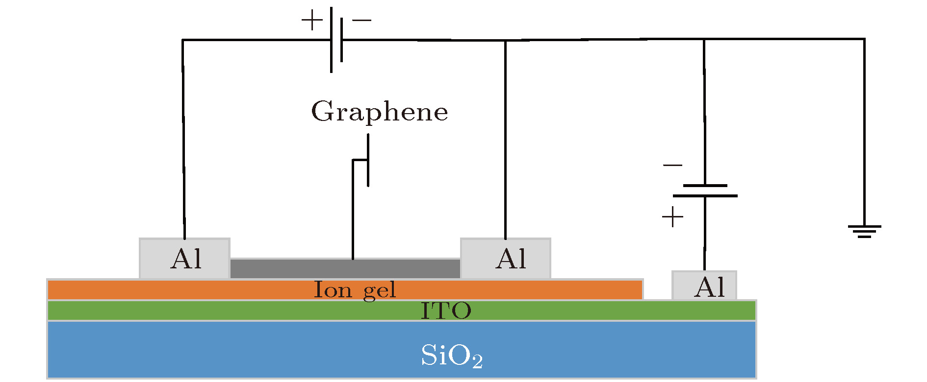
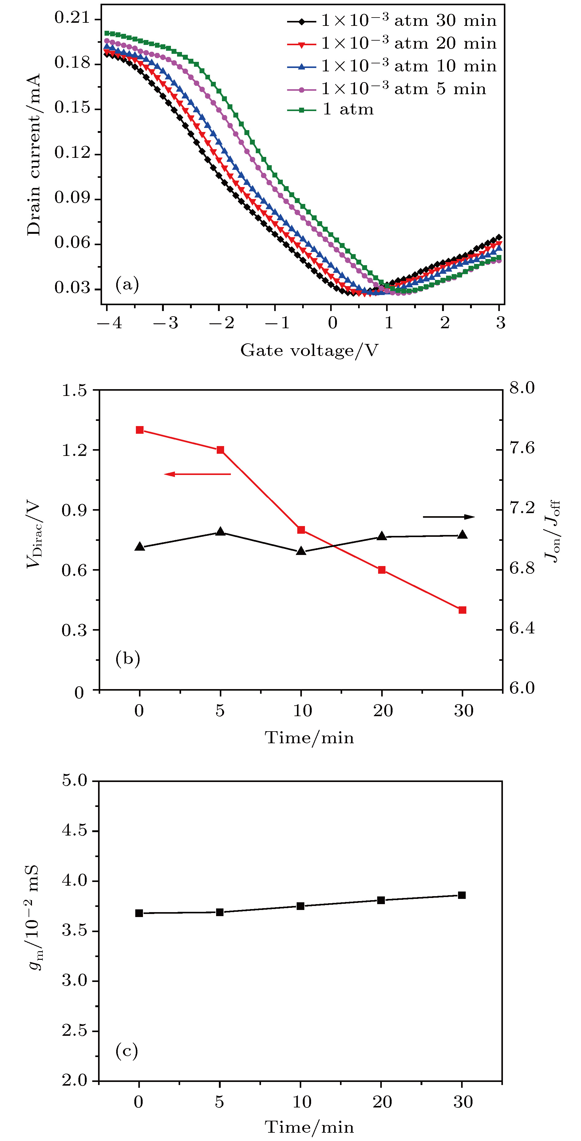
Graphene is a kind of two-dimensional material with high light transmittance, high mechanical properties and high carrier mobility. The energy band of graphene can be turned by doping and electric field. Researches on the application of graphene to electronic devices focused on field effect transistors. For improving the performance, one generally improves the fabrication process and device structure, but many researchers chose to change the material or structure of dielectric layer. Ion-gel is a kind of mixture of organic polymer mesh structure with good thermal stability and high dielectric value, prepared by macromolecule organic polymer and ionic salt electrolyte material. With the effect of electric field, cations and anions in ion-gel diffuse to form a double charge layer distribution with a charge layer on the surface of material. This capacitance characteristic is similar to that of traditional capacitor. In this paper, ion-gel (PVDF-[EMIM]TF2N) film is used as a dielectric layer material to prepare the bottom-gate graphene-based field effect transistor (GFET), which is compared with the GFET with SiO2 bottom-gate, according to electrical characteristic curves. The effect of the ion-gel film on the transconductance, switching ratio and Dirac voltage of the GFET are analyzed. The effect of the vacuum environment and temperature on the GFET performance with ion-gel film gate are also investigated. The results show that in the room-temperature environment, the switching ratio and transconductance of the ion-gel film gate GFET device increase to 6.95 and 3.68 × 10⁻² mS, respectively, compared with those of the SiO2 gate GFET, while the Dirac voltage decreases to 1.3 V. The increase in transconductance and switching ratio of ion-gel film gate GFETs are mainly due to the high capacitance of ion-gel film compared with those of conventional SiO2 gate dielectrics. There will be more carriers inside the graphene while in the carrier accumulation region of GFET transfer characteristic curve, which makes graphene more conductive. The Dirac voltage of ion-gel film gate GFET can be reduced to 0.4 V in the vacuum environment; as the temperature increases, the transconductance of GFET can increase up to 6.11×10⁻² mS. The results indicate that the ion-gel film-based graphene field effect transistor shows good electrical properties in serving as high dielectric constant organic dielectric materials.
-
Keywords:
- graphene /
- ion-gel film /
- field effect transistor /
- electrical properties
[1] Bolotin K I, Sikes K J, Jiang Z, Klima M, Fudenberg G, Hone J, Kim P, Stormer H L 2008 Solid State Commun. 146 351
 Google Scholar
[2] Novoselov K S, Geim A K, Morozov S V, Jiang D, Zhang Y, Dubonos S V, Grigorieva I V, Firsov A A 2004 Science 306 666
 Google Scholar
[3] Zhang Y, Tang T, Girit C, Hao Z, Martin M C, Zettl A, Crommie M F, Shen Y R, Wang F 2009 Nature 459 820
 Google Scholar
[4] Park J S, Choi H J 2015 Phys. Rev. B 92 045402
 Google Scholar
[5] 刘贵立, 杨忠华 2018 67 076301
 Google Scholar
Liu G L, Yang Z H 2018 Acta Phys. Sin. 67 076301
 Google Scholar
[6] Lemme M C, Echtermeyer T J, Baus M, Kurz H 2007 IEEE Electr. Dev. Lett. 28 282
 Google Scholar
[7] Frank S 2010 Nat. Nanotechnol. 5 487
 Google Scholar
[8] Li X L, Wang X R, Zhang L, Lee S, Dai H J 2008 Science 319 1229
 Google Scholar
[9] Echtermeyer T J, Lemme M C, Bolten J, Baus M, Ramsteiner M, Kurz H 2007 Eur. Phys. J. Spec. Top. 148 19
 Google Scholar
[10] Shih C J, Pfattner R, Chiu Y C, Liu N, Lei T, Kong D, Kim Y, Chou H H, Bae W G, Bao Z 2015 Nano Lett. 15 7587
 Google Scholar
[11] Fallahazad B, Lee K, Lian G, Kim S, Corbet C M, Ferrer D A, Colombo L, Tutuc E 2012 Appl. Phys. Lett. 100 093112
 Google Scholar
[12] Wang B, Liddell K L, Wang J, Koger B, Keating C D, Zhu J 2014 Nano Res. 7 1263
 Google Scholar
[13] 吴春艳, 杜晓薇, 周麟, 蔡奇, 金妍, 唐琳, 张菡阁, 胡国辉, 金庆辉 2016 65 080701
 Google Scholar
Wu C Y, Du X W, Zhou L, Cai Q, Jin Y, Tang L, Zhang H G, Hu G H, Jin Q H 2016 Acta Phys. Sin. 65 080701
 Google Scholar
[14] Kim B J, Jang H, Lee S K, Hong B H, Ahn J H, Cho J H 2010 Nano Lett. 10 3464
 Google Scholar
[15] Lee S K, Kim B J, Jang H, Yoon S C, Lee C, Hong B H, Rogers J A, Cho J H, Ahn J H 2011 Nano Lett. 11 4642
 Google Scholar
[16] Bard A J, Faulkner L R 2002 Electrochemical Methods. Fundamentals and Applications (2nd Ed.) (Weinheim: WILEY-VCH Verlag GmbH)
[17] Cho J H, Lee J, Xia Y, Kim B S, He Y, Renn M J, Lodge T P, Frisbie C D 2008 Nat. Mater. 7 900
 Google Scholar
[18] Li X, Zhu Y, Cai W, Borysiak M, Han B, Chen D, Piner R D, Colombo L, Ruoff R S 2009 Nano Lett. 9 4359
 Google Scholar
[19] Kim K S, Zhao Y, Jang H, Lee S Y, Kim J M, Kim K S, Ahn J H, Kim P, Choi J Y, Hong B H 2009 Nature 457 706
 Google Scholar
[20] Beams R, Novotny L 2015 J. Phys.: Condens. Matter 27 83002
 Google Scholar
[21] Ryu S, Liu L, Berciaud S, Yu Y J, Liu H, Kim P, Flynn G W, Brus L E 2010 Nano Lett. 10 4944
 Google Scholar
[22] Yang Y, Brenner K, Murali R 2012 Carbon 50 1727
 Google Scholar
[23] Jürgen R 2006 Science 313 1057
 Google Scholar
[24] Robitaille C D, Fauteux D 1986 J. Electrochem. Soc. 133 315
 Google Scholar
[25] Geim A K, Novoselov K S 2010 The Rise of Graphene (Nanoscience and Technology: A Collection of Reviews from Nature Journals (Singapore: World Scientific) pp 11–19
[26] Gierz I, Riedl C, Starke U, Ast C R, Kern K 2008 Nano Lett. 8 4603
 Google Scholar
[27] Liu H, Liu Y, Zhu D 2011 J. Mater. Chem. 21 3335
 Google Scholar
-
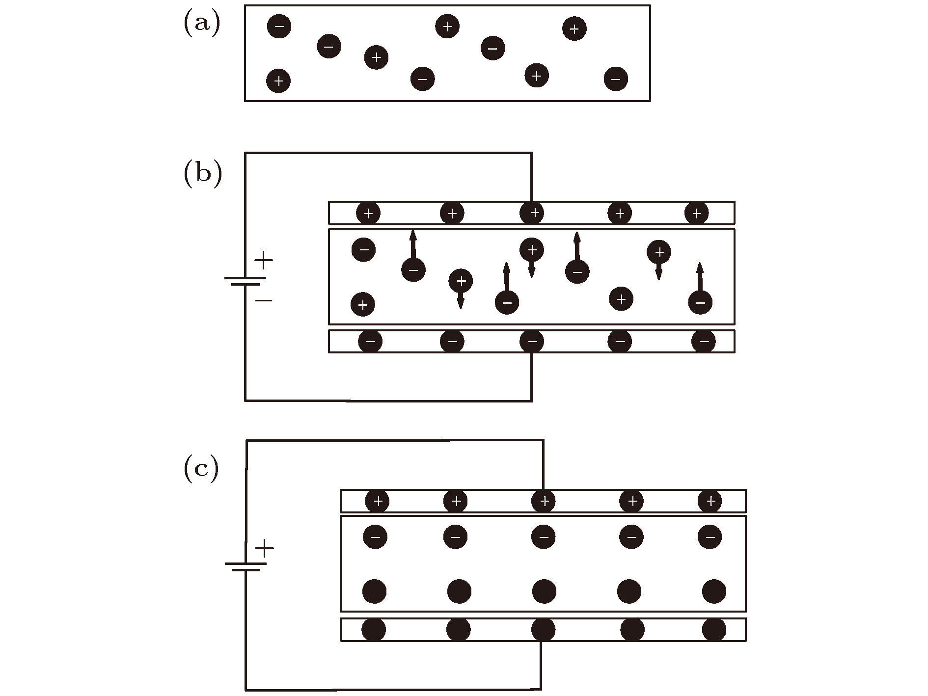
图 1 GCS模型双电荷层分布示意图 (a) 阴阳离子分散在电介质中; (b) 在外电场作用下, 电介质内部阴阳离子开始向两级移动; (c) 达到平衡后, 电介质内阴阳离子排布情况
Figure 1. Schematic diagram of GCS model with dual-charge layer distribution: (a) The anions are dispersed in dielectric; (b) under the action of electric field, the anions and cations begin to move in the opposite direction; (c) the distribution of anions and cations in dielectric in equilibrium
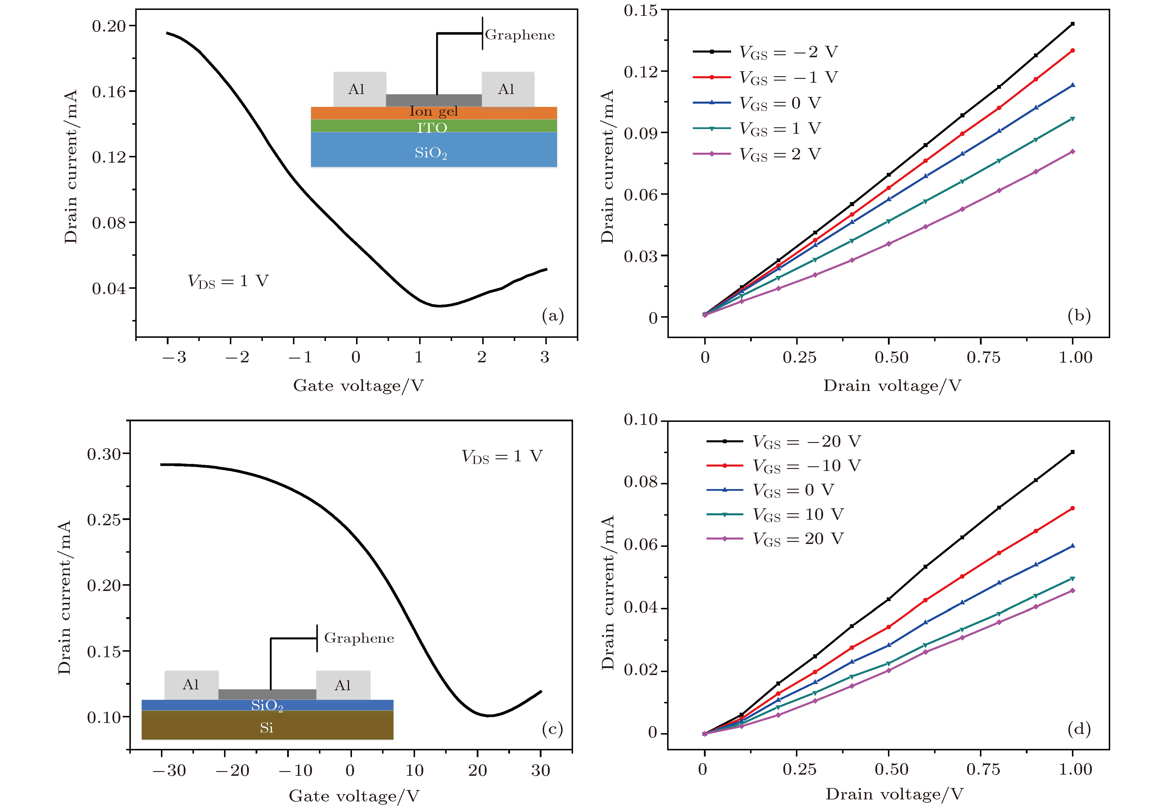
图 8 室温环境下GFET电学特性曲线 (a)离子凝胶栅介GFET的转移特性曲线; (b)离子凝胶栅介GFET的输出特性曲线; (c) SiO2栅介GFET的转移特性曲线; (d) SiO2栅介GFET的输出特性曲线
Figure 8. Electrical characteristic curves of GFET at room temperature: (a) The transfer characteristic curve of GFET with ion-gel film gate; (b) the output characteristic curve of GFET with ion-gel film gate; (c) the transfer characteristic curve of GFET with SiO2 gate; (d) the output characteristic curve of GFET with SiO2 gate
-
[1] Bolotin K I, Sikes K J, Jiang Z, Klima M, Fudenberg G, Hone J, Kim P, Stormer H L 2008 Solid State Commun. 146 351
 Google Scholar
[2] Novoselov K S, Geim A K, Morozov S V, Jiang D, Zhang Y, Dubonos S V, Grigorieva I V, Firsov A A 2004 Science 306 666
 Google Scholar
[3] Zhang Y, Tang T, Girit C, Hao Z, Martin M C, Zettl A, Crommie M F, Shen Y R, Wang F 2009 Nature 459 820
 Google Scholar
[4] Park J S, Choi H J 2015 Phys. Rev. B 92 045402
 Google Scholar
[5] 刘贵立, 杨忠华 2018 67 076301
 Google Scholar
Liu G L, Yang Z H 2018 Acta Phys. Sin. 67 076301
 Google Scholar
[6] Lemme M C, Echtermeyer T J, Baus M, Kurz H 2007 IEEE Electr. Dev. Lett. 28 282
 Google Scholar
[7] Frank S 2010 Nat. Nanotechnol. 5 487
 Google Scholar
[8] Li X L, Wang X R, Zhang L, Lee S, Dai H J 2008 Science 319 1229
 Google Scholar
[9] Echtermeyer T J, Lemme M C, Bolten J, Baus M, Ramsteiner M, Kurz H 2007 Eur. Phys. J. Spec. Top. 148 19
 Google Scholar
[10] Shih C J, Pfattner R, Chiu Y C, Liu N, Lei T, Kong D, Kim Y, Chou H H, Bae W G, Bao Z 2015 Nano Lett. 15 7587
 Google Scholar
[11] Fallahazad B, Lee K, Lian G, Kim S, Corbet C M, Ferrer D A, Colombo L, Tutuc E 2012 Appl. Phys. Lett. 100 093112
 Google Scholar
[12] Wang B, Liddell K L, Wang J, Koger B, Keating C D, Zhu J 2014 Nano Res. 7 1263
 Google Scholar
[13] 吴春艳, 杜晓薇, 周麟, 蔡奇, 金妍, 唐琳, 张菡阁, 胡国辉, 金庆辉 2016 65 080701
 Google Scholar
Wu C Y, Du X W, Zhou L, Cai Q, Jin Y, Tang L, Zhang H G, Hu G H, Jin Q H 2016 Acta Phys. Sin. 65 080701
 Google Scholar
[14] Kim B J, Jang H, Lee S K, Hong B H, Ahn J H, Cho J H 2010 Nano Lett. 10 3464
 Google Scholar
[15] Lee S K, Kim B J, Jang H, Yoon S C, Lee C, Hong B H, Rogers J A, Cho J H, Ahn J H 2011 Nano Lett. 11 4642
 Google Scholar
[16] Bard A J, Faulkner L R 2002 Electrochemical Methods. Fundamentals and Applications (2nd Ed.) (Weinheim: WILEY-VCH Verlag GmbH)
[17] Cho J H, Lee J, Xia Y, Kim B S, He Y, Renn M J, Lodge T P, Frisbie C D 2008 Nat. Mater. 7 900
 Google Scholar
[18] Li X, Zhu Y, Cai W, Borysiak M, Han B, Chen D, Piner R D, Colombo L, Ruoff R S 2009 Nano Lett. 9 4359
 Google Scholar
[19] Kim K S, Zhao Y, Jang H, Lee S Y, Kim J M, Kim K S, Ahn J H, Kim P, Choi J Y, Hong B H 2009 Nature 457 706
 Google Scholar
[20] Beams R, Novotny L 2015 J. Phys.: Condens. Matter 27 83002
 Google Scholar
[21] Ryu S, Liu L, Berciaud S, Yu Y J, Liu H, Kim P, Flynn G W, Brus L E 2010 Nano Lett. 10 4944
 Google Scholar
[22] Yang Y, Brenner K, Murali R 2012 Carbon 50 1727
 Google Scholar
[23] Jürgen R 2006 Science 313 1057
 Google Scholar
[24] Robitaille C D, Fauteux D 1986 J. Electrochem. Soc. 133 315
 Google Scholar
[25] Geim A K, Novoselov K S 2010 The Rise of Graphene (Nanoscience and Technology: A Collection of Reviews from Nature Journals (Singapore: World Scientific) pp 11–19
[26] Gierz I, Riedl C, Starke U, Ast C R, Kern K 2008 Nano Lett. 8 4603
 Google Scholar
[27] Liu H, Liu Y, Zhu D 2011 J. Mater. Chem. 21 3335
 Google Scholar
Catalog
Metrics
- Abstract views: 13498
- PDF Downloads: 203
- Cited By: 0


 DownLoad:


