-
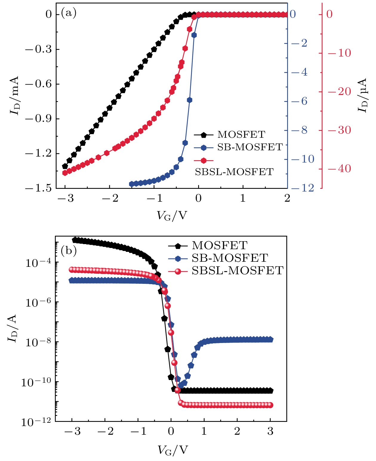
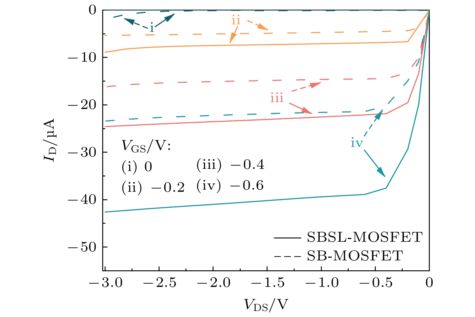
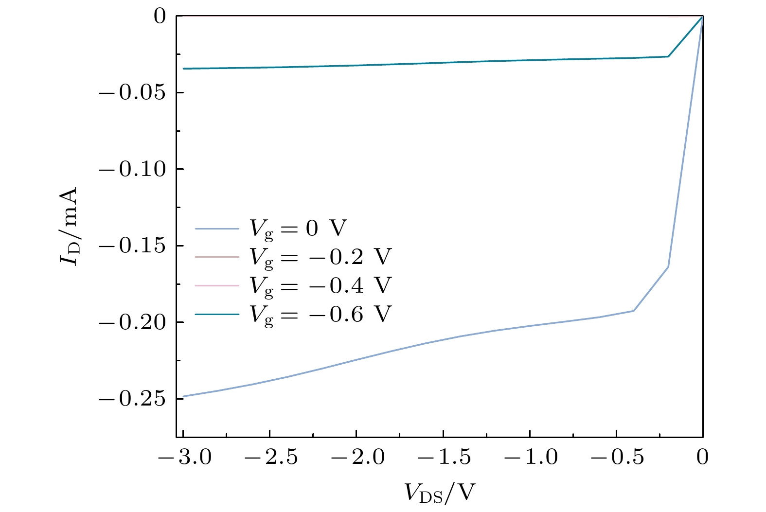
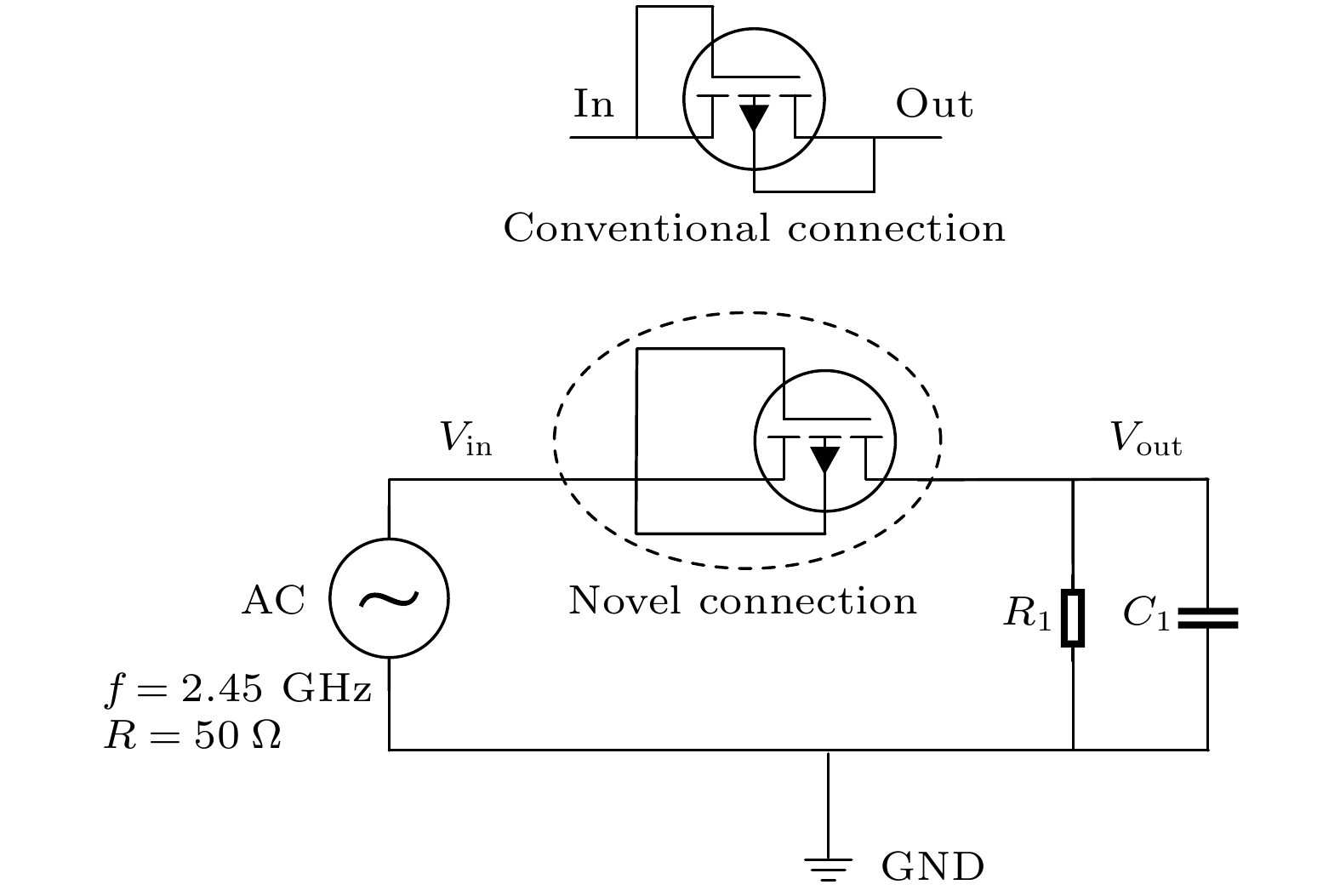
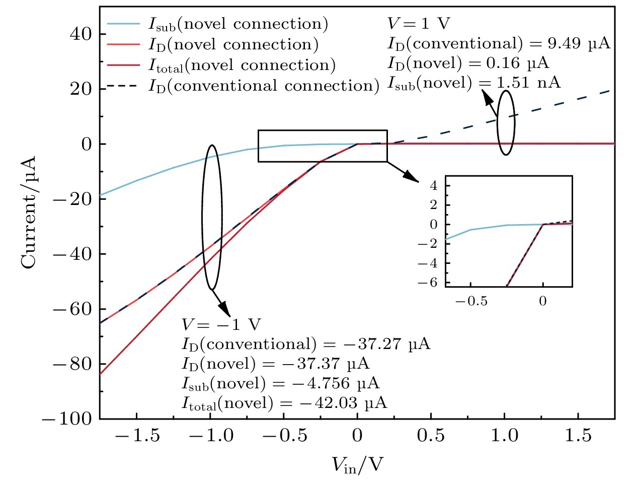
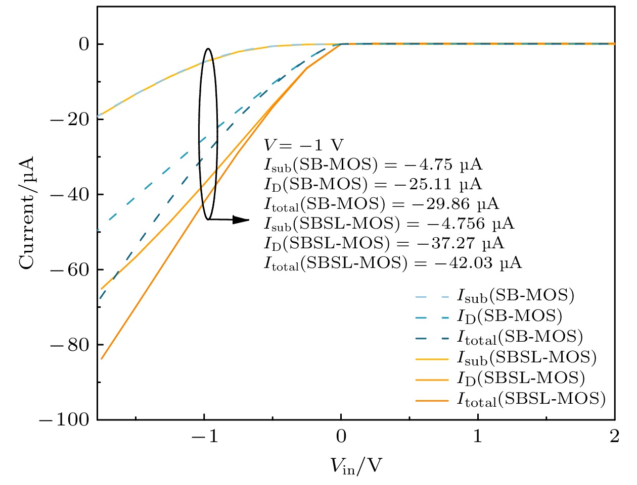
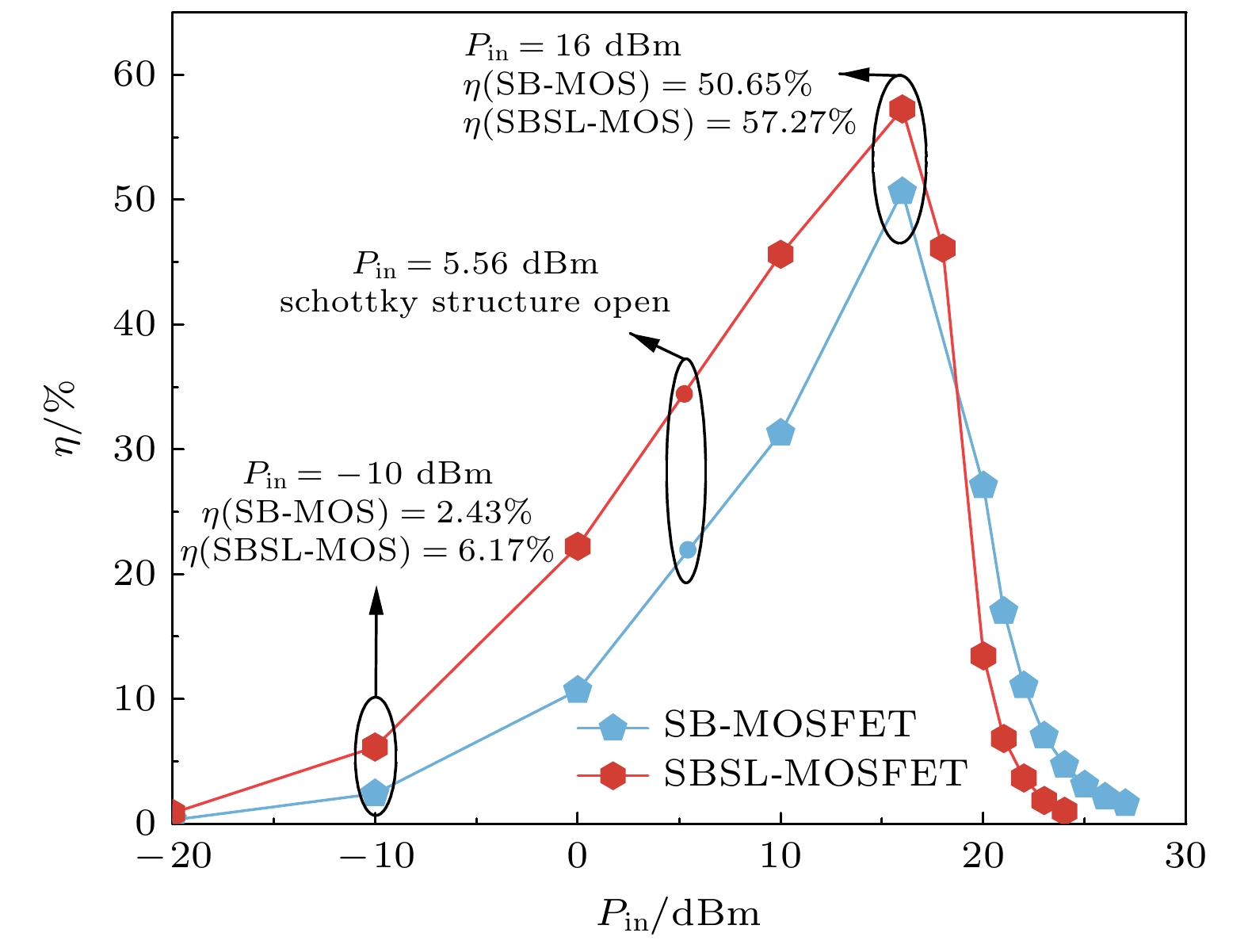
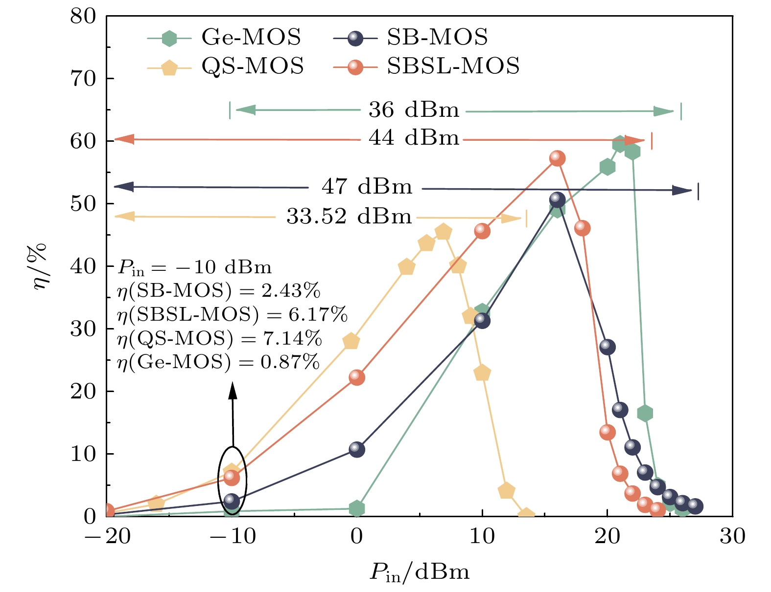
Rectifier component is a core part of a microwave wireless energy transmission system, and the development of new rectifier components is an important research direction in this field. Schottky diodes and field-effect transistors are currently the mainstream rectifier devices, but they have a limited rectification range and cannot achieve a wide-range rectification of both weak energy and medium energy density at the same time. In view of this, in this work proposed and designed is a Ge based p-type single-ended Schottky barrier field effect transistor (Schottky contact at the source and standard p+ doping at the drain) for 2.45 GHz microwave wireless energy transmission. Based on this, the Schottky structure of the device is fully utilised and a new diode connection is used in order to realize a dual channel wide range rectification of the trench and source lined Schottky structure opened at different bias voltages. Simulations are carried out by using the Silvaco TCAD software. For a half-wave rectifier circuit with a load of 0.3 pF and 70 kΩ, a wide range from –20 to 24 dBm rectification is achieved, which is 8 dBm wider than the range of Ge field-effect transistors under the same conditions, and the overall rectification efficiency is higher in the range, with a peak rectification efficiency of 57.27% at 16 dBm. The rectification efficiency at –10 dBm weak energy density reaches 6.17%, which is more than 7 times that of Ge FETs under the same conditions.
-
Keywords:
- wireless energy transmission /
- Schottky barrier field effect transistor /
- Schottky contact /
- rectifying efficiency
[1] Ullah M A, Keshavarz R, Abolhasan M, Lipman J, Esselle K P, Shariati N 2022 IEEE Access 10 17231
 Google Scholar
[2] Haerinia M, Shadid R 2020 Signals 1 209
 Google Scholar
[3] Divakaran S K, Krishna D D 2019 INT. J. RF. Microw. C. E 29 e21633
 Google Scholar
[4] Zhang Z, Pang H, Georgiadis A, Cecati C 2019 IEEE Trans. Ind. Electron. 66 1044
 Google Scholar
[5] Eteng A A, Goh H H, Rahim S K A, Alomainy A 2021 IEEE Access 9 27518
 Google Scholar
[6] Zhu G L, Du J X, Yang X X, Zhou Y G, Gao S 2019 IEEE Access 7 141978
 Google Scholar
[7] Xiao H, Zhang H, Song W, Wang J, Chen W, Lu M 2021 IEEE Trans. Ind. Electron. 69 2896
 Google Scholar
[8] 宋建军, 张龙强, 陈雷, 周亮, 孙雷, 兰军峰, 习楚浩, 李家豪 2021 70 108401
 Google Scholar
Song J J, Zhang L Q, Chen L, Zhou L, Sun L, Lan J F, Xi C H, Li J H 2021 Acta Phys. Sin. 70 108401
 Google Scholar
[9] 李妤晨, 陈航宇, 宋建军 2020 69 108401
 Google Scholar
Li Y C, Chen H Y, Song J J 2020 Acta Phys. Sin. 69 108401
 Google Scholar
[10] Chong G, Ramiah H, Yin J, Rajendran J, Mak P I, Martins R P 2019 IEEE Trans. Circuits Syst. II, Exp. Briefs 68 1743
 Google Scholar
[11] Choi W, Lee J, Shin M 2014 IEEE Trans. Electron Devices 61 37
 Google Scholar
[12] Kim S, Lee K, Lee J H, Park B G, Kwon D 2021 IEEE Trans. Electron Devices 68 4754
 Google Scholar
[13] Yao Y, Sun Y, Li X, Shi Y, Liu Z 2020 IEEE Trans. Electron Devices 67 751
 Google Scholar
[14] Chen C W, Tzeng J Y, Chuang C T, Chien H P, Chien C H, Luo G L 2014 IEEE Trans. Electron Devices 61 2656
 Google Scholar
[15] 张茂添 2014 硕士学位论文 (厦门: 厦门大学)
Zhang M T 2014 M. S. Thesis (Xiamen: Xiamen University) (in Chinese)
[16] 施敏, 伍国珏(耿莉, 张瑞智译) 2007 半导体器件物理 (北京: 西安交通大学出版社) 第 130—142页
Sze S M, Kwok K N (translated by Geng L, Zhang R Z) 2007 Physics of Semiconductor Devices (Xi’an: Xi’an jiaotong University Press) pp130–142 (in Chinese)
[17] 汤晓燕 2007博士学位论文 (西安: 西安电子科技大学)
Tang X Y 2007 Ph. D. Dissertation (Xi’an: Xidian University) (in Chinese)
[18] Shokrani M R, Hamidon M N, Khoddam M, Najafi V 2012 IEEE International Conference on Electronics Design Kuala Lumpur, Malaysia, November 5–6, 2012 p234
[19] Shokrani M R, Khoddam M, Hamidon M N B, Kamsani N A, Rokhani F Z, Shafie S B 2014 Sci. World J. 2014 1
 Google Scholar
[20] Zhang D, Song J J, Xue X H, Zhang S Q 2022 Chin. Phys. B 31 068401
 Google Scholar
-
图 1 Ge基p沟SB-MOSFET随外加电压变化的能带图 (a)
$| {{V_{\text{g}}}} | = | {{V_{\text{d}}}} | = 0$ ; (b)$| {{V_{\text{g}}}} | = 0, | {{V_{\text{d}}}} | > 0$ ; (c)$ | {{V_{\text{g}}}} | < | {{V_{\text{T}}}} | $ ; (d)$| {{V_{\text{g}}}} | > | {{V_{\text{T}}}} |$ Figure 1. Energy band diagram of Ge based p-channel SB-MOSFET with applied voltage: (a)
$ | {{V_{\text{g}}}} | = | {{V_{\text{d}}}} | = 0 $ ; (b)$ | {{V_{\text{g}}}} | = 0, | {{V_{\text{d}}}} | > 0 $ ; (c)$ | {{V_{\text{g}}}} | < | {{V_{\text{T}}}} | $ ; (d)$ | {{V_{\text{g}}}} | > | {{V_{\text{T}}}} | $ .图 2 Ge基p沟SBSL-MOSFET随外加电压变化的能带图 (a)
$ \left| {{V_{\text{g}}}} \right| = \left| {{V_{\text{d}}}} \right| = 0 $ ; (b)$ \left| {{V_{\text{g}}}} \right| > \left| {{V_{\text{T}}}} \right| $ Figure 2. Energy band diagram of Ge based p-channel SBSL-MOSFET with applied voltage: (a)
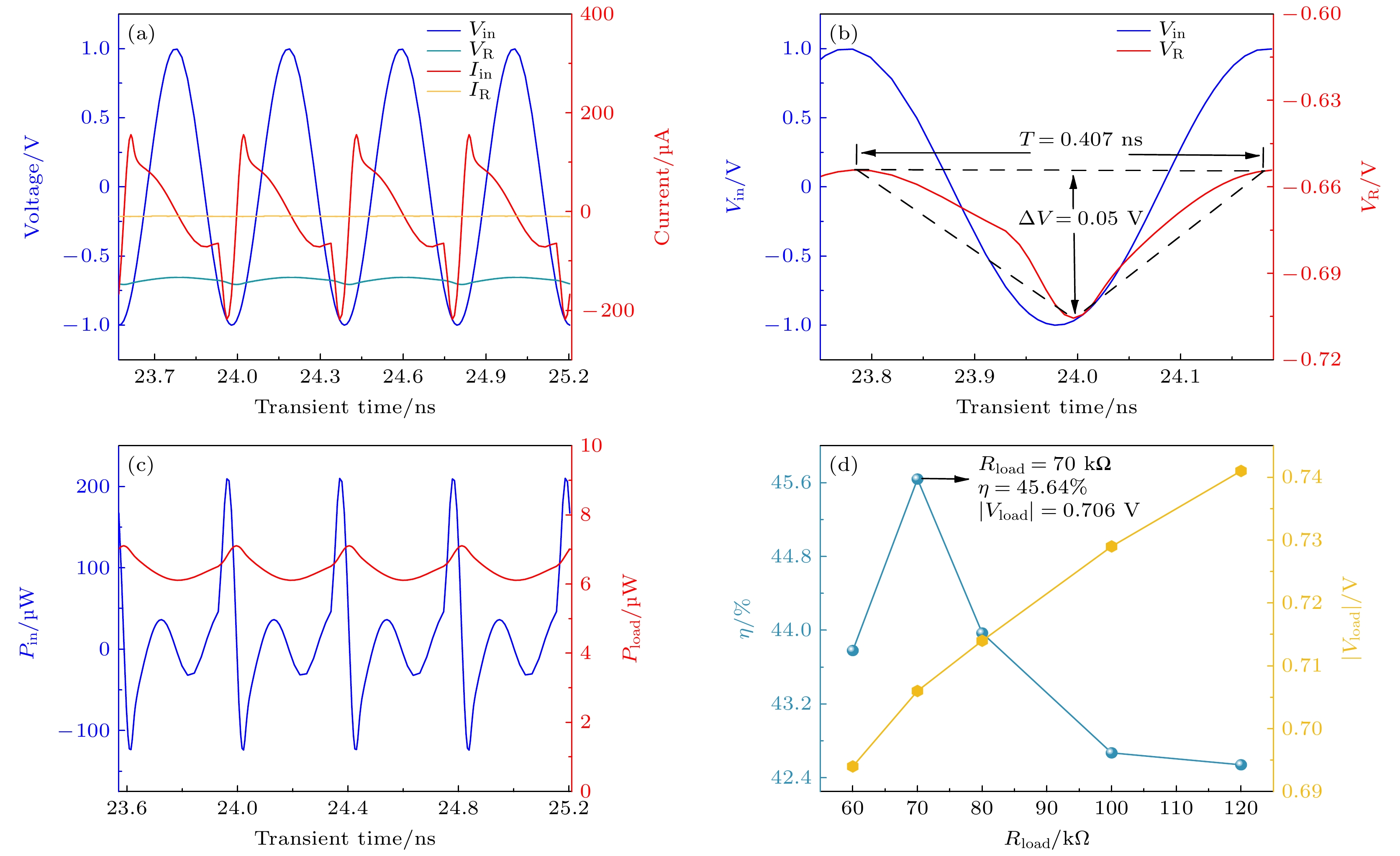
$ \left| {{V_{\text{g}}}} \right| = \left| {{V_{\text{d}}}} \right| = 0 $ ; (b)$ \left| {{V_{\text{g}}}} \right| > \left| {{V_{\text{T}}}} \right| $ .图 13 (a) 瞬态仿真输入输出电流电压波形图; (b) 瞬态仿真输入输出电压单周期局部放大图; (c) 瞬态仿真输入输出功率图; (d) 整流效率和负载电压随负载阻抗变化图
Figure 13. (a) Transient simulation input and output current and voltage waveforms; (b) transient simulation input and output voltage single-cycle partial enlarged diagram; (c) transient simulation input and output power diagrams; (d) rectification efficiency and load voltage with load impedance change graph.
-
[1] Ullah M A, Keshavarz R, Abolhasan M, Lipman J, Esselle K P, Shariati N 2022 IEEE Access 10 17231
 Google Scholar
[2] Haerinia M, Shadid R 2020 Signals 1 209
 Google Scholar
[3] Divakaran S K, Krishna D D 2019 INT. J. RF. Microw. C. E 29 e21633
 Google Scholar
[4] Zhang Z, Pang H, Georgiadis A, Cecati C 2019 IEEE Trans. Ind. Electron. 66 1044
 Google Scholar
[5] Eteng A A, Goh H H, Rahim S K A, Alomainy A 2021 IEEE Access 9 27518
 Google Scholar
[6] Zhu G L, Du J X, Yang X X, Zhou Y G, Gao S 2019 IEEE Access 7 141978
 Google Scholar
[7] Xiao H, Zhang H, Song W, Wang J, Chen W, Lu M 2021 IEEE Trans. Ind. Electron. 69 2896
 Google Scholar
[8] 宋建军, 张龙强, 陈雷, 周亮, 孙雷, 兰军峰, 习楚浩, 李家豪 2021 70 108401
 Google Scholar
Song J J, Zhang L Q, Chen L, Zhou L, Sun L, Lan J F, Xi C H, Li J H 2021 Acta Phys. Sin. 70 108401
 Google Scholar
[9] 李妤晨, 陈航宇, 宋建军 2020 69 108401
 Google Scholar
Li Y C, Chen H Y, Song J J 2020 Acta Phys. Sin. 69 108401
 Google Scholar
[10] Chong G, Ramiah H, Yin J, Rajendran J, Mak P I, Martins R P 2019 IEEE Trans. Circuits Syst. II, Exp. Briefs 68 1743
 Google Scholar
[11] Choi W, Lee J, Shin M 2014 IEEE Trans. Electron Devices 61 37
 Google Scholar
[12] Kim S, Lee K, Lee J H, Park B G, Kwon D 2021 IEEE Trans. Electron Devices 68 4754
 Google Scholar
[13] Yao Y, Sun Y, Li X, Shi Y, Liu Z 2020 IEEE Trans. Electron Devices 67 751
 Google Scholar
[14] Chen C W, Tzeng J Y, Chuang C T, Chien H P, Chien C H, Luo G L 2014 IEEE Trans. Electron Devices 61 2656
 Google Scholar
[15] 张茂添 2014 硕士学位论文 (厦门: 厦门大学)
Zhang M T 2014 M. S. Thesis (Xiamen: Xiamen University) (in Chinese)
[16] 施敏, 伍国珏(耿莉, 张瑞智译) 2007 半导体器件物理 (北京: 西安交通大学出版社) 第 130—142页
Sze S M, Kwok K N (translated by Geng L, Zhang R Z) 2007 Physics of Semiconductor Devices (Xi’an: Xi’an jiaotong University Press) pp130–142 (in Chinese)
[17] 汤晓燕 2007博士学位论文 (西安: 西安电子科技大学)
Tang X Y 2007 Ph. D. Dissertation (Xi’an: Xidian University) (in Chinese)
[18] Shokrani M R, Hamidon M N, Khoddam M, Najafi V 2012 IEEE International Conference on Electronics Design Kuala Lumpur, Malaysia, November 5–6, 2012 p234
[19] Shokrani M R, Khoddam M, Hamidon M N B, Kamsani N A, Rokhani F Z, Shafie S B 2014 Sci. World J. 2014 1
 Google Scholar
[20] Zhang D, Song J J, Xue X H, Zhang S Q 2022 Chin. Phys. B 31 068401
 Google Scholar
Catalog
Metrics
- Abstract views: 7399
- PDF Downloads: 80
- Cited By: 0


 DownLoad:


