


-
Large-area capacitively coupled discharges are widely used in plasma enhanced chemical vapor deposition (PECVD) processes for solar cell and display manufacturing. With the increase of the chamber size and driving frequency for improving production efficiency, the non-uniformity of deposited film induced by standing wave effects becomes more serious, which deserves more attention and in-depth research. Based on a fluid model coupled with a transmission line model, the potential amplitude distribution on the powered 2 m2 electrode and the plasma characteristics in a capacitive plasma sustained in a silane/hydrogen discharge driven at 27.12 MHz are investigated. This work identifies three key control parameters: pressure, silane content, and input power, with particular emphasis on radial wave attenuation caused by electron-neutral elastic collisions. The simulation results are validated by industrial experimental results, confirming the relationship between the distributions of potential amplitude on the powered electrode and the film thickness. Two different mechanisms emerge from the analysis. Under the conditions of low silane content and high power, the surface wave radial attenuation is not significant and the surface wave wavelength variations dominate the potential amplitude distribution on the powered electrode. Conversely, in the case of high silane content and low power, significant radial attenuation of the surface wave leads to the noticeable weakening of the standing wave effect due to higher electron-neutral collision frequency. Neglecting the radial attenuation of the surface wave will result in significant deviations in the potential amplitude distribution on the powered electrode as shown in the following figure. Strategies such as adjusting power input positions or using multiple power input are studied to improve uniformity, but the improvements are still limited. Although it requires strict parameter control and machining precision, the shaped electrode demonstrates remarkable uniformity improvement of the potential distribution. In the future work, it is necessary to further analyze the influence of the standing wave effects on the radial distributions of electron, ions, and neutral radicals under complex conditions, such as different chamber structures, gas flows, and temperature distributions, as well as the influence on the quality of deposited films. This will enable a more comprehensive and accurate study of standing wave effects, providing support and guidance for solving real industrial problems. 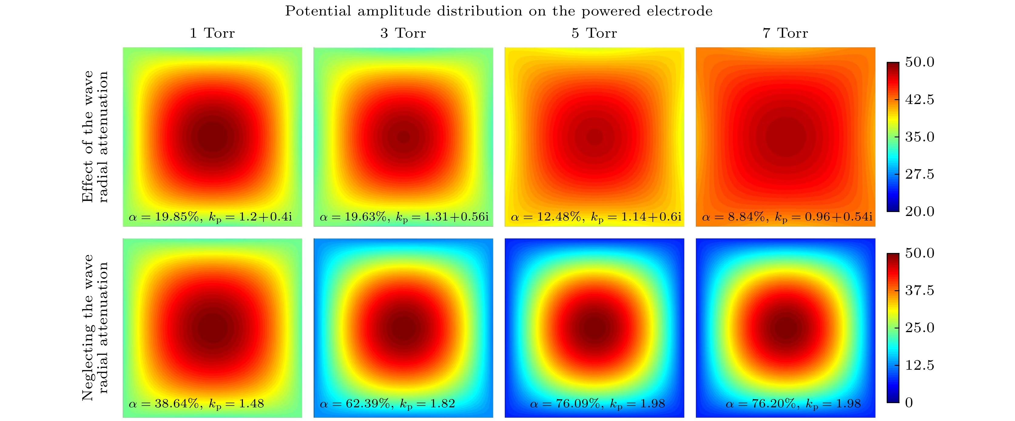
-
Keywords:
- capacitive coupling discharge /
- plasma enhanced chemical vapor deposition /
- standing wave effect
[1] Yu C, Gao K, Peng C W, He C R, Wang S B, Shi W, Allen V, Zhang J T, Wang D Z, Tian G Y, Zhang Y F, Jia W Z, Song Y H, Hu Y Z, Colwell J, Xing C F, Ma Q, Wu H T, Guo L Y, Dong G Q, Jiang H, Wu H H, Wang X Y, Xu D C, Li K, Peng J, Liu W Z, Chen D, Lennon A, Cao X M, De Wolf S, Zhou J, Yang X B, Zhang X H 2023 Nat. Energy 8 1375
 Google Scholar
[2] Crose M, Kwon J S I, Tran A, Christofides P D 2017 Renewable Energy 100 129
Google Scholar
[3] Crose M, Sang Il Kwon J, Nayhouse M, Ni D, Christofides P D 2015 Chem. Eng. Sci. 136 50
Google Scholar
[4] Schmidt H 2006 Ph. D Dissertation (Lausanne: EPFL
[5] Schmitt J P M 1989 Thin Solid Films 174 193
Google Scholar
[6] Meyyappan M, Colgan M J 1996 J. Vac. Sci. Technol. A 14 2790
Google Scholar
[7] Surendra M, Graves D B 1991 Appl. Phys. Lett 59 2091
Google Scholar
[8] Curtins H, Wyrsch N, Favre M, Shah A V 1987 Plasma Chem Plasma P 7 267
Google Scholar
[9] Liu Y X, Zhang Q Z, Zhao K, Zhang Y R, Gao F, Song Y H, Wang Y N 2022 Chin. Phys. B 31 085202
Google Scholar
[10] Kim H J, Lee H J 2017 J. Phys. D: Appl. Phys. 122 053301
Google Scholar
[11] Kim H J, Lee H J 2017 Plasma Sources Sci. Technol. 26 085003
Google Scholar
[12] Kim H J 2021 Vacuum 187 110104
Google Scholar
[13] Kim H J, Lee H J 2016 Plasma Sources Sci. Technol. 25 065006
Google Scholar
[14] Schmidt H, Sansonnens L, Howling A A, Hollenstein Ch, Elyaakoubi M, Schmitt J P M 2004 J. Appl. Phys. 95 4559
Google Scholar
[15] Sansonnens L, Pletzer A, Magni D, Howling A A, Hollenstein C, Schmitt J P M 1997 Plasma Sources Sci. Technol. 6 170
Google Scholar
[16] Lieberman M A, Booth J P, Chabert P, Rax J M, Turner M M 2002 Plasma Sources Sci. Technol. 11 283
Google Scholar
[17] Chabert P, Raimbault J L, Rax J M, Lieberman M A 2004 Phys. Plasmas 11 1775
Google Scholar
[18] Lee I, Graves D B, Lieberman M A 2008 Plasma Sources Sci. Technol. 17 015018
Google Scholar
[19] Lieberman M A, Lichtenberg A J, Kawamura E, Marakhtanov A M 2015 Plasma Sources Sci. Technol. 24 055011
Google Scholar
[20] Wen D Q, Kawamura E, Lieberman M A, Lichtenberg A J, Wang Y N 2017 J. Phys. D: Appl. Phys. 50 495201
Google Scholar
[21] Zhao K, Liu Y X, Kawamura E, Wen D Q, Lieberman M A, Wang Y N 2018 Plasma Sources Sci. Technol. 27 055017
Google Scholar
[22] Lieberman M A, Kawamura E, Chabert P 2022 Plasma Sources Sci. Technol. 31 114007
Google Scholar
[23] Liu J K, Zhang Y R, Zhao K, Wen D Q, Wang Y N 2021 Plasma Sci. Technol. 23 035401
Google Scholar
[24] Liu Y X, Gao F, Liu J, Wang Y N 2014 J. Appl. Phys. 116 043303
Google Scholar
[25] Han D M, Liu Y X, Gao F, Wang X Y, Li A, Xu J, Jing Z G, Wang Y N 2018 J. Appl. Phys. 123 223304
Google Scholar
[26] Han D M, Su Z X, Zhao K, Liu Y X, Gao F, Wang Y N 2021 Plasma Sci. Technol. 23 055402
Google Scholar
[27] Sansonnens L, Schmidt H, Howling A A, Hollenstein Ch, Ellert Ch, Buechel A 2006 J. Vac. Sci. Technol. A 24 1425
Google Scholar
[28] Chen Z, Rauf S, Collins K 2010 J. Appl. Phys. 108 073301
Google Scholar
[29] Faraz T, Arts K, Karwal S, Knoops H C M, Kessels W M M 2019 Plasma Sources Sci. Technol. 28 024002
Google Scholar
[30] Kuboi N 2023 J. Micro/Nanopattern. Mats. Metro. 22 041502
Google Scholar
[31] Oehrlein G S, Brandstadter S M, Bruce R L, et al. 2024 J. Vac. Sci. Technol. B 42 041501
Google Scholar
[32] Chang J, Chang J P 2017 J. Phys. D: Appl. Phys. 50 253001
Google Scholar
[33] 邱华檀, 王友年, 马腾才 2002 51 1332
Google Scholar
Qiu H T, Wang Y N, Ma T C 2002 Acta Phys. Sin. 51 1332
Google Scholar
[34] Tinck S, Bogaerts A 2012 Plasma Processes & Polym. 9 522
Google Scholar
[35] Kessels W M M, Hoefnagels J P M, Boogaarts M G H, Schram D C, Van De Sanden M C M 2001 J. Appl. Phys. 89 2065
Google Scholar
[36] 刘建凯 2022 博士学位论文(大连: 大连理工大学)
Liu J K 2022 Ph. D Dissertation (Dalian: Dalian University of Technology
[37] Sansonnens L 2005 J. Appl. Phys. 97 063304
Google Scholar
[38] Jia W Z, Wang X F, Song Y H, Wang Y N 2017 J. Phys. D: Appl. Phys. 50 165206
Google Scholar
[39] Jia W Z, Liu R Q, Wang X F, Liu X M, Song Y H, Wang Y N 2018 Phys. Plasmas 25 093501
Google Scholar
[40] Bleecker K D, Bogaerts A, Gijbels R, Goedheer W 2004 Phys. Rev. E 69 056409
Google Scholar
[41] Brinkmann R P 2007 J. Appl. Phys. 102 093303
Google Scholar
-
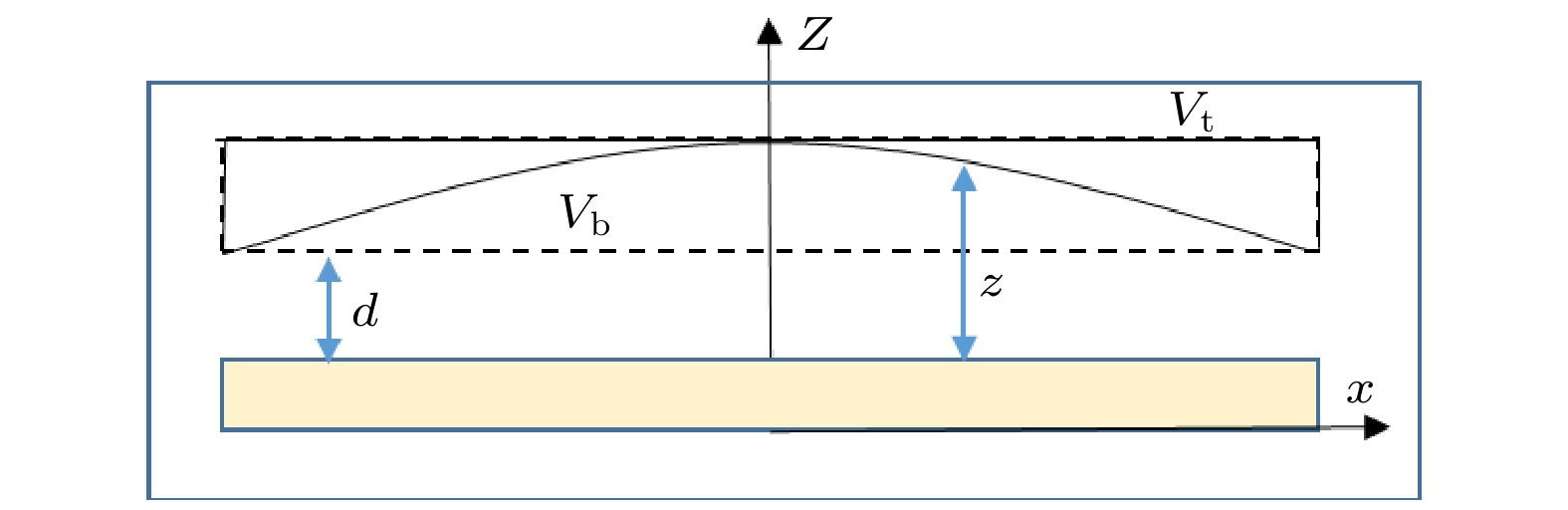
图 1 腔室结构示意图
Figure 1. Diagram of chamber structure.
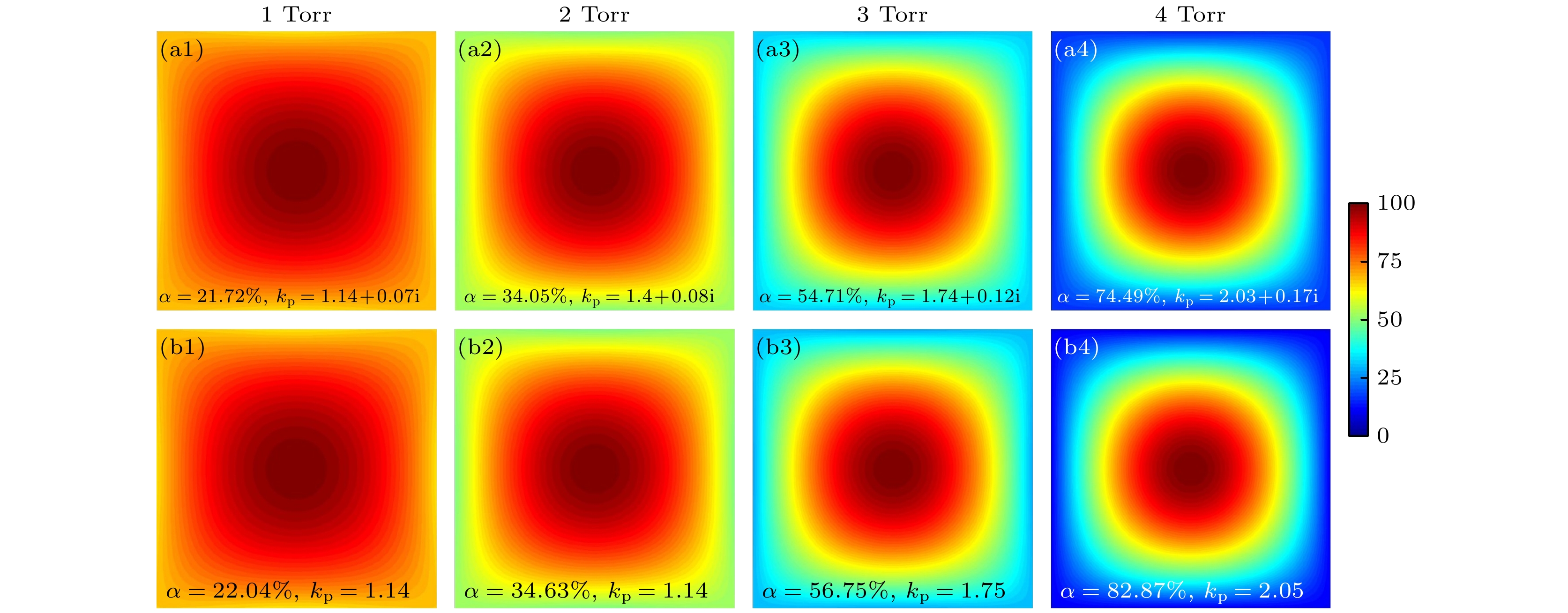
图 2 不同气压下的考虑(a1)—(a4)和忽略(b1)—(b4)表面波径向衰减情况下的驱动电极电势幅值的二维分布(以下简称电势分布)以及每种情况下的电势分布不均匀度$ \alpha $和表面波波数$ {k}_{{\mathrm{p}}} $, 电极尺寸为2 m × 2 m, 其他放电条件与表2相同
Figure 2. Two-dimensional distributions of the potential amplitude on the powered electrode with (a1)–(a4) or without (b1)–(b4) the consideration of the surface wave radial attenuation under different pressures, with the potential nonuniformity factor $ \alpha $ and surface wave number $ {k}_{{\mathrm{p}}} $ for each case. Electrode size: 2 m × 2 m; other discharge conditions are the same as in Table 2.
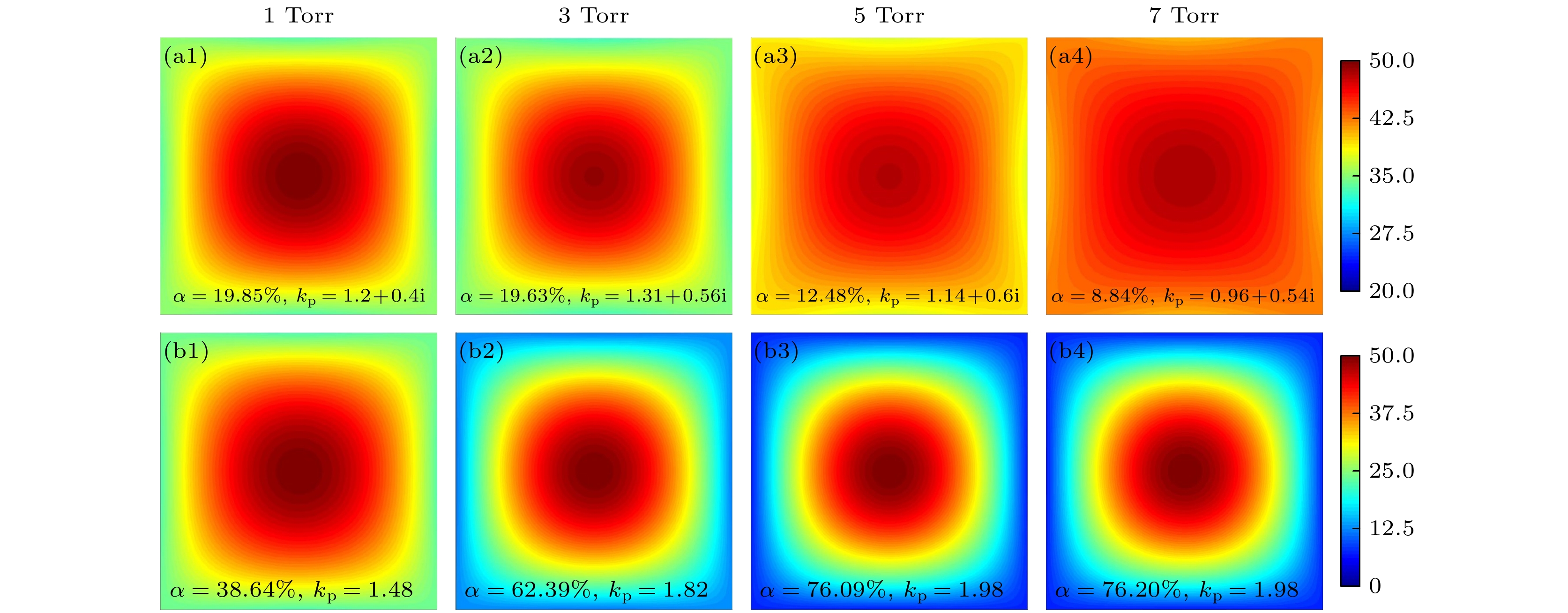
图 3 不同气压下的考虑(a1)—(a4)和忽略(b1)—(b4)表面波径向衰减情况下的电势分布以及每种情况下的电势分布不均匀度$ \alpha $和表面波波数$ {k}_{{\mathrm{p}}} $. 电极尺寸为2 m × 2 m; 其他放电条件与表3相同
Figure 3. Distributions of the potential with (a1)–(a4) or without (b1)–(b4) the consideration of the surface wave radial attenuation under different pressures, with the potential nonuniformity factor $ \alpha $ and surface wave number $ {k}_{{\mathrm{p}}} $ for each case. Electrode size is 2 m × 2 m; other discharge conditions are the same as in Table 3.
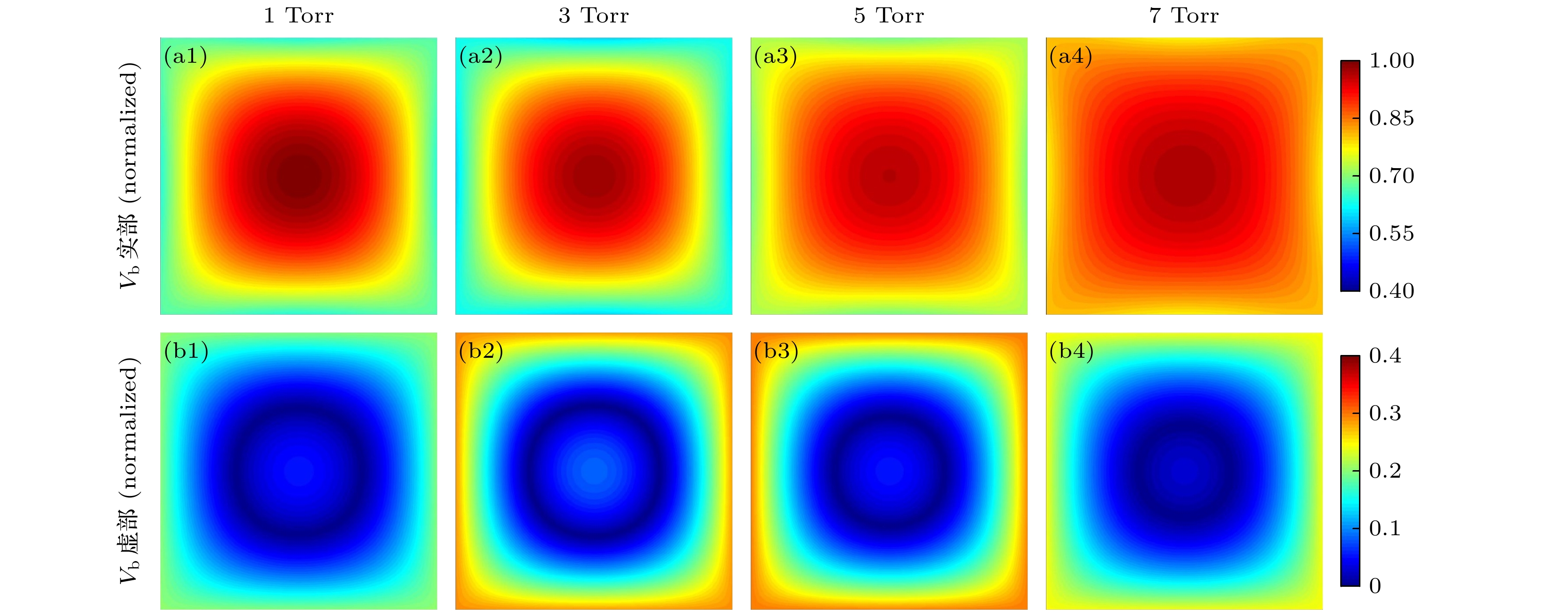
图 4 不同气压下考虑表面波径向衰减时归一化的电势分布的实部(a1)—(a4)和虚部(b1)—(b4). 电极尺寸为2 m × 2 m; 其他放电条件与表3相同
Figure 4. Distributions of the real part (a1)–(a4) and imaginary part (b1)–(b4) of the normalized potential with the consideration of the surface wave radial attenuation. Electrode size is 2 m × 2 m; other discharge conditions are the same as in Table 3.
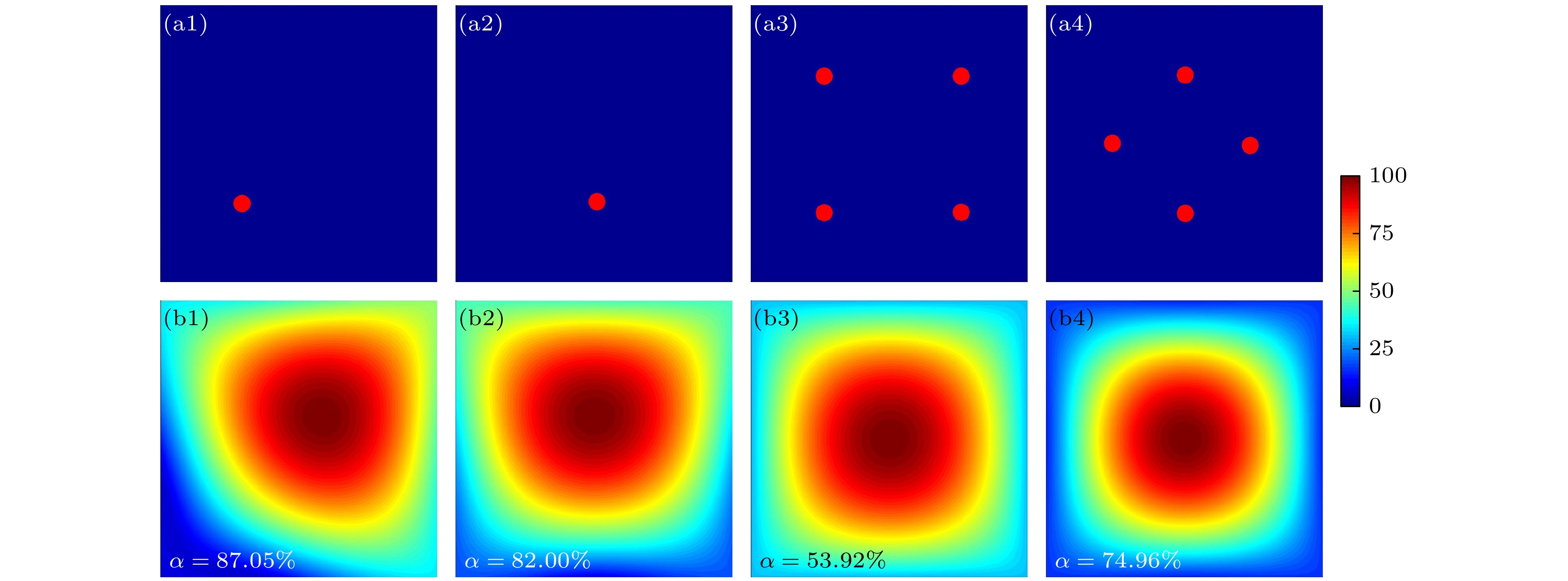
图 5 不同案例下电源馈入位置示意图(a1)—(a4)和对应的电势分布(b1)—(b4)以及电势分布不均匀度$ \alpha $. 电极尺寸为2 m × 2 m; 放电气压为3 Torr; 其他放电条件与表2相同
Figure 5. Distributions of power input positions (a1)–(a4) under different cases, and the potential (b1)–(b4), as well as the potential nonuniformity factor α. Electrode size is 2 m × 2 m; pressure is 3 Torr; other discharge conditions are the same as in Table 2.

图 6 不同气压下采用图5(a1)馈入方式模拟计算的电势分布(a), (c)和相同条件下实验观测的沉积薄膜厚度分布(b), (d). 模拟与实验放电参数相同, 电极尺寸为2 m × 2 m; 其他放电条件与表2相同
Figure 6. Distributions of the potential from simulation (a), (c) and the deposited film thickness from experiment (b), (d) under different pressures with the case of power input in Fig. 5(a1). Discharge parameters of simulation and experiment are consistent, electrode size is 2 m × 2 m; other discharge conditions are the same as in Table 2.
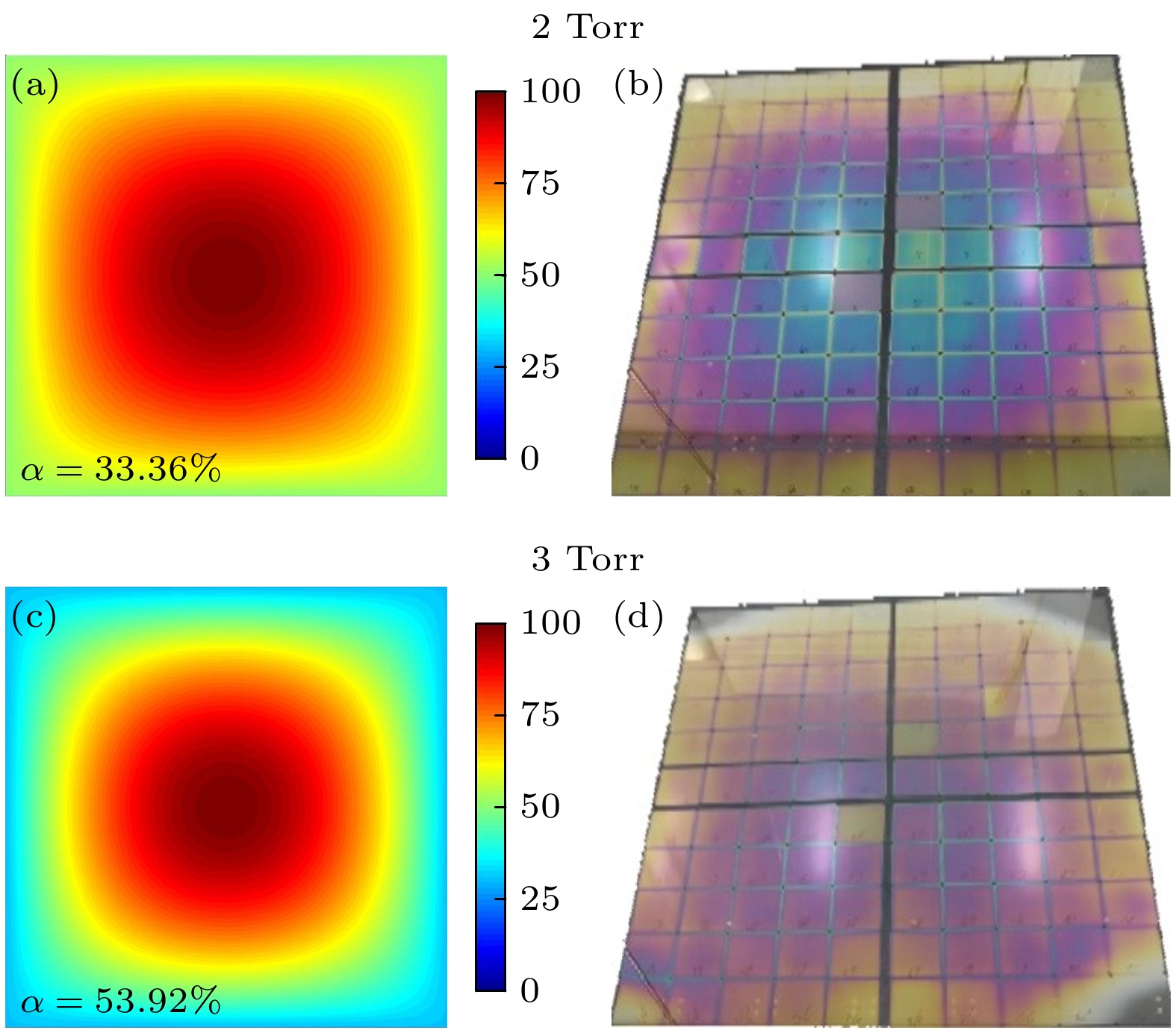
图 7 不同气压下采用图5(a3)馈入方式模拟计算的电势分布(a), (c)和相同条件下实验观测的沉积薄膜厚度分布(b), (d). 模拟与实验放电参数相同, 电极尺寸为2 m × 2 m; 其他放电条件与表2相同
Figure 7. Distributions of the potential from simulation (a), (c) and the deposited film thickness from experiment (b), (d) under different pressures with the case of power input in Fig. 5(a1). Discharge parameters of simulation and experiment are consistent, electrode size is 2 m × 2 m; other discharge conditions are the same as in Table 2.
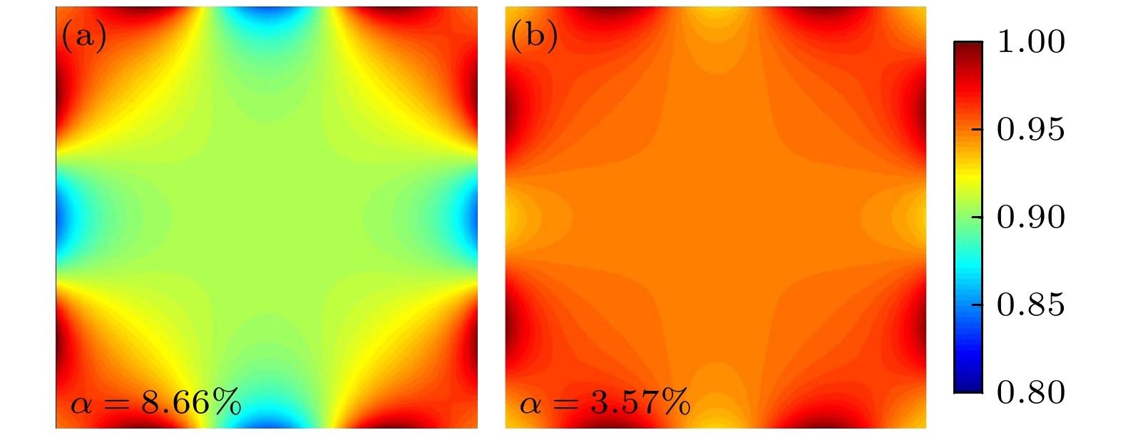
图 8 采用曲面电极和图5(a3)馈入方式情况下放电区域归一化的电势分布. 电极尺寸为2 m × 2 m; 放电气压为 4 Torr; 其他放电条件与表2相同
Figure 8. Distributions of the normalized potential with the shaped electrode and the case of power input in Fig. 5(a3). Electrode size is 2 m × 2 m; pressure is 4 Torr; other discharge conditions are the same as in Table 2.
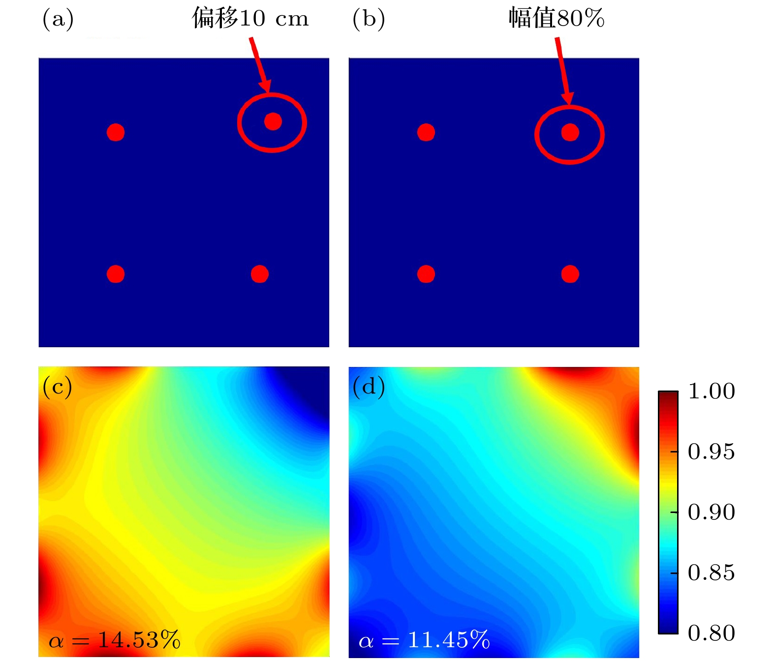
图 9 采用曲面电极和图5(a3)馈入方式情况下, 当右上角电源偏离理想位置(a)和电源电流幅值偏离理想值(b)时归一化的电势分布(c), (d). 电极尺寸为2 m × 2 m; 放电气压为 4 Torr; 其他放电条件与表2相同
Figure 9. Distributions of the normalized potential (c), (d) when the power input position deviates from the ideal position (a) or the current amplitude deviates from the ideal value (b) with the shaped electrode and the case of power input in Fig. 5(a3). Electrode size is 2 m × 2 m; pressure is 4 Torr; other discharge conditions are the same as in Table 2.
表 1 流体模型中计算硅烷氢气放电的反应及其系数
Table 1. Reactions and corresponding coefficients in fluid models for silane/hydrogen discharges.
序号 反应 阈值能/eV 系数[38,39]
/(cm3·s–1)R1 SiH4+e→SiH4+e — cal R2 SiH4+e→$ {{\mathrm{S}}{\mathrm{i}}{\mathrm{H}}}_{3}^{+} $+H+2e 11.9 cal R3 SiH4+e→$ {{\mathrm{S}}{\mathrm{i}}{\mathrm{H}}}_{3}^{-} $+H 5.7 cal R4 SiH4+e→$ {{\mathrm{S}}{\mathrm{i}}{\mathrm{H}}}_{2}^{-} $+2H 5.7 cal R5 SiH4+e→SiH3+H+e 8.3 cal R6 SiH4+e→SiH2+2H+e 8.3 cal R7 H2+e→H2+e — cal R8 H2+e→2H+e 8.9 cal R9 H2+e→$ {{\mathrm{H}}}_{2}^{+} $+2e 15.4 cal R10 Si2H6+e→Si2$ {{\mathrm{H}}}_{4}^{+} $+2H+2e 10.2 cal R11 Si2H6+e→SiH3+SiH2+H+e 7.0 cal R12 $ {{\mathrm{S}}{\mathrm{i}}{\mathrm{H}}}_{3}^{+} $+ $ {{\mathrm{S}}{\mathrm{i}}{\mathrm{H}}}_{3}^{-} $→2SiH3 — 1.0×10⁻⁸ R13 $ {{\mathrm{S}}{\mathrm{i}}{\mathrm{H}}}_{3}^{+} $+$ {{\mathrm{S}}{\mathrm{i}}{\mathrm{H}}}_{2}^{-} $→SiH3+SiH2 — 1.0×10⁻⁸ R14 $ {{\mathrm{H}}}_{2}^{+} $+$ {{\mathrm{S}}{\mathrm{i}}{\mathrm{H}}}_{3}^{-} $→SiH3+H2 — 1.0×10⁻⁸ R15 $ {{\mathrm{H}}}_{2}^{+} $+$ {{\mathrm{S}}{\mathrm{i}}{\mathrm{H}}}_{2}^{-} $→SiH2+H2 — 1.0×10⁻⁸ R16 Si2$ {{\mathrm{H}}}_{4}^{+} $+$ {{\mathrm{S}}{\mathrm{i}}{\mathrm{H}}}_{3}^{-} $→SiH3+H2 — 1.0×10⁻⁸ R17 Si2$ {{\mathrm{H}}}_{4}^{+} $+$ {{\mathrm{S}}{\mathrm{i}}{\mathrm{H}}}_{2}^{-} $→3SiH2 — 1.0×10⁻⁸ R18 SiH4+$ {{\mathrm{H}}}_{2}^{+} $→$ {{\mathrm{S}}{\mathrm{i}}{\mathrm{H}}}_{3}^{+} $+H2+H — 1.0×10⁻⁸ R19 SiH4+H→SiH3+H2 — 1.2×10⁻¹² R20 Si2H6+H→H2+Si2H5 — 7.0×10⁻¹² R21 Si2H6+H→SiH3+SiH4 — 3.5×10⁻¹² R22 SiH3+SiH3→SiH4+SiH2 — 1.5×10⁻¹⁰ R23 SiH2+H2→SiH4 — 2.7×10⁻¹⁴ R24 SiH2+SiH4→Si2H6 — 2.3×10⁻¹¹  DownLoad: CSV
表 2 不同气压下周期和空间平均的电子密度($ {n}_{{\mathrm{e}}} $)、鞘层厚度($ {d}_{{\mathrm{s}}{\mathrm{h}}} $)、趋肤深度($ \delta $)、电子-中性粒子弹性碰撞频率($ {\upsilon }_{{\mathrm{e}}{\mathrm{n}}} $)和电极间有效相对介电常数($ {\varepsilon }_{{\mathrm{e}}{\mathrm{f}}{\mathrm{f}}} $); 放电条件为电压幅值100 V, 间距1.6 cm, 功率范围8—12 kW, SiH4/SiH4+H2 = 1%
Table 2. Periodically and spatially averaged electron density ($ {n}_{{\mathrm{e}}} $), sheath thickness ($ {d}_{{\mathrm{s}}{\mathrm{h}}} $), skin depth ($ \delta $), electron-neutral elastic collision frequency ($ {\upsilon }_{{\mathrm{e}}{\mathrm{n}}} $), and effective relative permittivity ($ {\varepsilon }_{{\mathrm{e}}{\mathrm{f}}{\mathrm{f}}} $) under different pressures; discharge conditions: voltage 100 V, gap 1.6 cm, power range 8–12 kW, SiH4/SiH4+H2 = 1%.
p/Torr $ {n}_{{\mathrm{e}}} $/(1015 m–3) $ {d}_{{\mathrm{s}}{\mathrm{h}}} $/cm $ \boldsymbol{\delta } $/cm $ {\upsilon }_{{\mathrm{e}}{\mathrm{n}}} $/(1010Hz) $ {\varepsilon }_{{\mathrm{e}}{\mathrm{f}}{\mathrm{f}}} $ 1 5.98 0.20 6.88 0.36 4.02+0.46i 2 19.56 0.13 3.80 0.72 6.08+0.68i 3 37.57 0.08 2.74 1.08 9.30+1.29i 4 55.81 0.06 2.25 1.44 12.65+2.20i
DownLoad: CSV
表 3 不同气压下周期和空间平均的电子密度($ {n}_{{\mathrm{e}}} $)、鞘层厚度($ {d}_{{\mathrm{s}}{\mathrm{h}}} $)、趋肤深度($ \delta $)、电子-中性粒子弹性碰撞频率($ {\upsilon }_{{\mathrm{e}}{\mathrm{n}}} $)和电极间相对介电常数($ {\varepsilon }_{{\mathrm{e}}{\mathrm{f}}{\mathrm{f}}} $), 放电条件为电压幅值50 V, 间距2 cm, 功率大致2—5 kW, SiH4/SiH4+H2 = 90%
Table 3. Periodically and spatially electron density ($ {n}_{{\mathrm{e}}} $), sheath thickness ($ {d}_{{\mathrm{s}}{\mathrm{h}}} $), skin depth ($ \delta $), electron-neutral elastic collision frequency ($ {\upsilon }_{{\mathrm{e}}{\mathrm{n}}} $), and effective relative permittivity ($ {\varepsilon }_{{\mathrm{e}}{\mathrm{f}}{\mathrm{f}}} $) under different pressures, discharge conditions: voltage 50 V, gap 2 cm, power range 2–5 kW, SiH4/SiH4+H2 = 90%.
p/Torr $ {n}_{{\mathrm{e}}} $/(1015 m–3) $ {d}_{{\mathrm{s}}{\mathrm{h}}} $/cm ${\delta } $/cm $ {\upsilon }_{{\mathrm{e}}{\mathrm{n}}} $/(1010 Hz) $ {\varepsilon }_{{\mathrm{e}}{\mathrm{f}}{\mathrm{f}}} $ 1 2.40 0.15 10.86 0.59 3.99+3.02i 3 7.72 0.10 6.06 1.77 4.33+4.53i 5 9.12 0.08 5.57 2.94 2.88+4.25i 7 8.70 0.08 5.70 4.12 1.94+3.18i
DownLoad: CSV
-
[1] Yu C, Gao K, Peng C W, He C R, Wang S B, Shi W, Allen V, Zhang J T, Wang D Z, Tian G Y, Zhang Y F, Jia W Z, Song Y H, Hu Y Z, Colwell J, Xing C F, Ma Q, Wu H T, Guo L Y, Dong G Q, Jiang H, Wu H H, Wang X Y, Xu D C, Li K, Peng J, Liu W Z, Chen D, Lennon A, Cao X M, De Wolf S, Zhou J, Yang X B, Zhang X H 2023 Nat. Energy 8 1375
Google Scholar
[2] Crose M, Kwon J S I, Tran A, Christofides P D 2017 Renewable Energy 100 129
Google Scholar
[3] Crose M, Sang Il Kwon J, Nayhouse M, Ni D, Christofides P D 2015 Chem. Eng. Sci. 136 50
Google Scholar
[4] Schmidt H 2006 Ph. D Dissertation (Lausanne: EPFL
[5] Schmitt J P M 1989 Thin Solid Films 174 193
Google Scholar
[6] Meyyappan M, Colgan M J 1996 J. Vac. Sci. Technol. A 14 2790
Google Scholar
[7] Surendra M, Graves D B 1991 Appl. Phys. Lett 59 2091
Google Scholar
[8] Curtins H, Wyrsch N, Favre M, Shah A V 1987 Plasma Chem Plasma P 7 267
Google Scholar
[9] Liu Y X, Zhang Q Z, Zhao K, Zhang Y R, Gao F, Song Y H, Wang Y N 2022 Chin. Phys. B 31 085202
Google Scholar
[10] Kim H J, Lee H J 2017 J. Phys. D: Appl. Phys. 122 053301
Google Scholar
[11] Kim H J, Lee H J 2017 Plasma Sources Sci. Technol. 26 085003
Google Scholar
[12] Kim H J 2021 Vacuum 187 110104
Google Scholar
[13] Kim H J, Lee H J 2016 Plasma Sources Sci. Technol. 25 065006
Google Scholar
[14] Schmidt H, Sansonnens L, Howling A A, Hollenstein Ch, Elyaakoubi M, Schmitt J P M 2004 J. Appl. Phys. 95 4559
Google Scholar
[15] Sansonnens L, Pletzer A, Magni D, Howling A A, Hollenstein C, Schmitt J P M 1997 Plasma Sources Sci. Technol. 6 170
Google Scholar
[16] Lieberman M A, Booth J P, Chabert P, Rax J M, Turner M M 2002 Plasma Sources Sci. Technol. 11 283
Google Scholar
[17] Chabert P, Raimbault J L, Rax J M, Lieberman M A 2004 Phys. Plasmas 11 1775
Google Scholar
[18] Lee I, Graves D B, Lieberman M A 2008 Plasma Sources Sci. Technol. 17 015018
Google Scholar
[19] Lieberman M A, Lichtenberg A J, Kawamura E, Marakhtanov A M 2015 Plasma Sources Sci. Technol. 24 055011
Google Scholar
[20] Wen D Q, Kawamura E, Lieberman M A, Lichtenberg A J, Wang Y N 2017 J. Phys. D: Appl. Phys. 50 495201
Google Scholar
[21] Zhao K, Liu Y X, Kawamura E, Wen D Q, Lieberman M A, Wang Y N 2018 Plasma Sources Sci. Technol. 27 055017
Google Scholar
[22] Lieberman M A, Kawamura E, Chabert P 2022 Plasma Sources Sci. Technol. 31 114007
Google Scholar
[23] Liu J K, Zhang Y R, Zhao K, Wen D Q, Wang Y N 2021 Plasma Sci. Technol. 23 035401
Google Scholar
[24] Liu Y X, Gao F, Liu J, Wang Y N 2014 J. Appl. Phys. 116 043303
Google Scholar
[25] Han D M, Liu Y X, Gao F, Wang X Y, Li A, Xu J, Jing Z G, Wang Y N 2018 J. Appl. Phys. 123 223304
Google Scholar
[26] Han D M, Su Z X, Zhao K, Liu Y X, Gao F, Wang Y N 2021 Plasma Sci. Technol. 23 055402
Google Scholar
[27] Sansonnens L, Schmidt H, Howling A A, Hollenstein Ch, Ellert Ch, Buechel A 2006 J. Vac. Sci. Technol. A 24 1425
Google Scholar
[28] Chen Z, Rauf S, Collins K 2010 J. Appl. Phys. 108 073301
Google Scholar
[29] Faraz T, Arts K, Karwal S, Knoops H C M, Kessels W M M 2019 Plasma Sources Sci. Technol. 28 024002
Google Scholar
[30] Kuboi N 2023 J. Micro/Nanopattern. Mats. Metro. 22 041502
Google Scholar
[31] Oehrlein G S, Brandstadter S M, Bruce R L, et al. 2024 J. Vac. Sci. Technol. B 42 041501
Google Scholar
[32] Chang J, Chang J P 2017 J. Phys. D: Appl. Phys. 50 253001
Google Scholar
[33] 邱华檀, 王友年, 马腾才 2002 51 1332
Google Scholar
Qiu H T, Wang Y N, Ma T C 2002 Acta Phys. Sin. 51 1332
Google Scholar
[34] Tinck S, Bogaerts A 2012 Plasma Processes & Polym. 9 522
Google Scholar
[35] Kessels W M M, Hoefnagels J P M, Boogaarts M G H, Schram D C, Van De Sanden M C M 2001 J. Appl. Phys. 89 2065
Google Scholar
[36] 刘建凯 2022 博士学位论文(大连: 大连理工大学)
Liu J K 2022 Ph. D Dissertation (Dalian: Dalian University of Technology
[37] Sansonnens L 2005 J. Appl. Phys. 97 063304
Google Scholar
[38] Jia W Z, Wang X F, Song Y H, Wang Y N 2017 J. Phys. D: Appl. Phys. 50 165206
Google Scholar
[39] Jia W Z, Liu R Q, Wang X F, Liu X M, Song Y H, Wang Y N 2018 Phys. Plasmas 25 093501
Google Scholar
[40] Bleecker K D, Bogaerts A, Gijbels R, Goedheer W 2004 Phys. Rev. E 69 056409
Google Scholar
[41] Brinkmann R P 2007 J. Appl. Phys. 102 093303
Google Scholar


 DownLoad:


Catalog
Metrics
- Abstract views: 323
- PDF Downloads: 14
- Cited By: 0
