-
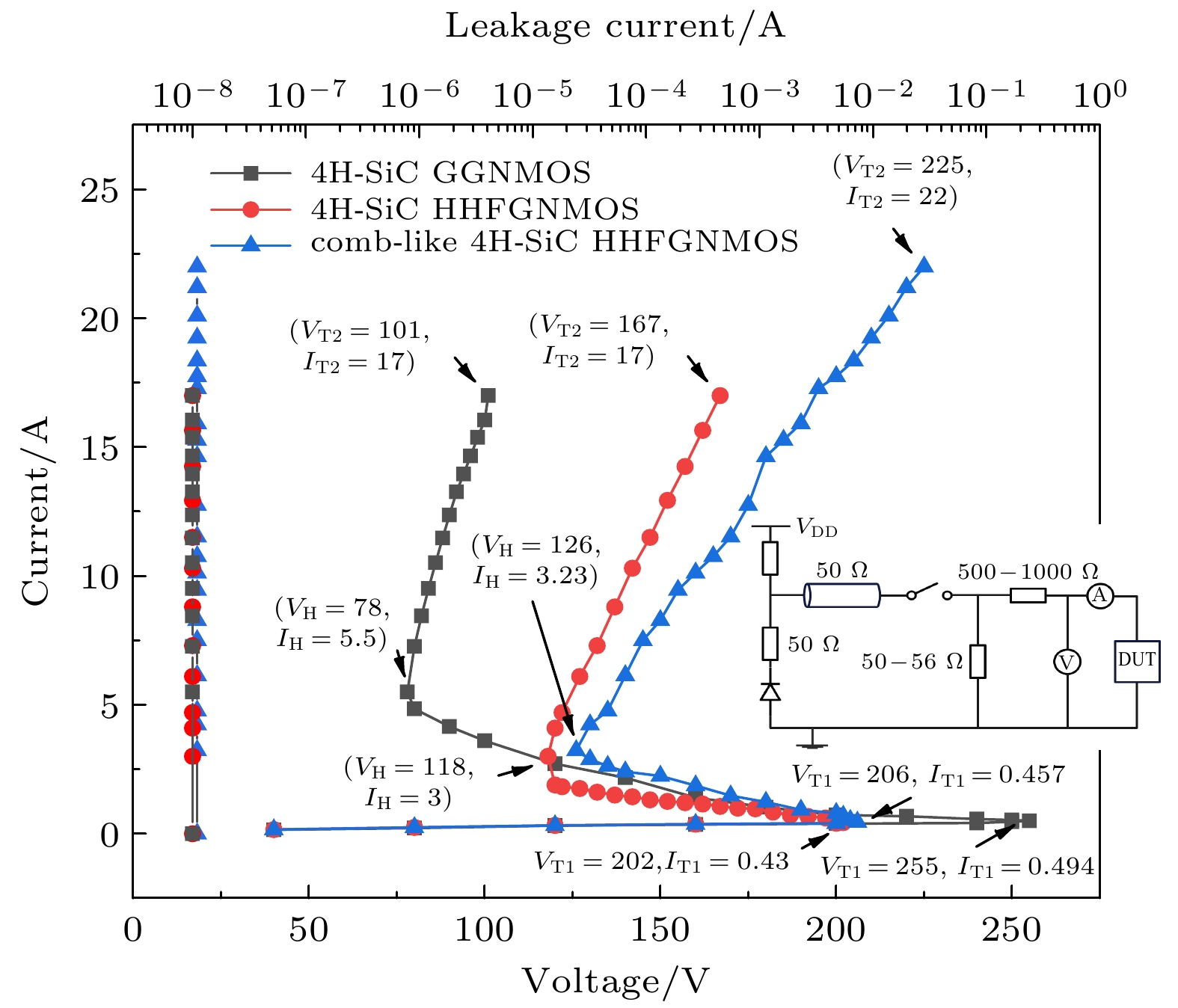
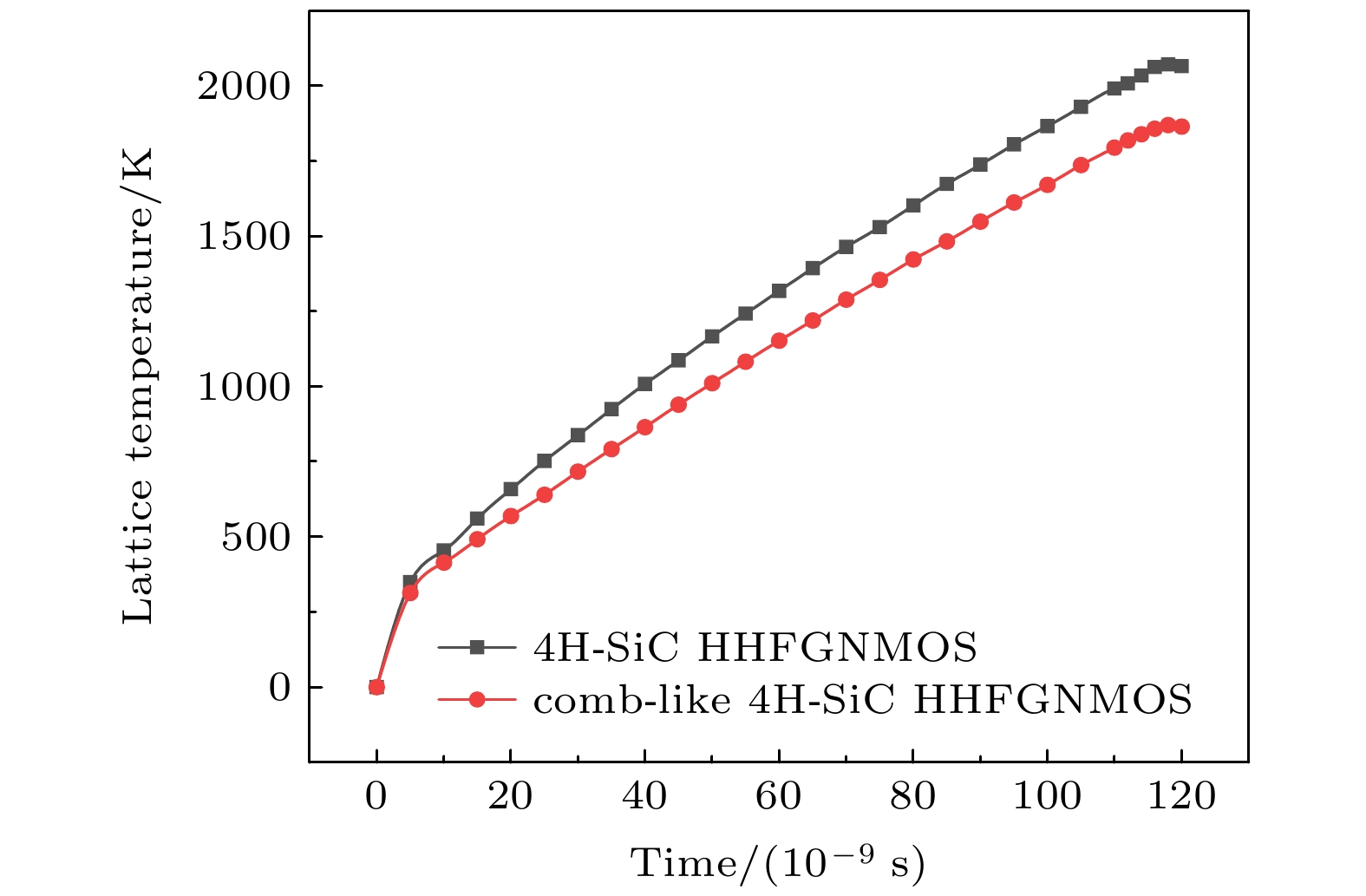
In 2020, Korean scholars proposed a new electrotatic discharge (ESD) protection device HHFGNMOS(high holding voltage floating gate nMOSFET) based on 4H-SiC material, which can significantly improve the severe snapback phenomenon of 4H-SiC GGNMOS due to the characteristics of SiC material. However, there still exists a problem that the current distribution is too dense in the HHFGNMOS structure. In this work, the comb-like structure is used for the HHFGNMOS protection device for the first time. The bottom of the drain region of the device is comb transformed, and the current distribution is made uniform by making full use of the current edge effect. The influence of design variables of comb-like structure on structure performance is given by TCAD simulation. The transient simulation results of GGNMOS, HHFGNMOS and comb-like HHFGNMOS based on 4H-SiC under TLP pulse show that the secondary failure current IT2 of comb-like HHFGNMOS increases from 17 to 22 A i.e. by 29%, compared with that of GGNMOS and HHFGNMOS. In addition, the comb-like HHFGNMOS snapback is reduced by 55.2% and 5% compared with GGNMOS snapback and HHFGNMOS snapback, respectively. Therefore, the robustness of the device is greatly improved and the snapback effect is reduced under the condition of constant area and compatible process.
-
Keywords:
- HHFGNMOS /
- comb-like HHFGNMOS /
- 4H-SiC /
- current density distribution
[1] Ameraskera A, Duvvury C 2002 ESD in silicon integrated circuits (2nd Ed.) (New York: John Wiley & Sons) pp56–341
[2] Wei J, Liu S, Zhang X, Sun W, Huang A Q 2020 IEEE Trans. Power Electron 35 11299
 Google Scholar
[3] Do K I, Won J I, Koo Y S 2020 IEEE Trans. Power Electron 36 4921
 Google Scholar
[4] Do K I, Lee B S, Koo Y S 2018 IEEE Electron Device Lett 40 283
 Google Scholar
[5] Duvvury C, Diaz C H 1992 Reliability Physics Symposium 1992 30th Annual Proceedings., International San Diego, CA, USA, March 31–April 2, 1992 141
[6] Ker M D, Chen T Y 2003 IEEE Trans. Electron. Dev. 50 1050
 Google Scholar
[7] Won J I, Jung J W, Yang I S, Koo Y S 2011 Electron. Lett. 47 1072
 Google Scholar
[8] Lin H S, Shi L C 2002 Chin. J. Electron. 25 209
[9] Wang A Z H 2002 On-Chip ESD Protection for Integrated Circuits: An IC Design Perspective (Kluwer Academic Publishers) pp24–26
-
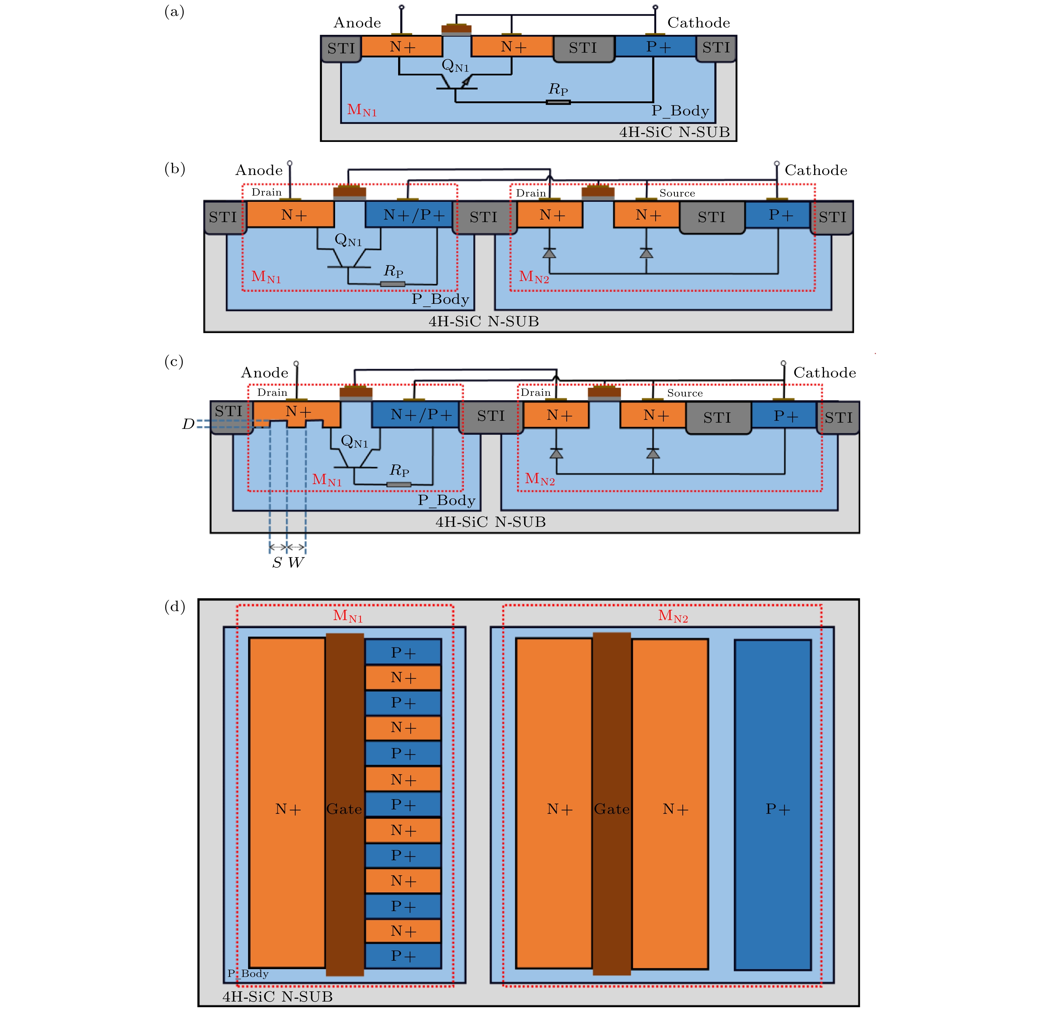
图 1 本文中所涉及到的4H-SiC ESD防护器件结构 (a) 4H-SiC GGNMOS (grounded-gate NMOS)结构; (b) 4H-SiC HHFGNMOS (high holding voltage floating gate NMOSFET)结构; (c) comb-like 4H-SiC HHFGNMOS结构; (d) comb-like 4H-SiC HHFGNMOS俯视图
Figure 1. 4H-SiC ESD protection device structure involved in this paper: (a) 4H-SiC GGNMOS (grounded gate NMOS) structure; (b) 4H-SiC HHFGNMOS (high holding voltage floating gate nMOSFET) structure; (c) comb-like 4H-SiC HHFGNMOS structure; (d) comb-like 4H-SiC HHFGNMOS top view.
图 3 4H-SiC HHFGNMOS和comb-like 4H-SiC HHFGNMOS漏区电流密度分布 (a) 4H-SiC HHFGNMOS漏区电流密度分布; (b) comb-like 4H-SiC HHFGNMOS漏区电流密度分布(W = 1 μm, S = 1 μm, D = 0.1 μm); (c) 电流密度梯度图
Figure 3. Drain current density distribution of 4H-SiC HHFGNMOS and comb-like 4H-SiC HHFGNMOS: (a) Drain current density distribution of 4H-SiC HHFGNMOS; (b) drain current density distribution of comb-like 4H-SiC HHFGNMOS (W = 1 μm, S = 1 μm, D = 0.1 μm).
图 5 Comb-like 4H-SiC HFGNMOS结构不同设计变量时漏区电流密度分布 (a) W = 1 μm, S = 1 μm, D = 0.05 μm; (b) W = 1 μm, S = 1 μm, D = 0.15 μm; (c) W = 1 μm, S = 0.5 μm, D = 0.1 μm; (d) W = 1 μm, S = 2 μm, D = 0.1 μm; (e) W = 0.5 μm, S = 1 μm, D = 0.1 μm; (f) W = 2 μm, S = 1 μm, D = 0.1 μm
Figure 5. Drain current density distribution of Comb-like 4H-SiC HHFGNMOS structure under different design variables: (a) W = 1 μm, S = 1 μm, D = 0.05 μm; (b) W = 1 μm, S = 1 μm, D = 0.15 μm; (c) W = 1 μm, S = 0.5 μm, D = 0.1 μm; (d) W = 1 μm, S = 2 μm, D = 0.1 μm; (e) W = 0.5 μm, S = 1 μm, D = 0.1 μm; (f) W = 2 μm, S = 1 μm, D = 0.1 μm.
表 1 comb-like 4H-SiC HHFGNMOS结构参数
Table 1. structural parameters of comb-like 4H-SiC HHFGNMOS.
Layer Junction depth/μm Doping concentration/cm-3 N+Implant 0.2 2.5 × 10¹⁹ P+Implant 0.2 2 × 10¹⁹ P_Body 0.7 5 × 10¹⁸ N_Epi 13 5 × 10¹⁵ -
[1] Ameraskera A, Duvvury C 2002 ESD in silicon integrated circuits (2nd Ed.) (New York: John Wiley & Sons) pp56–341
[2] Wei J, Liu S, Zhang X, Sun W, Huang A Q 2020 IEEE Trans. Power Electron 35 11299
 Google Scholar
[3] Do K I, Won J I, Koo Y S 2020 IEEE Trans. Power Electron 36 4921
 Google Scholar
[4] Do K I, Lee B S, Koo Y S 2018 IEEE Electron Device Lett 40 283
 Google Scholar
[5] Duvvury C, Diaz C H 1992 Reliability Physics Symposium 1992 30th Annual Proceedings., International San Diego, CA, USA, March 31–April 2, 1992 141
[6] Ker M D, Chen T Y 2003 IEEE Trans. Electron. Dev. 50 1050
 Google Scholar
[7] Won J I, Jung J W, Yang I S, Koo Y S 2011 Electron. Lett. 47 1072
 Google Scholar
[8] Lin H S, Shi L C 2002 Chin. J. Electron. 25 209
[9] Wang A Z H 2002 On-Chip ESD Protection for Integrated Circuits: An IC Design Perspective (Kluwer Academic Publishers) pp24–26
Catalog
Metrics
- Abstract views: 6374
- PDF Downloads: 82
- Cited By: 0


 DownLoad:


