


-
In this paper, the failure mode and mechanism of silicon carbide (SiC) Schottky barrier diode (SBD) irradiated by high-energy tantalum (Ta) ions are studied. The experimental results show that the reverse bias voltage during irradiation is the key factor causing the failure of SiC SBDs. When the reverse bias of the device is 400 V, the heavy ions will cause the single event burnout (SEB), and a “hole” formed by the melting of SiC material appears in the irradiated device. When the reverse bias is 250–300 V, the failure is manifested as the off state leakage current increases with the ion fluence. The higher the bias voltage of the device, the higher the leakage increase rate caused by heavy ions. For the devices with increased leakage, the leakage channels caused by heavy ions are found in the whole active region, based on microscopic analysis. The TCAD simulation results show that the incidence of heavy ions will lead the lattice temperature to increase in the device, and the maximum lattice temperature increases with bias voltage increasing. When the bias voltage is large enough, the local lattice temperature inside the device reaches the melting point of SiC material, resulting in SEB. When the bias voltage is relatively low, the lattice temperature is lower than the melting point of SiC material, so it will not cause burnout. However, the maximum lattice temperature in the device is concentrated near the Schottky junction, and the melting point of Schottky metal is much lower than that of SiC material. This may lead the Schottky junction to damage locally and eventually produce leakage path.
-
Keywords:
- SiC power device /
- Schottky barrier diode /
- heavy ion radiation effect
[1] Casady J B, Johnson R W 1996 Solid-State Electron. 39 1409
 Google Scholar
[2] Kimoto T, Cooper J A 2014 Fundamentals of Silicon Carbide Technology: Growth, Characterization, Devices and Applications (Singapore: John Wiley & Sons Press) p16
[3] 张林, 肖剑, 邱彦章, 程鸿亮 2011 60 056106
Google Scholar
Zhang L, Xiao J, Qiu Y Z, Cheng H L 2011 Acta Phys. Sin. 60 056106
Google Scholar
[4] Ino K, Miura M, Nakano Y, Aketa M, Kawamoto N 2019 IEEE International Conference on Electron Devices and Solid-State Circuits (EDSSC) Xi'an, China, June 12–14 2019 p1
[5] 张鸿, 郭红霞, 潘霄宇, 雷志锋, 张凤祁, 顾朝桥, 柳奕天, 琚安安, 欧阳晓平 2021 70 162401
Google Scholar
Zhang H, Guo H X, Pan X Y, Lei Z F, Zhang F Q, Gu Z Q, Liu Y T, Ju A A, Ouyang X P 2021 Acta Phys. Sin. 70 162401
Google Scholar
[6] Yu C H, Wang Y, Bao M T, Li X J, Yang J Q, Tang Z H 2021 IEEE Trans. Electron. Dev. 68 5034
Google Scholar
[7] Yu C H, Wang Y, Li X J, Liu C M, Luo X, Cao F 2018 IEEE Trans. Electron. Dev. 65 5434
Google Scholar
[8] McPherson J A, Kowal P J, Pandey G K, Chow T P, Ji W, Woodworth A A 2019 IEEE Trans. Nucl. Sci. 66 474
Google Scholar
[9] Ball D R, Hutson J M, Javanainen A, Lauenstein J M, Galloway K F, Johnson R A, Alles M L, Sternberg A L, Sierawski B D, Witulski A F, Reed R A, Schrimpf R D 2020 IEEE Trans. Nucl. Sci. 67 22
Google Scholar
[10] Akturk A, McGarrity J M, Goldsman N, Lichtenwalner D, Hull B, Grider D, Wilkins R 2018 IEEE Trans. Nucl. Sci. 65 1248
Google Scholar
[11] Witulski A F, Ball D R, Galloway K F, Javanainen A, Lauenstein J M, Sternberg A L, Schrimpf R D 2018 IEEE Trans. Nucl. Sci. 65 1951
Google Scholar
[12] Zhou X, Jia Y, Hu D, Wu Y 2019 IEEE Trans. Electron. Dev. 66 2551
Google Scholar
[13] Soelkner G, Kaindl W, Treu M, Peters D 2007 Mater. Sci. Forum 556 851
Google Scholar
[14] Martinella C, Natzke P, Alia R G, Kadi Y, Niskanen K, Rossi M, Jaatinen J, Kettunen H, Tsibizov A, Grossner U, Javanainen A 2022 Microelectron. Rel. 128 114423
Google Scholar
[15] Martinella C, Ziemann T, Stark R, Tsibizov A, Voss K O, Alia R G, Kadi Y, Grossner U, Javanainen A 2020 IEEE Trans. Nucl. Sci. 67 1381
Google Scholar
[16] Javanainen A, Galloway K F, Nicklaw C, Bosser A L, Ferlet-Cavrois V, Lauenstein J M, Pintacuda F, Reed R A, Schrimpf R D, Weller R A, Virtanen A 2017 IEEE Trans. Nucl. Sci. 64 415
Google Scholar
[17] Mizuta E, Kuboyama S, Abe H, Iwata Y, Tamura T 2014 IEEE Trans. Nucl. Sci. 61 1924
Google Scholar
[18] Javanainen A, Muinos H V, Nordlund K, Djurabekova F, Galloway K F, Turowski M, Schrimpf R D 2018 IEEE Trans. Device Mater. Reliab. 18 481
Google Scholar
[19] 于庆奎, 张洪伟, 孙毅, 梅博, 魏志超, 李晓亮, 王贺, 吕贺, 李鹏伟, 曹爽, 唐民 2019 现代应用物理 10 010602
Google Scholar
Yu Q K, Zhang H W, Sun Y, Mei B, Wei Z C, Li X L, Wang H, Li P W, Cao S, Tang M 2019 Modern Appl. Phys. 10 010602
Google Scholar
[20] Ziegler J F, Ziegler M D, Biersack J P 2010 Nucl. Instrum. Meth. Phys. Res. B 268 1818
Google Scholar
[21] Synopsys 2014 Sentaurus Device User Guide (Mountain View, CA: Synopsys Inc.) p53
[22] Shoji T, Nishida S, Hamada K, Tadano H 2014 Jap. J. Appl. Phys. 53 04EP03
Google Scholar
-
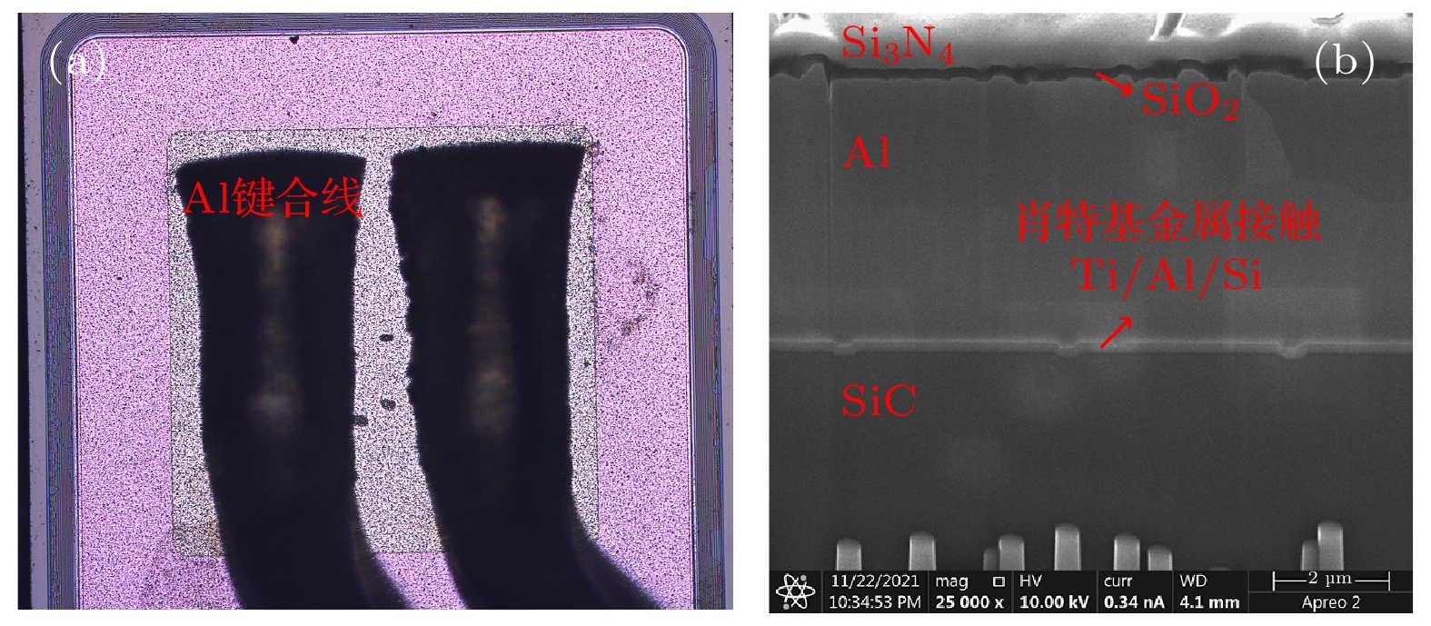
图 1 实验用SiC-SBD器件 (a) 开封后的光学显微镜顶视图; (b) 截面SEM图
Figure 1. Device of SiC-SBD used in our experiment: (a) Top view of optical microscope after de-capsulated; (b) SEM diagram of cross-section.
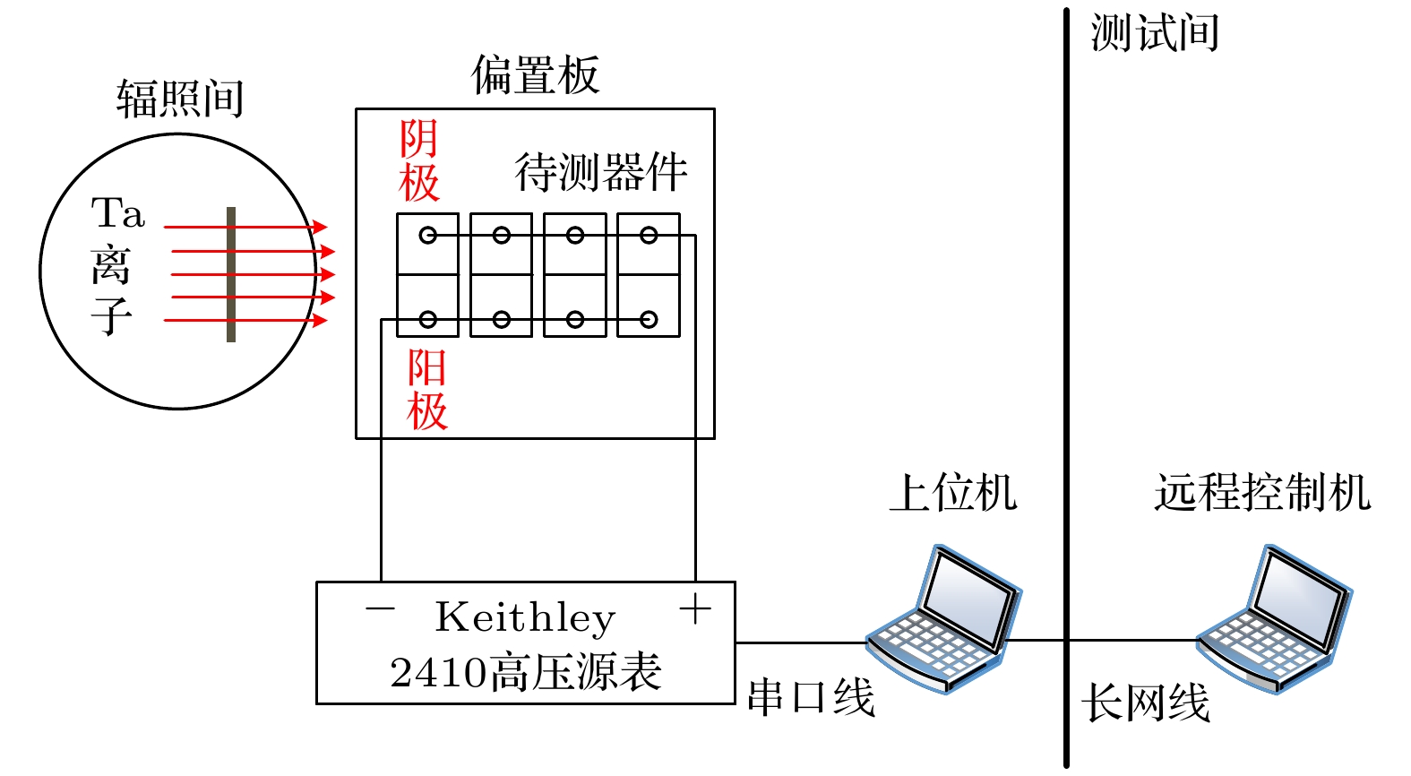
图 2 重离子辐照在线测试布局
Figure 2. On-line test layout of heavy ion irradiation.

图 3 不同偏置电压Vbias辐照过程中, 器件关态漏电流随时间的变化关系 (a) Vbias = 100—300 V; (b) Vbias = 400 V
Figure 3. Off-state leakage current as a function of time during irradiation under different biases Vbias: (a) Vbias= 100–300 V; (b) Vbias = 400 V.

图 4 辐照后器件的EMMI测试结果 (a) SEB的器件; (b)关态漏电增加的器件
Figure 4. EMMI analysis results for the irradiated devices: (a) Device of SEB; (b) device with leakage current increase.

图 5 发生SEB的SBD器件的失效区域SEM图像 (a) 顶视图; (b)—(f) 分别对应位置1—5处的截面图
Figure 5. SEM images of failure area for SBD device with SEB: (a) Top view; (b)–(f) cross-section image corresponding to the line 1–5, respectively.
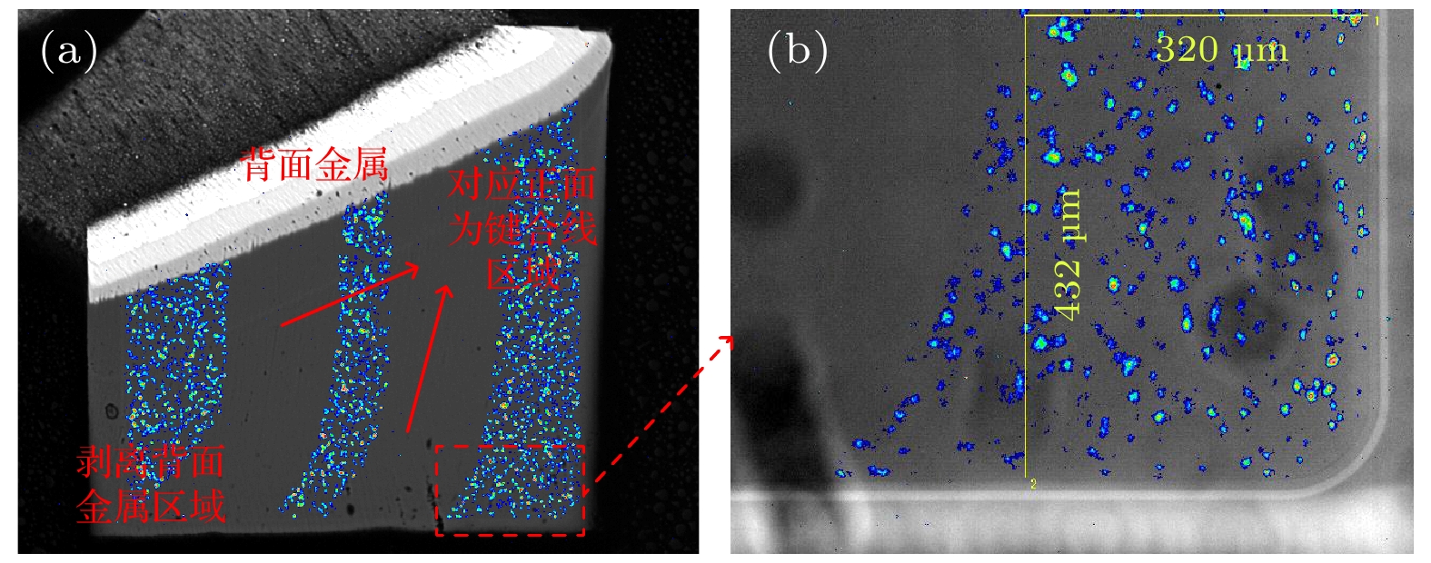
图 6 (a) 关态漏电增加器件背面的EMMI测试结果; (b) 320 μm×432 μm区域的局部放大图(图(a)红色虚线范围)
Figure 6. (a) Back-side EMMI analysis result for the irradiated device with leakage current increase; (b) enlarged view of 320 μm×432 μm area (Area surrounded by the red dotted line in Fig.(a)).

图 7 器件截面SEM形貌图 (a) 辐照后发生漏电增加的器件; (b) 未辐照器件
Figure 7. SEM morphology of the device cross-section: (a) The irradiated device of leakage current increasing; (b) pristine device.
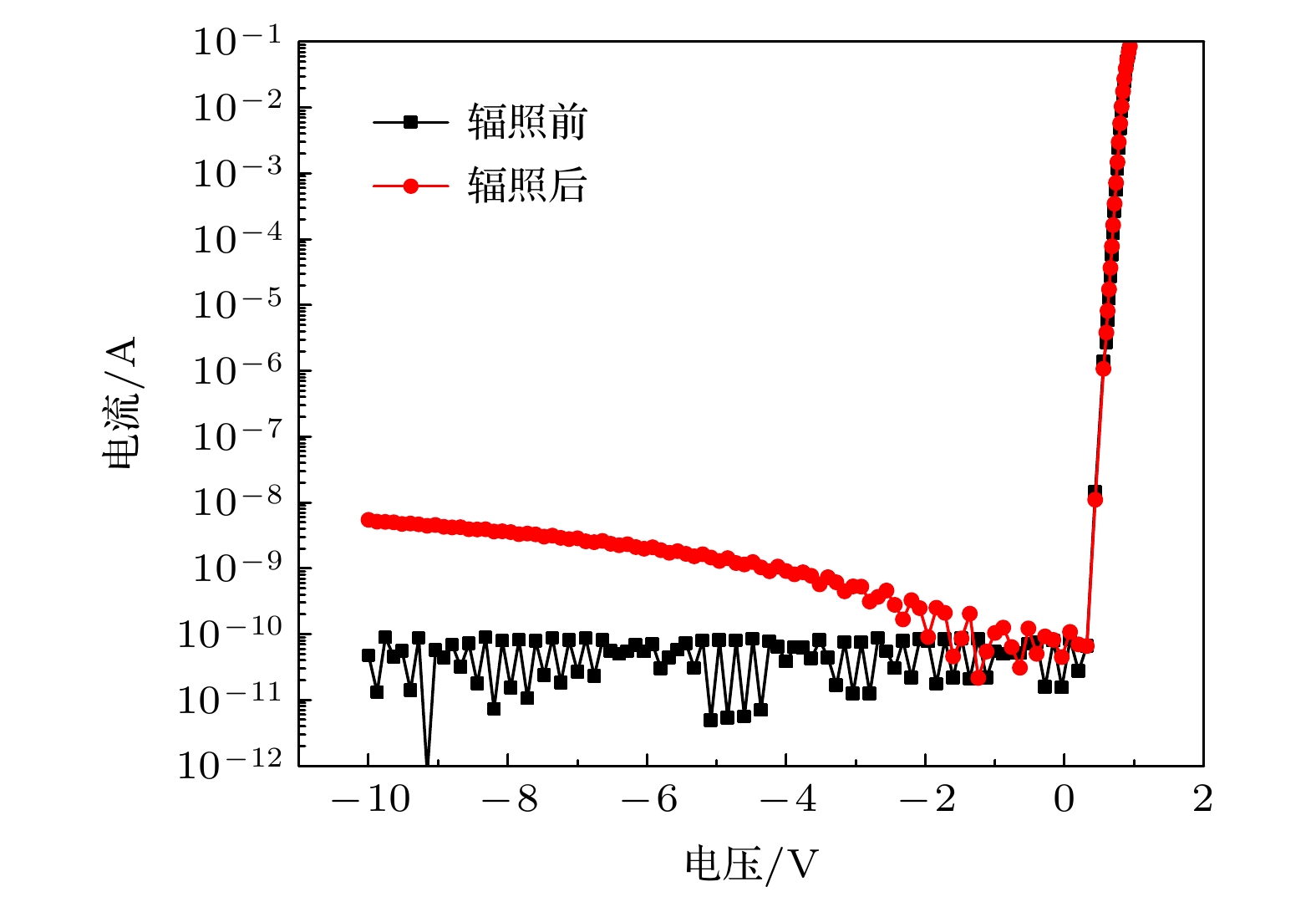
图 8 发生漏电增加器件辐照前后的I-V特性曲线
Figure 8. I-V characteristics of the device with the leakage current increase before and after irradiation.
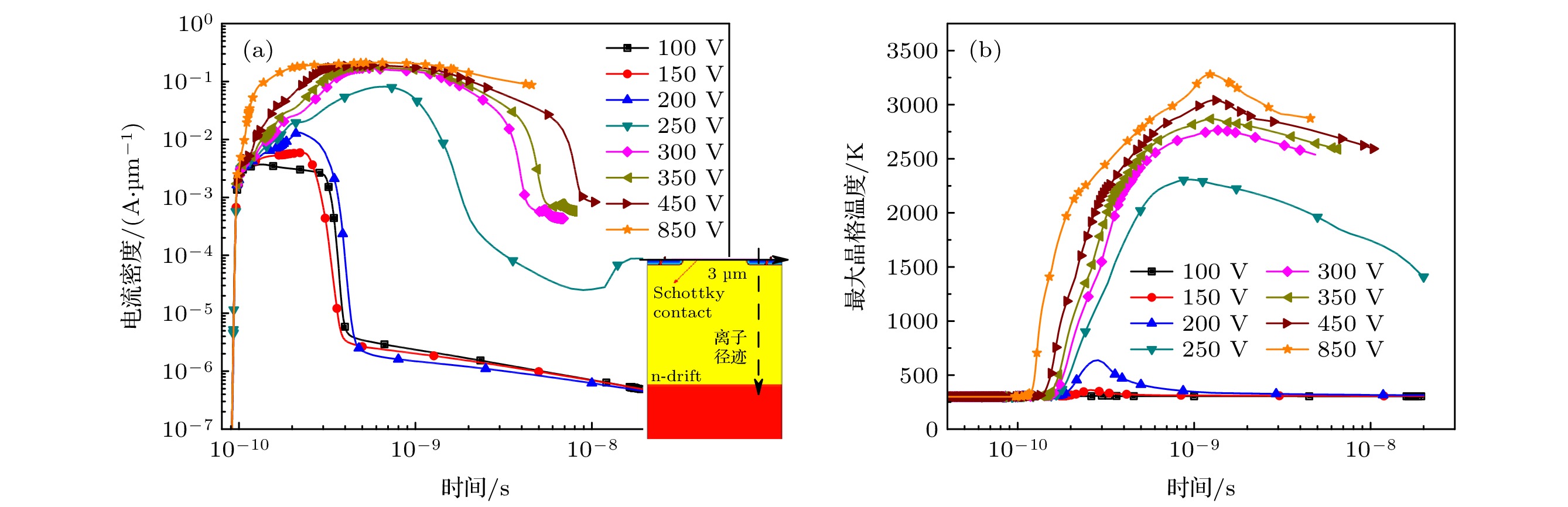
图 9 不同反向偏压下离子入射导致的(a)阴极瞬态电流密度和(b)最大晶格温度随时间的变化
Figure 9. (a) Transient current density and (b) maximum lattice temperature as a function of time when heavy ion strikes under the different bias voltages.

图 10 离子入射SBD导致的沿离子径迹上的电场分布仿真 (a) Vr = 850 V; (b) Vr = 250 V
Figure 10. Simulated electric field as a function of distance along the ion track: (a) Vr = 850 V; (b) Vr = 250 V.

图 11 重离子入射不同时间后SiC-SBD器件内部的晶格温度分布 (a) 400 ps; (b) 1 ns; (c) 5 ns; (d) 10 ns
Figure 11. Simulation of lattice temperature in SiC-SBD after the heavy ion incidence at different times: (a) 400 ps; (b) 1 ns; (c) 5 ns; (d) 10 ns.
-
[1] Casady J B, Johnson R W 1996 Solid-State Electron. 39 1409
Google Scholar
[2] Kimoto T, Cooper J A 2014 Fundamentals of Silicon Carbide Technology: Growth, Characterization, Devices and Applications (Singapore: John Wiley & Sons Press) p16
[3] 张林, 肖剑, 邱彦章, 程鸿亮 2011 60 056106
Google Scholar
Zhang L, Xiao J, Qiu Y Z, Cheng H L 2011 Acta Phys. Sin. 60 056106
Google Scholar
[4] Ino K, Miura M, Nakano Y, Aketa M, Kawamoto N 2019 IEEE International Conference on Electron Devices and Solid-State Circuits (EDSSC) Xi'an, China, June 12–14 2019 p1
[5] 张鸿, 郭红霞, 潘霄宇, 雷志锋, 张凤祁, 顾朝桥, 柳奕天, 琚安安, 欧阳晓平 2021 70 162401
Google Scholar
Zhang H, Guo H X, Pan X Y, Lei Z F, Zhang F Q, Gu Z Q, Liu Y T, Ju A A, Ouyang X P 2021 Acta Phys. Sin. 70 162401
Google Scholar
[6] Yu C H, Wang Y, Bao M T, Li X J, Yang J Q, Tang Z H 2021 IEEE Trans. Electron. Dev. 68 5034
Google Scholar
[7] Yu C H, Wang Y, Li X J, Liu C M, Luo X, Cao F 2018 IEEE Trans. Electron. Dev. 65 5434
Google Scholar
[8] McPherson J A, Kowal P J, Pandey G K, Chow T P, Ji W, Woodworth A A 2019 IEEE Trans. Nucl. Sci. 66 474
Google Scholar
[9] Ball D R, Hutson J M, Javanainen A, Lauenstein J M, Galloway K F, Johnson R A, Alles M L, Sternberg A L, Sierawski B D, Witulski A F, Reed R A, Schrimpf R D 2020 IEEE Trans. Nucl. Sci. 67 22
Google Scholar
[10] Akturk A, McGarrity J M, Goldsman N, Lichtenwalner D, Hull B, Grider D, Wilkins R 2018 IEEE Trans. Nucl. Sci. 65 1248
Google Scholar
[11] Witulski A F, Ball D R, Galloway K F, Javanainen A, Lauenstein J M, Sternberg A L, Schrimpf R D 2018 IEEE Trans. Nucl. Sci. 65 1951
Google Scholar
[12] Zhou X, Jia Y, Hu D, Wu Y 2019 IEEE Trans. Electron. Dev. 66 2551
Google Scholar
[13] Soelkner G, Kaindl W, Treu M, Peters D 2007 Mater. Sci. Forum 556 851
Google Scholar
[14] Martinella C, Natzke P, Alia R G, Kadi Y, Niskanen K, Rossi M, Jaatinen J, Kettunen H, Tsibizov A, Grossner U, Javanainen A 2022 Microelectron. Rel. 128 114423
Google Scholar
[15] Martinella C, Ziemann T, Stark R, Tsibizov A, Voss K O, Alia R G, Kadi Y, Grossner U, Javanainen A 2020 IEEE Trans. Nucl. Sci. 67 1381
Google Scholar
[16] Javanainen A, Galloway K F, Nicklaw C, Bosser A L, Ferlet-Cavrois V, Lauenstein J M, Pintacuda F, Reed R A, Schrimpf R D, Weller R A, Virtanen A 2017 IEEE Trans. Nucl. Sci. 64 415
Google Scholar
[17] Mizuta E, Kuboyama S, Abe H, Iwata Y, Tamura T 2014 IEEE Trans. Nucl. Sci. 61 1924
Google Scholar
[18] Javanainen A, Muinos H V, Nordlund K, Djurabekova F, Galloway K F, Turowski M, Schrimpf R D 2018 IEEE Trans. Device Mater. Reliab. 18 481
Google Scholar
[19] 于庆奎, 张洪伟, 孙毅, 梅博, 魏志超, 李晓亮, 王贺, 吕贺, 李鹏伟, 曹爽, 唐民 2019 现代应用物理 10 010602
Google Scholar
Yu Q K, Zhang H W, Sun Y, Mei B, Wei Z C, Li X L, Wang H, Li P W, Cao S, Tang M 2019 Modern Appl. Phys. 10 010602
Google Scholar
[20] Ziegler J F, Ziegler M D, Biersack J P 2010 Nucl. Instrum. Meth. Phys. Res. B 268 1818
Google Scholar
[21] Synopsys 2014 Sentaurus Device User Guide (Mountain View, CA: Synopsys Inc.) p53
[22] Shoji T, Nishida S, Hamada K, Tadano H 2014 Jap. J. Appl. Phys. 53 04EP03
Google Scholar


 DownLoad:


Catalog
Metrics
- Abstract views: 9437
- PDF Downloads: 165
- Cited By: 0
