


-
In an electronic double-layer system composed of two spatially adjacent but electrically insulated conductors, when current flows through one conductor (drive layer), its charge carriers transfer energy/momentum to the charge carriers in the other conductor (drag layer) through interlayer Coulomb coupling, thus generating a measurable voltage or current in the drag layer. This phenomenon is known as the interlayer drag effect. This effect provides a critical approach for studying quasiparticle interactions and investigating interlayer-correlated quantum states. Two-dimensional layered materials with highly tunable properties provide new opportunities for exploring the drag effect. In this study, we fabricate an electronic double-layer structure consisting of graphene and NbSe2 to systematically investigate the drag effect between a two-dimensional semimetal and a two-dimensional superconductor, wherein a thin hBN layer serves as the insulating spacer. When graphene acts as the drive layer and NbSe2 acts as the drag layer, a significant positive drag response is observed within the superconducting transition temperature range of NbSe2. In contrast, the drag signal vanishes when NbSe2 is in its normal metallic state. The measurements of magnetic field dependence reveal that the drag response disappears under high fields where the superconductivity of NbSe2 is suppressed, further confirming its direct correlation with the superconducting transition. The gate-voltage modulation experiments reveal that the drag response peaks when adjusting the Fermi level of graphene across the Dirac point. This is attributed to the reduced screening of interlayer interactions due to the ultra-low carrier concentration at this point. Notably, the sign of the supercurrent drag does not depend on the carrier type in graphene, ruling out the traditional momentum-transfer drag mechanism. Our results collectively demonstrate the realization of supercurrent drag effect, which has been attributed to Coulomb coupling between the quantum fluctuations of the superconducting phases in a superconductor and the charge densities in a normal conductor in previous study. Notably, by comparing different devices, it is found that this type of supercurrent drag responses occurs only in the thin NbSe2 layers cleaved in air. No significant signals are detected in thick NbSe2 layers or thin layers cleaved under the protection of argon. These results establish the importance of superconducting inhomogeneity in NbSe2 for generating supercurrent drag effect, indicating that drag measurements can also serve as a novel probe for investigating superconducting properties. Further investigation into the polarity and intensity of supercurrent drag signals may advance our understanding of inhomogeneous superconductivity, as well as interactions between normal carriers and Cooper pairs.
-
Keywords:
- two-dimensional materials /
- supercurrent drag effect /
- superconducting inhomogeneity /
- quantum fluctuations
[1] Narozhny B N, Levchenko A 2016 Rev. Mod. Phys. 88 025003
 Google Scholar
[2] Laroche D, Gervais G, Lilly M P, Reno J L 2014 Science 343 631
Google Scholar
[3] Yamamoto M, Stopa M, Tokura Y, Hirayama Y, Tarucha S 2006 Science 313 204
Google Scholar
[4] Eisenstein J P, MacDonald A H 2004 Nature 432 691
Google Scholar
[5] Tutuc E, Shayegan M, Huse D A 2004 Phys. Rev. Lett. 93 036802
Google Scholar
[6] Su J J, MacDonald A H 2008 Nat. Phys. 4 799
Google Scholar
[7] Liu X, Watanabe K, Taniguchi T, Halperin B I, Kim P 2017 Nat. Phys. 13 746
Google Scholar
[8] Li J I A, Taniguchi T, Watanabe K, Hone J, Dean C R 2017 Nat. Phys. 13 751
Google Scholar
[9] Giaever I 1966 Phys. Rev. Lett. 16 460
Google Scholar
[10] Duan J M, Yip S 1993 Phys. Rev. Lett. 70 3647
Google Scholar
[11] Shimshoni E 1995 Phys. Rev. B 51 9415
Google Scholar
[12] Huang X, Bazàn G, Bernstein G H 1995 Phys. Rev. Lett. 74 4051
Google Scholar
[13] Giordano N, Monnier J D 1994 Phys. Rev. B 50 9363
Google Scholar
[14] Kim S, Jo I, Nah J, Yao Z, Banerjee S K, Tutuc E 2011 Phys. Rev. B 83 161401
Google Scholar
[15] Gorbachev R V, Geim A K, Katsnelson M I, Novoselov K S, Tudorovskiy T, Grigorieva I V, MacDonald A H, Morozov S V, Watanabe K, Taniguchi T, Ponomarenko L A 2012 Nat. Phys. 8 896
Google Scholar
[16] Tao R, Li L, Xie H Y, Fan X D, Guo L H, Zhu L J, Yan Y D, Zhang Z Y, Zeng C G 2023 Nat. Phys. 19 372
Google Scholar
[17] Xi X X, Wang Z F, Zhao W W, Park J H, Law K T, Berger H, Forró L, Shan J, Mak K F 2016 Nat. Phys. 12 139
Google Scholar
[18] Khestanova E, Birkbeck J, Zhu M, Cao Y, Yu G L, Ghazaryan D, Yin J, Berger H, Forró L, Taniguchi T, Watanabe K, Gorbachev R V, Mishchenko A, Geim A K, Grigorieva I V 2018 Nano Lett. 18 2623
Google Scholar
[19] Onishi S, Ugeda M M, Zhang Y, Chen Y, Ojeda-Aristizabal C, Ryu H, Mo S K, Hussain Z, Shen Z X, Crommie M F, Zettl A 2016 Phys. Status Solidi B 253 2396
Google Scholar
[20] El-Bana M S, Wolverson D, Russo S, Balakrishnan G, Paul D M, Bending S J 2013 Supercond. Sci. Technol. 26 125020
Google Scholar
[21] Cao Y, Mishchenko A, Yu G L, Khestanova E, Rooney A P, Prestat E, Kretinin A V, Blake P, Shalom M B, Woods C, Chapman J, Balakrishnan G, Grigorieva I V, Novoselov K S, Piot B A, Potemski M, Watanabe K, Taniguchi T, Haigh S J, Geim A K, Gorbachev R V 2015 Nano Lett. 15 4914
Google Scholar
[22] Myers G E, Montet G L 1971 J. Phys. Chem. Solids 32 2645
Google Scholar
[23] Chen Z, Swartz A G, Yoon H, Inoue H, Merz T A, Lu D, Xie Y, Yuan H, Hikita Y, Raghu S, Hwang H Y 2018 Nat. Commun. 9 4008
Google Scholar
[24] Bert J A, Kalisky B, Bell C, Kim M, Hikita Y, Hwang H Y, Moler K A 2011 Nat. Phys. 7 767
Google Scholar
-
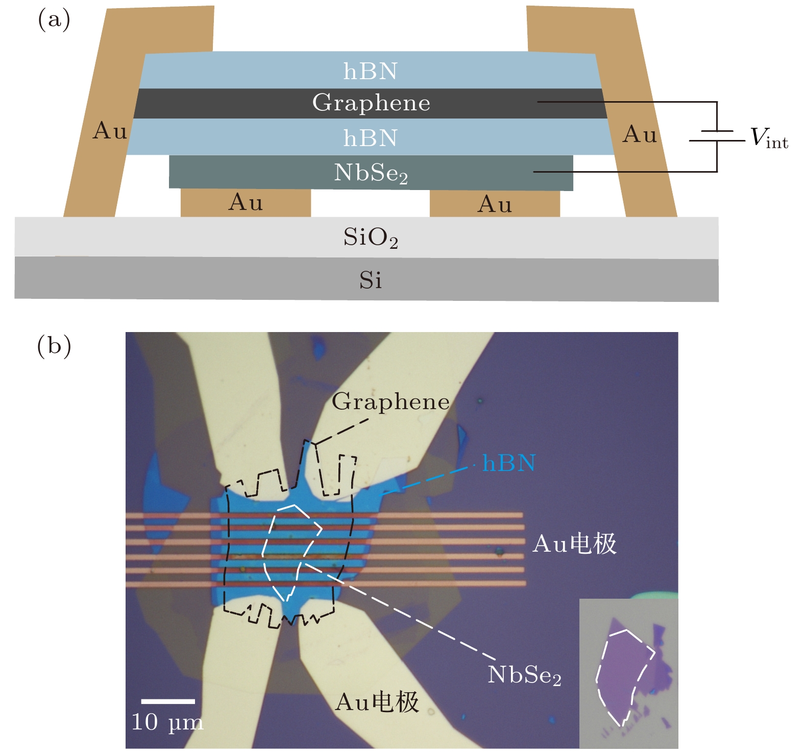
图 1 (a)石墨烯-NbSe2拖拽器件示意图; (b)石墨烯-NbSe2拖拽器件的光学显微图像, 单层石墨烯和双层NbSe2的轮廓分别用黑白虚线标示, 插图为转移前NbSe2层的光学显微图像
Figure 1. (a) Schematic diagram of graphene-NbSe2 drag device; (b) optical image of graphene-NbSe2 drag device, the outlines of monolayer graphene and NbSe2 flakes are marked with black and white dashed lines, respectively. Inset is the optical image of the NbSe2 layer before transfer.
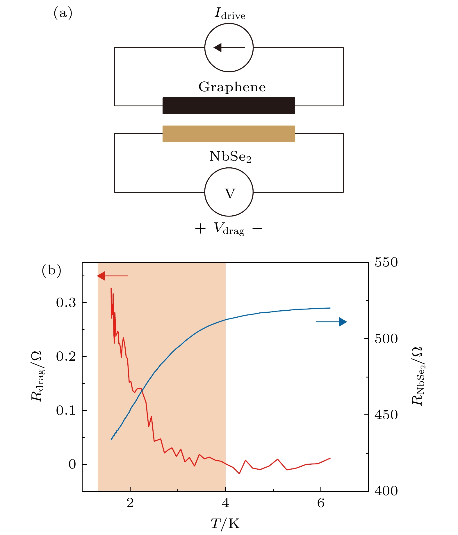
图 2 (a)拖拽测试示意图; (b)器件#1中层间拖拽电阻(Rdrag)和NbSe2层内电阻($ {{R}}_{{\text{NbSe}}_{2}} $)随温度的变化曲线
Figure 2. (a) Schematic of the setup for drag measurements; (b) interlayer drag resistance (Rdrag) and intralayer resistance of NbSe2 ($ {{R}}_{{\text{NbSe}}_{2}} $) as functions of temperature for Device #1.
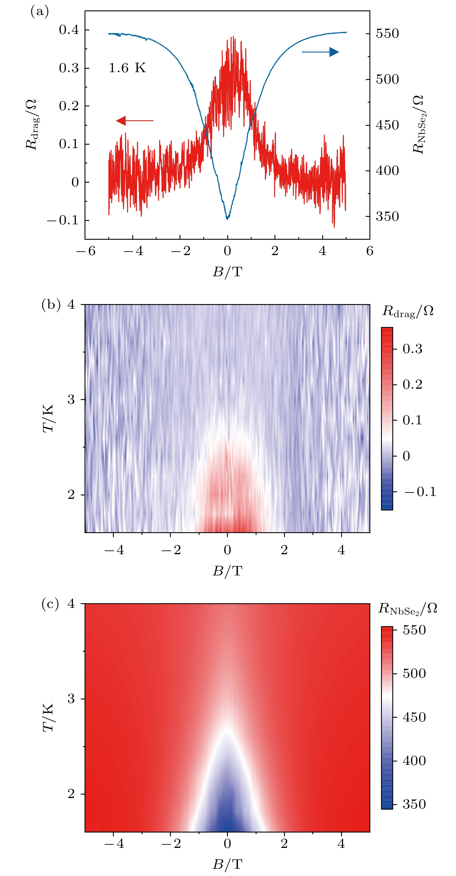
图 3 (a)器件#1中Rdrag和$ {{R}}_{{\text{NbSe}}_{2}} $随磁场强度的变化曲线, 测试温度为1.6 K; (b) Rdrag和(c) $ {{R}}_{{\text{NbSe}}_{2}} $随温度和磁场强度的变化
Figure 3. (a) Rdrag and $ {{R}}_{{\text{NbSe}}_{2}} $ as functions of magnetic field for Device #1, measured at 1.6 K; (b) Rdrag and (c) $ {{R}}_{{\text{NbSe}}_{2}} $ as functions of temperature and magnetic field.
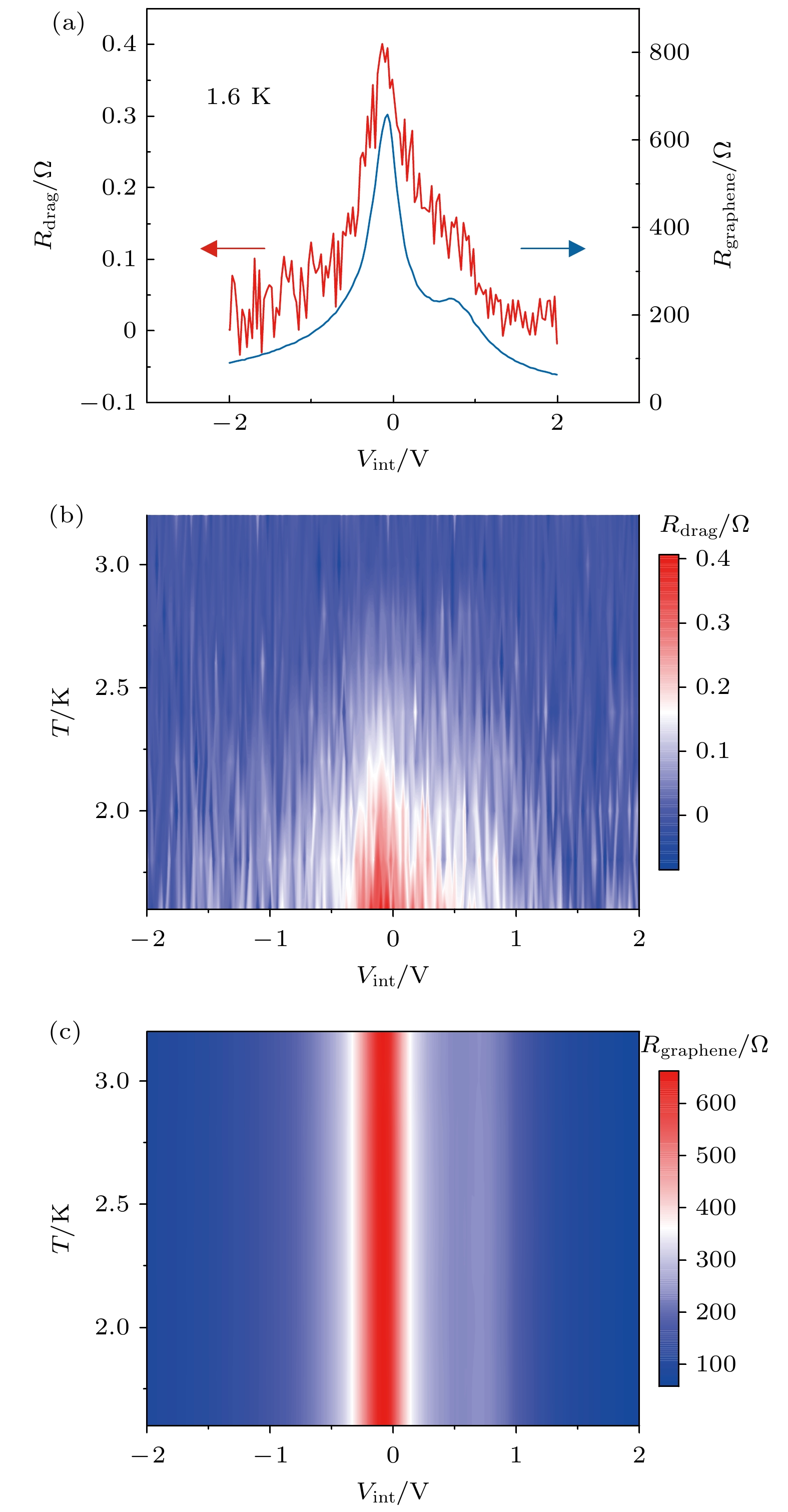
图 4 (a)器件#1中Rdrag和石墨烯层内电阻Rgraphene随层间栅压的变化曲线, 测试温度为1.6 K; (b) Rdrag和(c) Rgraphene随温度和层间栅压的变化
Figure 4. (a) Rdrag and intralayer resistance of graphene (Rgraphene) as functions of interlayer gate voltage (Vint) for Device #1, measured at 1.6 K; (b) Rdrag and (c) Rgraphene as functions of temperature and Vint.
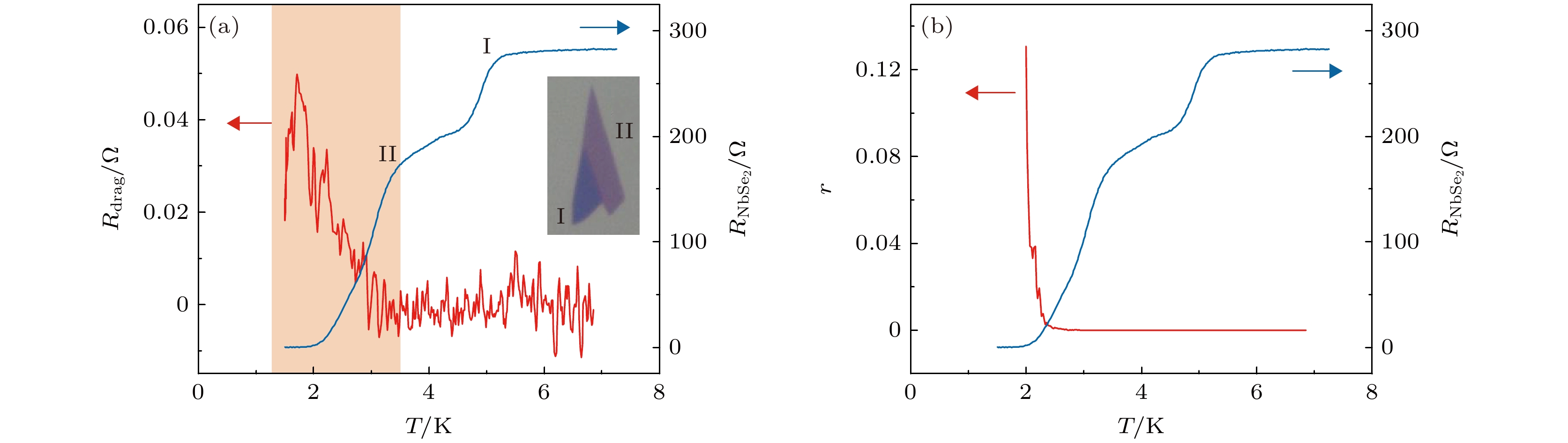
图 5 (a)器件#2中Rdrag和$ {{R}}_{{\text{NbSe}}_{2}} $随温度的变化曲线, 插图为该器件中所使用的NbSe2层的光学显微图像, 由薄层区域(~3层)和厚层区域(~5层)两部分构成; (b)拖拽耦合比r和$ {{R}}_{{\text{NbSe}}_{2}} $随温度的变化曲线
Figure 5. (a) Rdrag and $ {{R}}_{{\text{NbSe}}_{2}} $ as functions of temperature for Device #2, inset is optical image of the NbSe2 layer in this device, which is composed of a thin region I (~3 layers) and a thick region II (~5 layers); (b) passive-to-active ratio r (drag current/drive current) and $ {{R}}_{{\text{NbSe}}_{2}} $ as functions of temperature.
-
[1] Narozhny B N, Levchenko A 2016 Rev. Mod. Phys. 88 025003
Google Scholar
[2] Laroche D, Gervais G, Lilly M P, Reno J L 2014 Science 343 631
Google Scholar
[3] Yamamoto M, Stopa M, Tokura Y, Hirayama Y, Tarucha S 2006 Science 313 204
Google Scholar
[4] Eisenstein J P, MacDonald A H 2004 Nature 432 691
Google Scholar
[5] Tutuc E, Shayegan M, Huse D A 2004 Phys. Rev. Lett. 93 036802
Google Scholar
[6] Su J J, MacDonald A H 2008 Nat. Phys. 4 799
Google Scholar
[7] Liu X, Watanabe K, Taniguchi T, Halperin B I, Kim P 2017 Nat. Phys. 13 746
Google Scholar
[8] Li J I A, Taniguchi T, Watanabe K, Hone J, Dean C R 2017 Nat. Phys. 13 751
Google Scholar
[9] Giaever I 1966 Phys. Rev. Lett. 16 460
Google Scholar
[10] Duan J M, Yip S 1993 Phys. Rev. Lett. 70 3647
Google Scholar
[11] Shimshoni E 1995 Phys. Rev. B 51 9415
Google Scholar
[12] Huang X, Bazàn G, Bernstein G H 1995 Phys. Rev. Lett. 74 4051
Google Scholar
[13] Giordano N, Monnier J D 1994 Phys. Rev. B 50 9363
Google Scholar
[14] Kim S, Jo I, Nah J, Yao Z, Banerjee S K, Tutuc E 2011 Phys. Rev. B 83 161401
Google Scholar
[15] Gorbachev R V, Geim A K, Katsnelson M I, Novoselov K S, Tudorovskiy T, Grigorieva I V, MacDonald A H, Morozov S V, Watanabe K, Taniguchi T, Ponomarenko L A 2012 Nat. Phys. 8 896
Google Scholar
[16] Tao R, Li L, Xie H Y, Fan X D, Guo L H, Zhu L J, Yan Y D, Zhang Z Y, Zeng C G 2023 Nat. Phys. 19 372
Google Scholar
[17] Xi X X, Wang Z F, Zhao W W, Park J H, Law K T, Berger H, Forró L, Shan J, Mak K F 2016 Nat. Phys. 12 139
Google Scholar
[18] Khestanova E, Birkbeck J, Zhu M, Cao Y, Yu G L, Ghazaryan D, Yin J, Berger H, Forró L, Taniguchi T, Watanabe K, Gorbachev R V, Mishchenko A, Geim A K, Grigorieva I V 2018 Nano Lett. 18 2623
Google Scholar
[19] Onishi S, Ugeda M M, Zhang Y, Chen Y, Ojeda-Aristizabal C, Ryu H, Mo S K, Hussain Z, Shen Z X, Crommie M F, Zettl A 2016 Phys. Status Solidi B 253 2396
Google Scholar
[20] El-Bana M S, Wolverson D, Russo S, Balakrishnan G, Paul D M, Bending S J 2013 Supercond. Sci. Technol. 26 125020
Google Scholar
[21] Cao Y, Mishchenko A, Yu G L, Khestanova E, Rooney A P, Prestat E, Kretinin A V, Blake P, Shalom M B, Woods C, Chapman J, Balakrishnan G, Grigorieva I V, Novoselov K S, Piot B A, Potemski M, Watanabe K, Taniguchi T, Haigh S J, Geim A K, Gorbachev R V 2015 Nano Lett. 15 4914
Google Scholar
[22] Myers G E, Montet G L 1971 J. Phys. Chem. Solids 32 2645
Google Scholar
[23] Chen Z, Swartz A G, Yoon H, Inoue H, Merz T A, Lu D, Xie Y, Yuan H, Hikita Y, Raghu S, Hwang H Y 2018 Nat. Commun. 9 4008
Google Scholar
[24] Bert J A, Kalisky B, Bell C, Kim M, Hikita Y, Hwang H Y, Moler K A 2011 Nat. Phys. 7 767
Google Scholar


 DownLoad:


Catalog
Metrics
- Abstract views: 669
- PDF Downloads: 54
- Cited By: 0
