


-
With the gradual increase in size requirements for integrated circuit fabrication, the research on the miniaturization of electronic device is increasingly favored by more and more scientists. In this work, the edge modifications of the electronic band structure of α-2-graphyne and electronic transport characteristics of its devices are systematically investigated by employing the density functional theory combined with non-equilibrium Green's functions. The research results of the band structures doped with halogens or oxygenated group show that when the various elements are doped into the antiferromagnetic configuration of α-2-graphyne, the materials exhibit unique semiconductor properties. In particular, the periodic structure of α-2-graphyne with the O-doping exhibits relatively complex band structures near the Fermi level. It can be found that the electronic devices doped with F, Cl, O, OH show obvious negative differential resistance (NDR) and spin filtering effects. Among them, the NDR effect of the device with O doping (M4) shows particularly significant feature, and its peak-to-valley ratio in the antiparallel case is as high as 136. However, the peak-to-valley ratio reaches 128 in the antiferromagnetism configuration. In addition, the intrinsic physical mechanism of the NDR effect is further dissected by calculating the transmission spectra and local densities of states in the parallel case and antiparallel case. At the same time, the spin filtering efficiency of the device reaches a value as high as 84% at an applied voltage of -0.4 V in the parallel case and 79% at -1.6 V in the antiparallel case. By analyzing the electron transport paths of the M4, the intrinsic mechanism of the spin-filtering properties can be clearly understood for the devices based on the α-2-graphyne nanotibbons. This research has significant application value in the hot research t areas such as novel logic devices, integrated circuits, and micro/nano-electronic machines.
-
Keywords:
- α-2-graphyne /
- first principles /
- edge modification /
- negative differential resistance effect /
- spin filtering effect
-
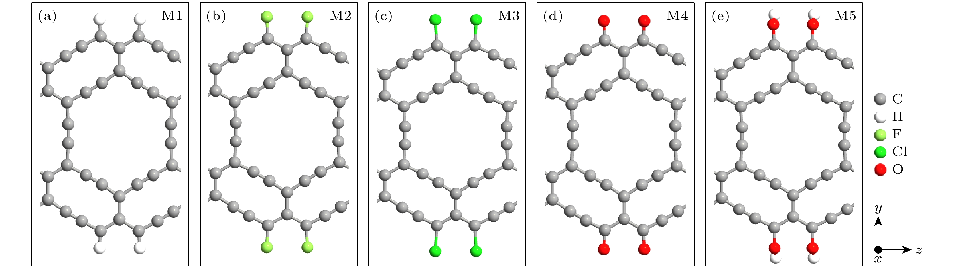
图 1 (a)—(e) M1—M5为α-2-GY边缘碳原子分别被H, F, Cl, O, OH边缘钝化的结构模型图. 右侧灰色、白色、绿色、深绿色、红色圆点分别代表C, H, F, Cl, O等元素, 坐标轴指示了周期性元胞的取向
Figure 1. (a)–(e) M1–M5 show the structural diagrams of α-2-GY with the edge carbon atoms passivated by H, F, Cl, O or OH atoms, respectively. The gray, white, green, olive and red circles on the right part represent the elements of C, H, F, Cl and O, respectively, and the coordinate axes indicate the orientation of the periodic cells.
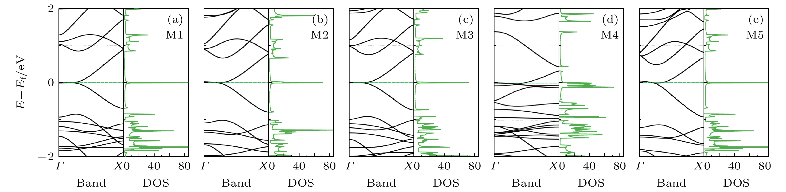
图 2 在NM下(a)—(e) M1—M5模型的能带结构图(左图)与态密度(density of states, DOS)分布图(右图). 绿色虚线代表费米能级
Figure 2. Energy band structure diagrams (left) and the distribution on the density of states (DOS) (right) for the (a)–(e) M1–M5 model within the NM state; the green dashed line represents the Fermi energy level.
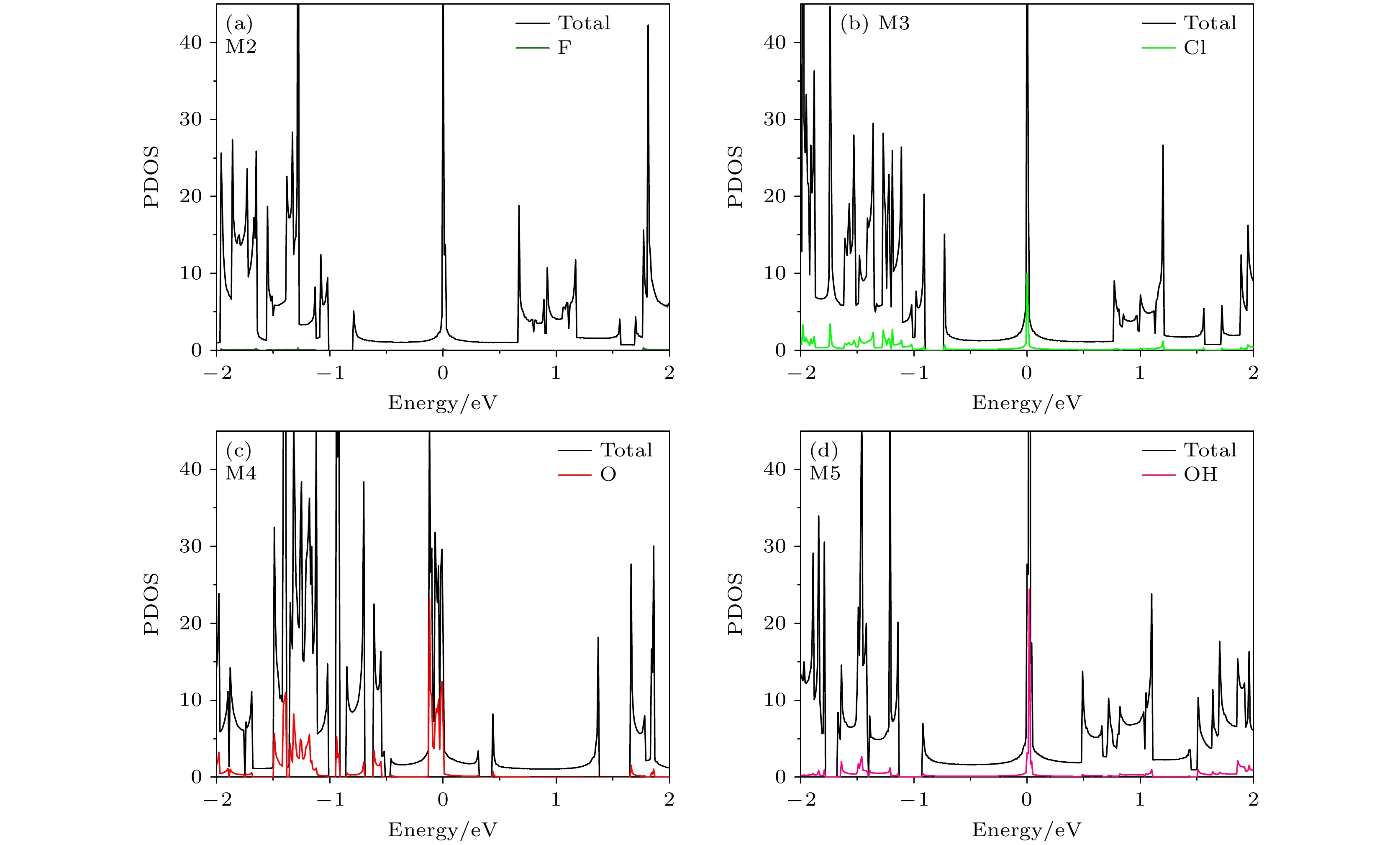
图 3 在NM态下(a)—(d) M2—M5的PDOS分布图, 能量零点设置为费米能级
Figure 3. (a)–(d) The distribution on the PDOS for the M2–M5 within the NM state, and the Fermi energy level is set to zero.
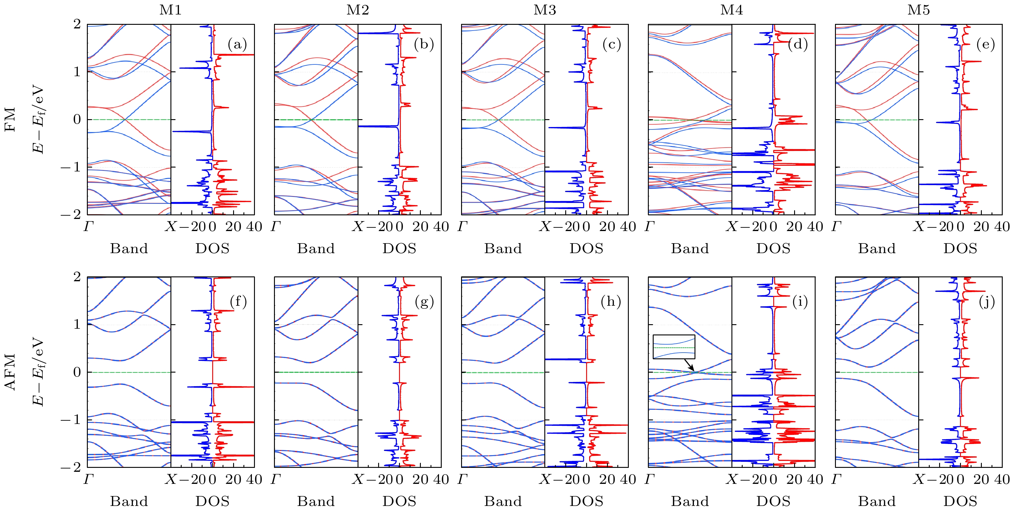
图 4 (a)—(e)/(f)—(j) M1—M5模型在FM/AFM构型态下的能带结构图和DOS分布图; 蓝色/红色实线表示自旋向上(SU)/向下(SD)的自旋方向; 绿色虚线指示对应的费米能级
Figure 4. (a)–(e)/(f)–(j) The energy band structure maps and DOS distributions of the M1–M5 models within the FM/AFM states; the blue/red solid lines indicate the spin-up (SU)/-down (SD) directions; the green dashed lines indicate the corresponding Fermi energy levels.
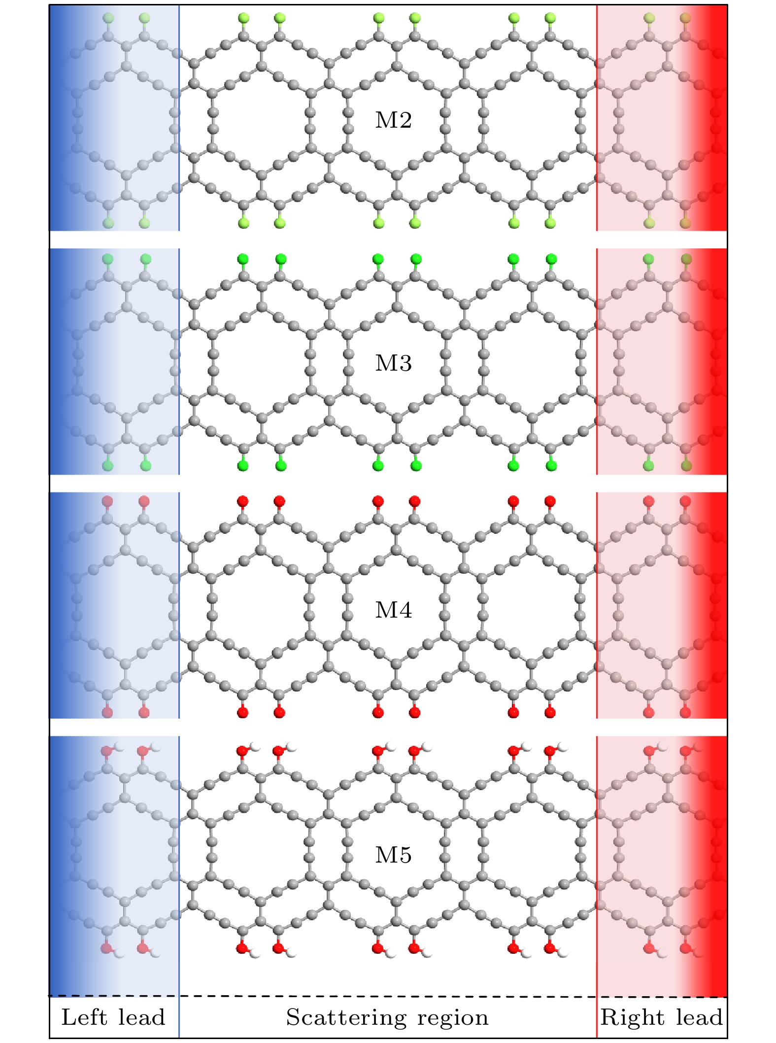
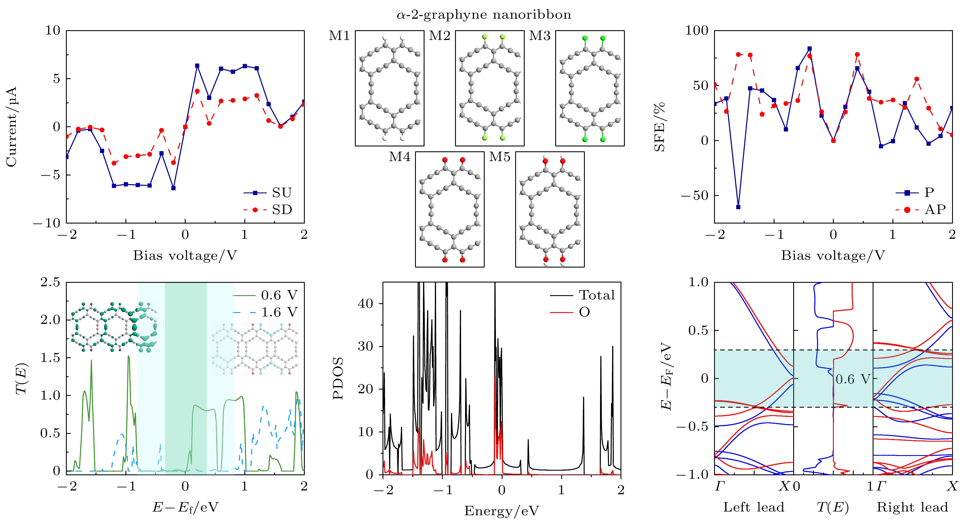
图 5 M2—M5分别是由F, Cl, O, OH边缘钝化的分子结器件模型图. 器件M2—M5左/右两端的蓝/红色渐变阴影部分分别代表器件的左/右电极, 中间部分为散射区
Figure 5. M2–M5 are model diagrams of molecular junction devices, which are passivated by F, Cl, O or OH group, respectively. The blue/red gradient shaded portions at left/right sides of M2–M5 represent the left/right leads of the device, and the middle portion is the scattering region.
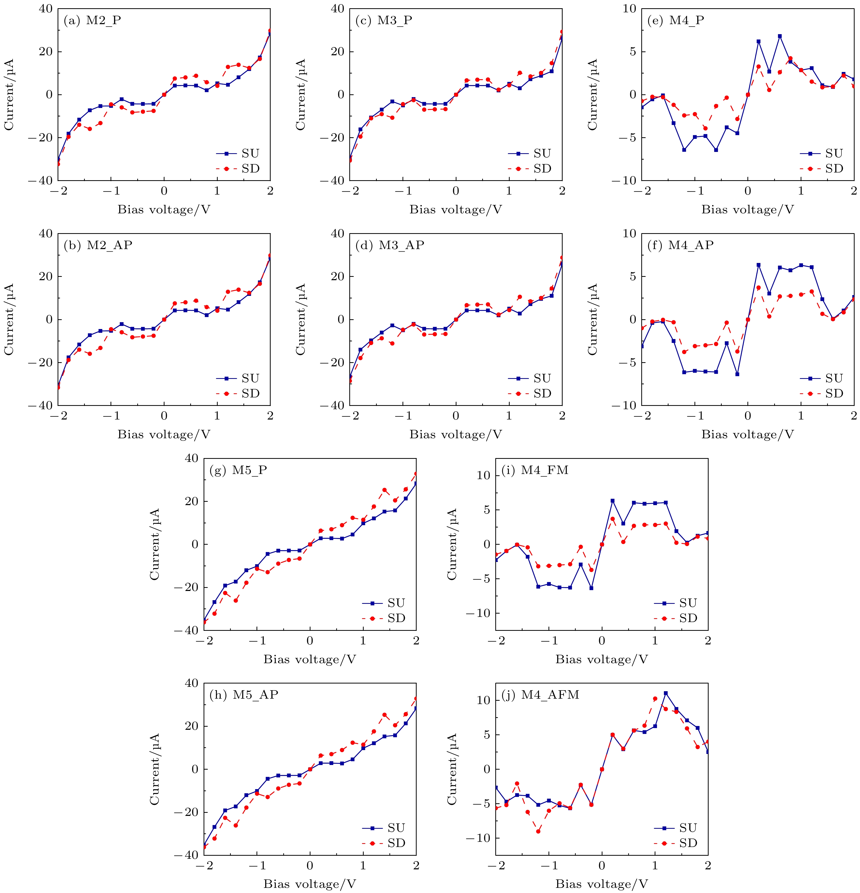
图 6 该图展示器件(a), (b) M2, (c), (d) M3, (e), (f) M4, (g), (h) M5在P和AP自旋组态下的伏安特性(current-voltage, I-V)曲线; (i), (j)器件M4在FM/AFM磁性配置下的I-V曲线; 蓝色实线/红色虚线分别表示SU/SD自旋方向的电流
Figure 6. The insets demonstrate the I-V curves of devices (a), (b) M2, (c), (d) M3, (e), (f) M4, and (g), (h) M5 within the P and AP spin grouping state; (i), (j) are the I-V curves of M4 within the FM/AFM magnetic configuration; the blue solid/red dashed lines denote the SU/SD directions, respectively.
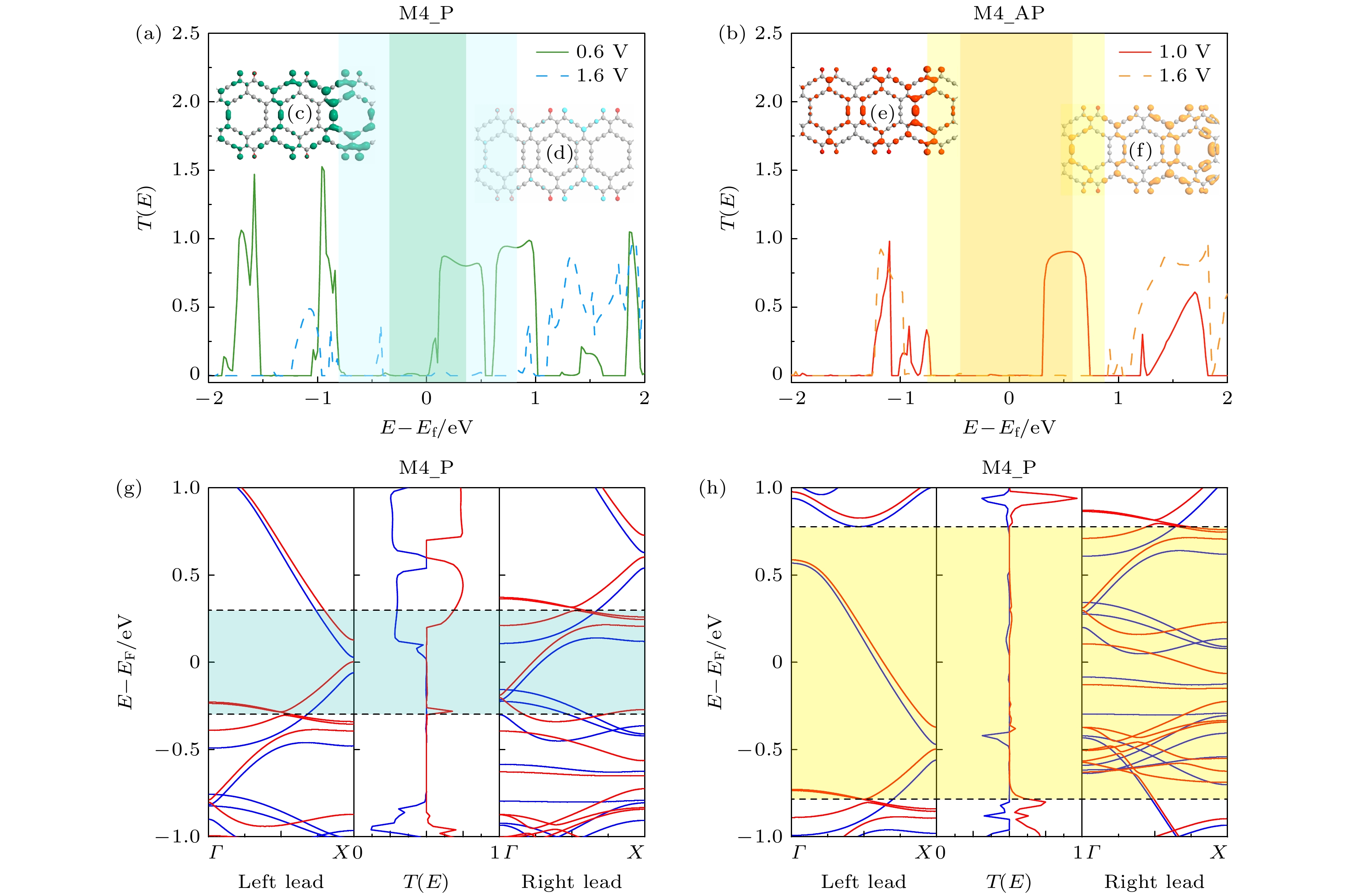
图 7 (a), (b)器件M4在P, AP自旋组态下的透射谱分布图, 实线和虚线分别表示DNR效应中峰值和谷值电压对应的透射谱; (c), (d), (e), (f)在P, AP组态下峰值和谷值时的局域态密度分布图; (g), (h)在P组态下峰值/谷值时的能带结构图和透射谱图, 蓝色和红色实线分别表示SU合SD的自旋方向. 全图中蓝色合黄色阴影区域表示对应的偏压窗.
Figure 7. (a), (b) The transmission spectra of M4 within the P and AP spin configuration, and the solid and dashed lines indicate the transmission spectra corresponding to the peak and valley voltages in the DNR effect; (c), (d), (e), (f) the distributions about the LDOS at peak and valley voltages within the P and AP configurations, respectively; (g), (h) the energy band structures and the transmission spectra of M4 at the peak and valley voltages within P configuration, and blue and red solid lines indicate the SU and SD directions, respectively. The blue and yellow shaded areas on the entire map represent the corresponding bias window.
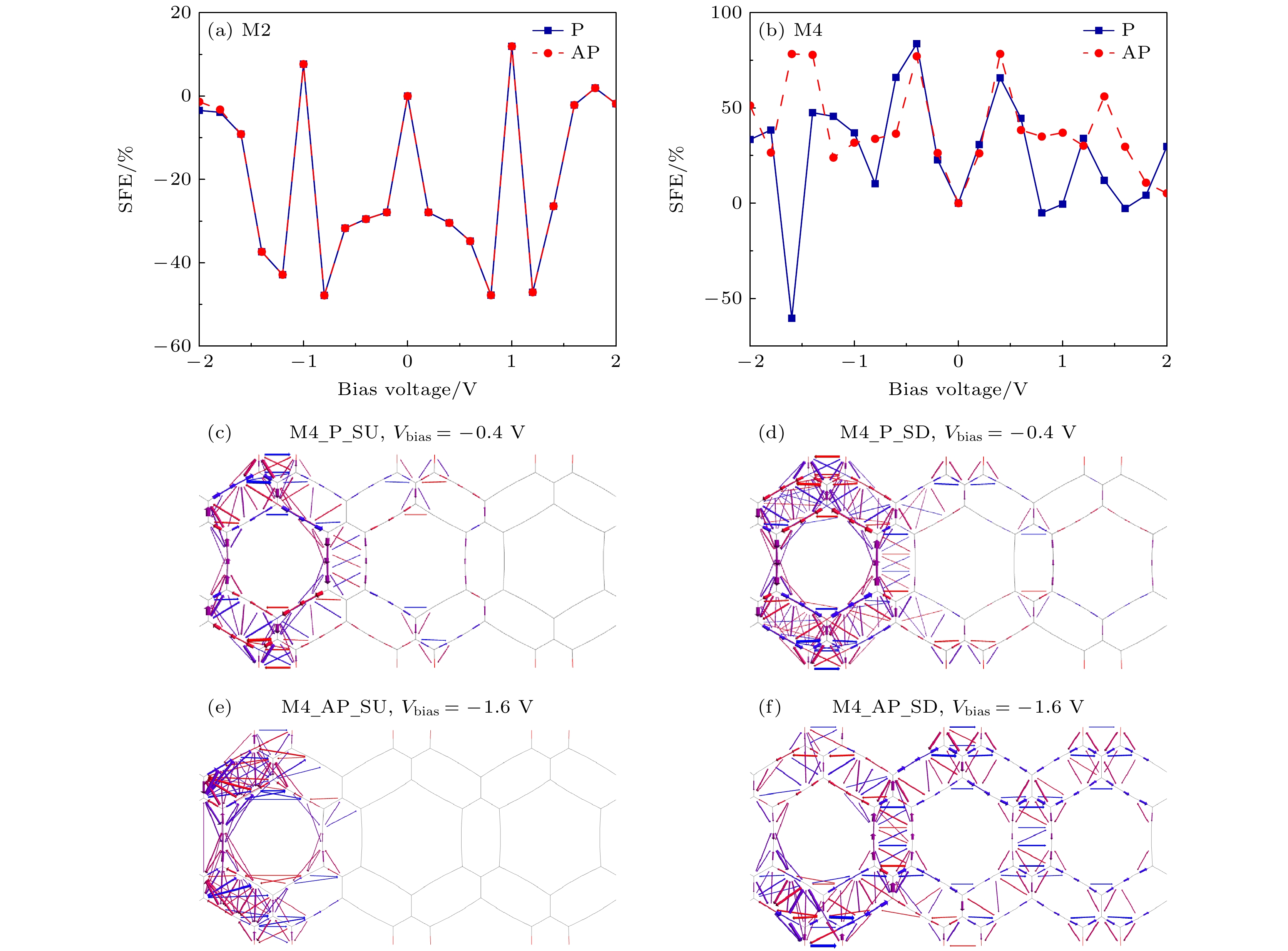
图 8 (a), (b)器件M2, M4的自旋过滤系数随电压变化的曲线图; (c)/(d), (e)/(f)器件M4在P, AP组态下偏置电压为–0.4, –1.6 V时的SU/SD方向的电子传输路径, 蓝色/红色箭头表示电子从左/右移动到右/左电极的传输方向
Figure 8. (a), (b) SFE versus voltage for M2 and M4; (c)/(d), (e)/(f) the electron transport paths for M4 in the SU/SD direction within the P, AP configuration at a bias voltage of –0.4, –1.6 V; the blue/red arrows indicate the direction of the electron transport path from left /right lead to the right/left lead.
-
[1] Ivanovskii A L 2013 Prog. Solid. State. Chem. 41 1
 Google Scholar
[2] Djurišić A B, Li E H 1999 J. Appl. Phys. 85 7404
Google Scholar
[3] Wudl F 2002 J. Mater. Chem. 12 1959
Google Scholar
[4] Ebbesen T W 1996 Phys. Today 49 26
[5] Geim A K, Novoselov K S 2007 Nat. Mater. 6 183
Google Scholar
[6] Narita N, Nagai S, Suzuki S, Nakao K 1998 Phys. Rev. B 58 11009
Google Scholar
[7] Baughman R H, Eckhardt H, Kertesz M 1987 J. Chem. Phys. 87 6687
Google Scholar
[8] Popov V N, Lambin P 2013 Phys. Rev. B 88 075427
Google Scholar
[9] Ni Y, Wang X, Tao W, Zhu S C, Yao K L 2016 Sci. Rep. 6 25914
Google Scholar
[10] Zhang X J, Peng D D, Xie X L, Li X B, Dong Y L, Long M Q 2021 Eur. Phys. J. B 94 86
Google Scholar
[11] Novoselov K S, Geim A K, Morozov S V, Jiang D, Zhang Y, Dubonos S V, Grigorieva I V, Firsov A A 2004 Science 306 666
Google Scholar
[12] Bolotin K I, Sikes K J, Jiang Z, Klima M, Fudenberg G, Hone J, Kim P, Stormer H L 2008 Solid. State. Commun. 146 351
Google Scholar
[13] Alexander B A, Suchismita G, Wen Z B, Irene C, Desalegne T, Feng M, Liu C N 2008 Nano Lett. 8 902
Google Scholar
[14] Li G X, Li Y L, Liu H B, Guo Y B, Li Y J, Zhu D B 2010 Chem. Commun. 46 3256
Google Scholar
[15] Srinivasu K, Ghosh S K 2012 J. Phys. Chem. C. 116 5951
[16] Majidi R 2018 J. Electron. Mater. 47 2890
Google Scholar
[17] Jafari S N, Hakimi Y, Rouhi S 2020 Physica E 119 114022
Google Scholar
[18] Zeng M G, Shen L, Cai Y Q, Sha Z D, Feng Y P 2010 Appl. Phys. Lett. 96 042104
Google Scholar
[19] Ozaki T, Nishio K, Weng H, Kino H 2010 Phys. Rev. B 81 075422
Google Scholar
[20] Dong X S, Chen T, Liu G G, Xie L Z, Zhou G H, Long M Q 2022 ACS Sensors 7 3450
Google Scholar
[21] Li Y, Li X B, Zhang S D, Zhang X J, Long M Q 2022 J. Magn. Magn. Mater. 546 168842
Google Scholar
[22] Chen J, Reed M A, Rawlett A M, Tour J M 1999 Science 286 1550
Google Scholar
[23] Lang N D, Avouris P 1998 Phys. Rev. Lett. 81 3515
Google Scholar
[24] Ding W C, Zhang J, Li X B, Chen T, Zhou G H 2022 Physica E 142 115316
Google Scholar
[25] Huang J, Xu K, Lei S L, Su H B, Yang S F, Li Q X, Yang J L 2012 J. Chem. Phys. 136 064707
Google Scholar
[26] Evlashin S A, Tarkhov M A, Chernodubov D A, Inyushkin A V, Pilevsky A A, Dyakonov P V, Pavlov A A, Suetin N V, Akhatov I S, Perebeinos V 2021 Phys. Rev. Appl. 15 054057
Google Scholar
[27] Peng D D, Zhang X J, Li X B, Wu D, Long M Q 2018 J. Appl. Phys. 124 184303
Google Scholar
[28] Hu J, Ruan X, Chen Y P 2009 Nano. Lett. 9 2730
Google Scholar
[29] Zeng J, Chen K Q 2013 J. Mater. Chem. C 1 4014
Google Scholar
[30] Pan J B, Zhang Z H, Ding K H, Deng X Q, Guo C 2011 Appl. Phys. Lett. 98 092102
Google Scholar
[31] Li J, Zhang Z H, Qiu M, Yuan C, Deng X Q, Fan Z Q, Tang G P, Liang B 2014 Carbon 80 575
Google Scholar
[32] Meyer J C, Girit C O, Crommie M F, Zettl A 2008 Nature 454 319
Google Scholar
[33] Caridad J M, Calogero G, Pedrinazzi P, Santos J E, Impellizzeri A, Gunst T, Booth T J, Sordan R, Bøggild P, Brandbyge M 2018 Nano. Lett. 18 4675
Google Scholar
[34] Saffarzadeh A, Farghadan R 2011 Appl. Phys. Lett. 98 023106
Google Scholar
[35] Mohammadi A, Zaminpayma E 2018 Org. Electron. 61 334
Google Scholar
[36] Zhang L W, Yang Y Q, Chen J, Zheng X H, Zhang L, Xiao L T, Jia S T 2020 Phys. Chem. Chem. Phys. 22 18548
Google Scholar
[37] Bhattacharya B, Sarkar U 2016 J. Phys. Chem. C 120 26793
Google Scholar
[38] Li X B, Zhou J Y, Yu M, Li Y, Zhou K Z, Wang X J, Zhang X J, Long M Q 2023 J. Magn. Magn. Mater. 587 171367
Google Scholar
[39] Chen X, Xu W, Song B, He P 2020 J. Phys. Condens. Matter 32 215501
Google Scholar
[40] Cao L M, Li X B, Li Y, Zhou G H 2020 J. Mater. Chem. C 8 9313
Google Scholar
[41] Perdew J P, Burke K, Ernzerhof M 1996 Phys. Rev. Lett. 77 3865
Google Scholar
[42] Li X B, Cao L M, Long M Q, Liu Z R, Zhou G H 2018 Carbon 131 160
Google Scholar
[43] Wu D, Cao X H, Jia P Z, Zeng Y J, Feng Y X, Tang L M, Zhou W X, Chen K Q 2020 Sci. China-Phys. Mech. Astron. 63 276811
Google Scholar
[44] Ren H, Li Q X, Luo Y, Yang J L 2009 Appl. Phys. Lett. 94 173110
Google Scholar
[45] Li X B, Qi F, Zhao R D, Qiu Z J, Li Y, Long M Q, Zhou G H 2022 J. Mater. Chem. C 10 5292
Google Scholar
[46] 彭淑平, 黄旭东, 刘乾, 任鹏, 伍丹, 范志强 2023 72 058501
Google Scholar
Peng S P, Huang X D, Liu Q, Ren P, Wu D, Fan Z Q 2023 Acta Phys. Sin. 72 058501
Google Scholar
[47] Ding W C, Zhang J, Li X B, Zhou G H 2024 Appl. Surf. Sci. 664 160043
Google Scholar
[48] Yu G L, Ding W C, Xiao X B, Li X B, Zhou G H 2020 Nanoscale. Res. Lett. 15 185
Google Scholar
[49] Zhou Y H, Zeng J, Chen K Q 2014 Carbon 76 175
Google Scholar


 DownLoad:


Metrics
- Abstract views: 368
- PDF Downloads: 3
- Cited By: 0
