-
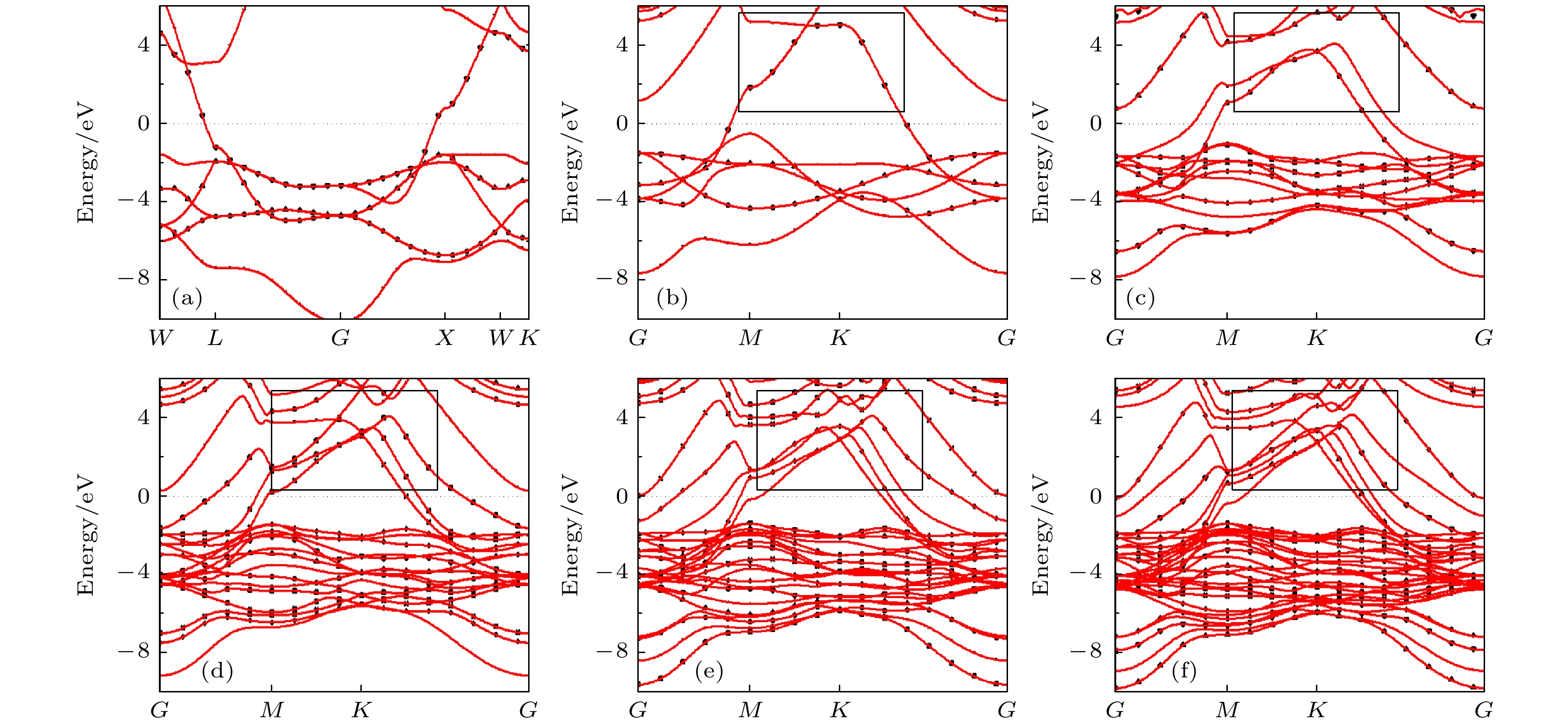
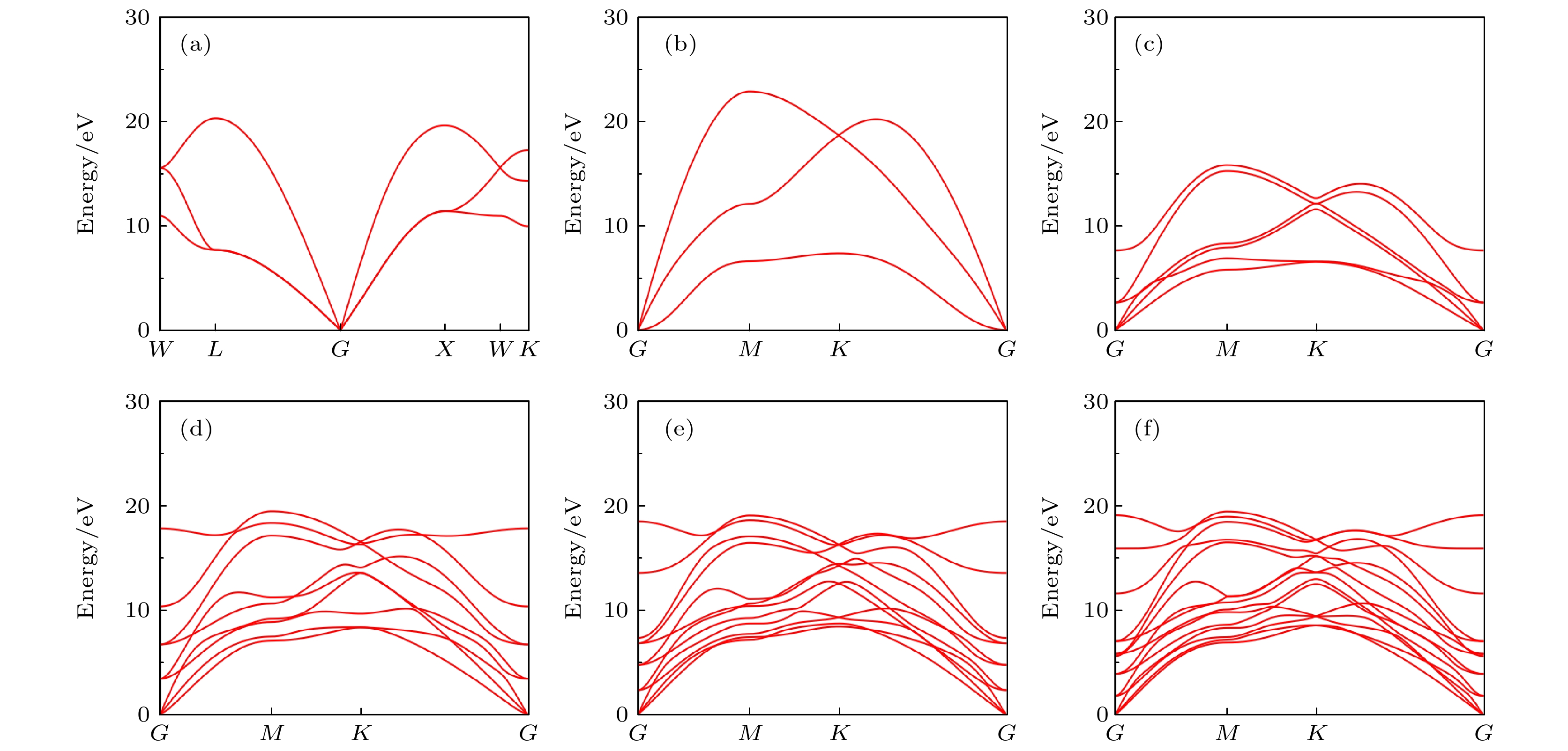
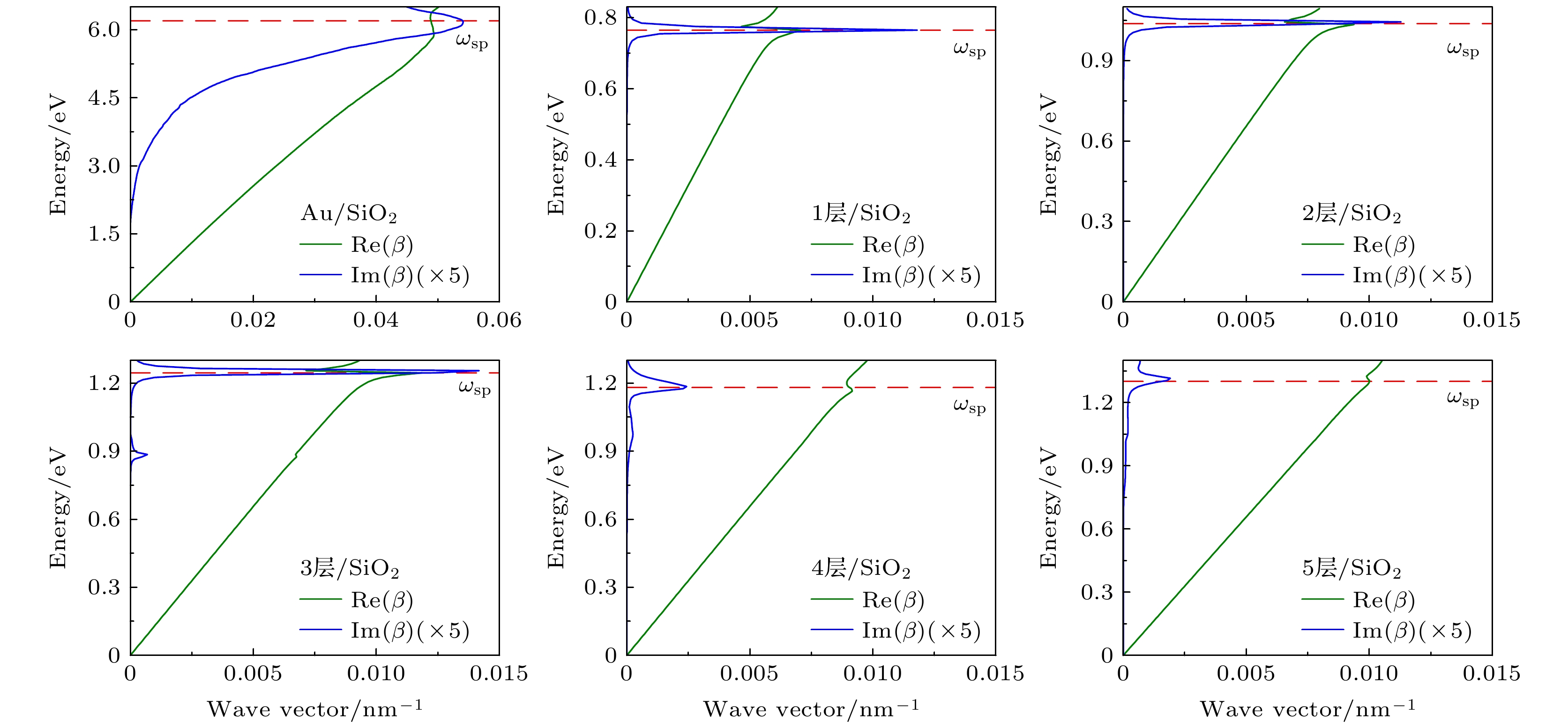
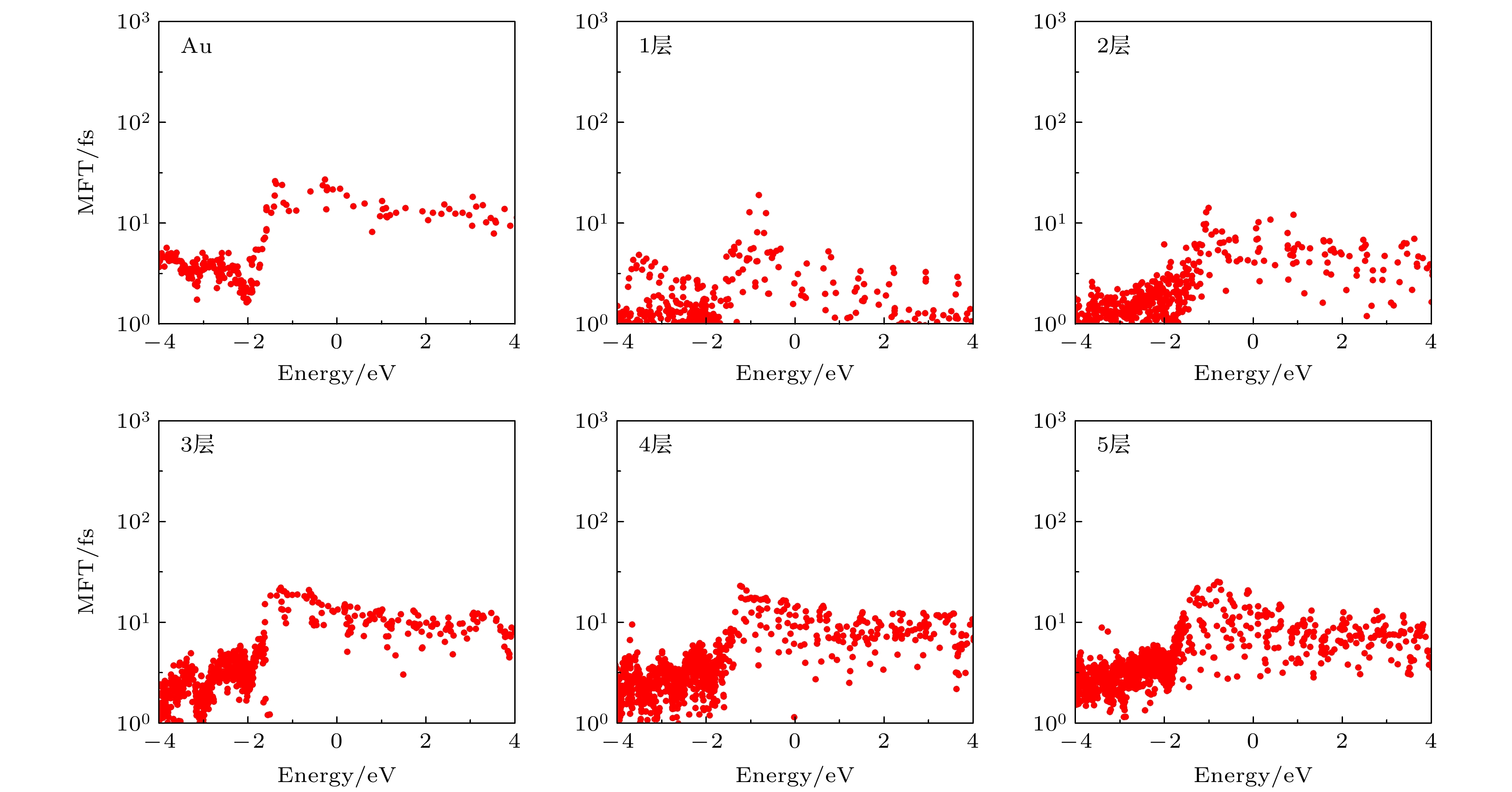
Metal films with a thickness as low as atomic layer have superior light absorption capabilities and conductive properties, especially the surface plasmons excited at the interface between metal film and dielectric can well capture photons and generate hot carriers, making them more efficient in improving the photoelectric conversion efficiency of solar cells, designing photodetectors in the near-infrared band, and sensors based on surface plasmon. However, there is still a lack of systematic theoretical studies on the surface plasmon and hot carrier properties of metal thin films. Based on the many-body first-principles calculation method, in this paper studied systematically are the surface plasmon properties of Au(111) films with thickness in a range from monolayer to 5 monolayers, and the energy distribution and transport properties of hot carriers generated by surface plasmons. The study results show that Au(111) films have low-loss surface plasmon properties. Meanwhile, the surface plasmons excited at the interface between the Au(111) film and the dielectric are strongly confined, which can enhance the local electric field, thus being crucial in nanophotonics applications. In addition, Au(111) film has a high efficiency generating hot carriers , and the generated hot electrons and hot holes are high in energy, and excellent in mean free path and mean free time. Unexpectedly, the direct current conductivity of Au(111) film is significantly better than that of bulk Au. These results provide new ideas and theoretical basis for the design and fabrication of Au(111) films in optoelectronic devices and energy conversion devices.
-
Keywords:
- Au(111) films /
- transport properties /
- surface plasmon /
- hot carriers
[1] Moskovits M 2015 Nat. Nanotechnol. 10 6
 Google Scholar
[2] Kulkarni A P, Noone K M, Munechika K, Guyer S R, Ginger D S 2010 Nano Lett. 10 1501
 Google Scholar
[3] Maier S A 2007 Plasmonics: fundamentals and applications (Bath: Springer) pp177–191
[4] Mukherjee S, Libisch F, Large N, Neumann O, Brown L V, Cheng J, Lassiter J B, Carter E A, Nordlander P, Halas N J 2013 Nano Lett. 13 240
 Google Scholar
[5] Robatjazi H, Bahauddin S M, Doiron C, Thomann I 2015 Nano Lett. 15 6155
 Google Scholar
[6] Christopher P, Xin H L, Linic S 2011 Nat. Chem. 3 467
 Google Scholar
[7] Babicheva V E, Zhukovsky S V, Ikhsanov R S, Protsenko I E, Smetanin I V, Uskov A 2015 ACS Photonics 2 1039
 Google Scholar
[8] Zheng B Y, Zhao H Q, Manjavacas A, McClain M, Nordlander P, Halas N J 2015 Nat. Commun. 6 7797
 Google Scholar
[9] Leenheer A J, Narang P, Lewis N S, Atwater H A 2014 J. Appl. Phys. 115 134301
 Google Scholar
[10] Maniyara R A, Rodrigo D, Yu R, Canet-Ferrer J, Ghosh D S R, Yongsunthon R, Baker D E, Rezikyan A, de Abajo F J G, Pruneri V 2019 Nat. Photonics 13 328
 Google Scholar
[11] Xue X T, Fan Y H, Segal E, Wang W P, Yang F, Wang Y F, Zhao F T, Fu W Y, Ling Y H, Salomon A, Zhang Z 2021 Mater. Today 46 54
 Google Scholar
[12] Mandal P, Sharma S 2016 Renewable Sustainable Energy Rev. 65 537
 Google Scholar
[13] Zhang C, Guney D O, Pearce J M 2016 Mater. Res. Express 3 105034
 Google Scholar
[14] Li Z J, Lü W, Zhang C, Qin J W, Wei W, Shao J J, Wang D W, Li B H, Kang F Y, Yang Q H 2014 Nanoscale 6 9554
 Google Scholar
[15] Shahjamali M M, Salvador M, Bosman M, Ginger D S, Xue C 2014 J. Phys. Chem. C 118 12459
 Google Scholar
[16] Tsysar K M, Andreev V G, Vdovin V A 2016 International Conference on Micro- and Nano-Electronics 2016 Zvenigorod, Russia, October 3-7, 2016 pp40–45
[17] Shipway A N, Katz E, Willner I 2000 ChemPhysChem 1 18
 Google Scholar
[18] 初凤红, 蔡海文, 瞿荣辉, 方祖捷 2009 激光与光电子进展 46 58
Chu F H, Cai H W, Qu R H, Fang Z J 2009 Laser Optoelectron. Prog. 46 58
[19] Zhu Q, Hong Y, Cao G, Zhang Y, Wang J W 2020 ACS Nano 14 17091
 Google Scholar
[20] Forti S, Link S, Sthr A, Niu Y, Zakharov A A, Coletti C, Starke U 2020 Nat. Commun. 11 2236
 Google Scholar
[21] Sundararaman R, Letchworth-Weaver K, Schwarz K A, Gunceler D, Ozhabes Y, Arias T A 2017 Softwarex 6 278
 Google Scholar
[22] Perdew J P, Ruzsinszky A, Csonka G I, Vydrov O A, Scuseria G E, Constantin L A, Zhou X L, Burke K 2009 Phys. Rev. Lett. 102 136406
 Google Scholar
[23] Dudarev S L, Botton G A, Savrasov S Y, Humphreys C J, Sutton A P 1998 Phys. Rev. B 57 1505
 Google Scholar
[24] Brown A M, Sundararaman R, Narang P, Goddard W A, Atwater H A 2016 ACS Nano 10 957
 Google Scholar
[25] Marzari N, Vanderbilt D 1997 Phys. Rev. B 56 12847
 Google Scholar
[26] Giustino F, Cohen M L, Louie S G 2007 Phys. Rev. B 76 165108
 Google Scholar
[27] Sundararaman R, Christensen T, Ping Y, Rivera N, Joannopoulos J D, Soljacic M, Narang P 2020 Phys. Rev. Mater. 4 074011
 Google Scholar
[28] Jian C C, Ma X C, Zhang J Q, Jiang J L 2022 Nanophotonics 11 531
 Google Scholar
[29] Habib A, Florio F, Sundararaman R 2018 J. Opt. 20 064001
 Google Scholar
[30] Shore K, Chan D 1990 Electron. Lett. 26 1206
 Google Scholar
[31] Kolwas K, Derkachova A 2020 Nanomaterials 10 1411
 Google Scholar
[32] Laref S, Cao J, Asaduzzaman A, Runge K, Deymier P, Ziolkowski R W, Miyawaki M, Muralidharan K 2013 Opt. Express 21 11827
 Google Scholar
[33] Jian C C, Ma X C, Zhang J Q, Yong X 2021 J. Phys. Chem. C 125 15185
 Google Scholar
[34] Bernardi M, Vigil-Fowler D, Lischner J, Neaton J B, Louie S G 2014 Phys. Rev. Lett. 112 257402
 Google Scholar
[35] Bernardi M, Vigil-Fowler D, Ong C S, Neaton J B, Louie S G 2015 Proc. Natl. Acad. Sci. U. S. A. 112 5291
 Google Scholar
[36] Bernardi M, Mustafa J, Neaton J B, Louie S G 2015 Nat. Commun. 6 7044
 Google Scholar
[37] Bauer R, Schmid A, Pavone P, Strauch D 1998 Phys. Rev. B 57 11276
 Google Scholar
[38] Giri A, Gaskins J T, Li L Q, Wang Y S, Prezhdo O V, Hopkins P E 2019 Phys. Rev. B 99 165139
 Google Scholar
[39] Allen P 1971 Phys. Rev. B 3 305
 Google Scholar
[40] Rangel T, Kecik D, Trevisanutto P E, Rignanese G M, Van Swygenhoven H, Olevano V 2012 Phys. Rev. B 86 125125
 Google Scholar
[41] Xu M, Yang J Y, Zhang S Y, Liu L H 2017 Phys. Rev. B 96 115154
 Google Scholar
[42] Ma X C, Sun H, Wang Y C, Wu X, Zhang J Q 2018 Nano Energy 53 932
 Google Scholar
[43] Wang Y, Chen L Y, Xu B, Zheng W M, Zhang R J, Qian D L, Zhou S M, Zheng Y X, Dai N, Yang Y M, Ding K B, Zhang X M 1998 Thin Solid Films 313 232
[44] Zhang Z Y, Wang H Y, Du J L, Zhang X L, Hao Y W, Chen Q D, Sun H B 2015 IEEE Photonics Technol. Lett. 27 821
 Google Scholar
[45] Jablan M, Soljacic M, Buljan H 2013 Proc. IEEE 101 1689
 Google Scholar
[46] Jian C C, Zhang J Q, He W M, Ma X C 2021 Nano Energy 82 105763
 Google Scholar
[47] Khurgin J B 2015 Nat. Nanotechnol. 10 2
 Google Scholar
[48] Brongersma M L, Halas N J, Nordlander P 2015 Nat. Nanotechnol. 10 25
 Google Scholar
[49] Bernardi M, Mustafa J, Neaton J B, Louie S G 2015 Nature Communications 6 7044
[50] Gladskikh I A, Leonov N B, Przhibel'skii S G, Vartanyan T A 2014 J. Opt. Technol. 81 280
 Google Scholar
[51] Antonets I V, Kotov L N, Nekipelov S V, Golubev Y A 2004 Tech. Phys. 49 306
 Google Scholar
[52] Robert C W, Melvin J A, William H B 2003 CRC Handbook of Chemistry and Physics (84th Ed.) (Florida: Boca Raton) pp13–14
-
图 1 (a) Au面心立方结构; (b) 计算块体Au电子结构使用的原胞; (c) 块体Au的第一布里渊区, 其能带结构和声子谱沿
$k$ 点路径W-L-G-X-W-K计算; (d) Au(111)薄膜按照“膜按照“方式堆积示意图; (e) Au(111)薄膜的第一布里渊区, 其能带结构和声子谱沿$k$ 点路径G-M-K-G计算Figure 1. (a) Face-centered cubic structure of Au; (b) the primitive cell used to calculate the electronic structure of bulk Au; (c) the first Brillouin zone of bulk Au, and the irreducible k-point path W-L-G-X-W-K is used for calculating its band structure and phonon spectra; (d) Au(111) films stacked in "ABC" manner; (e) the first Brillouin zone of Au(111) films, the irreducible k-point path G-M-K-G is used for calculating its band structure and phonon spectra.
图 4 介电函数虚部 (a) 块体Au的Johnson实验测量结果和DFT理论计算结果; (b) 块体Au和1—5层Au(111)薄膜
Figure 4. (a) The imaginary part of the dielectric function of Johnson experimental measurement result and DFT theoretical calculation result of bulk Au; (b) the imaginary part of the dielectric function of bulk Au and Au(111) films with thickness from 1 to 5 atomic layers.
图 13 (a) 块体Au和1—5层Au(111)薄膜在0—500 K温度范围内的直流电导率; (b) 块体Au和(c) 1—5层Au(111)薄膜加权传输Eliashberg谱函数
$ \alpha _v^2 F\left( \omega \right) $ Figure 13. (a) DC conductivity of bulk Au and Au(111) films with thickness from 1 to 5 atomic layers in the temperature range of 0–500 K, the transport-weighted Eliashberg spectral function of (b) bulk Au and (c) Au(111) films with thickness from 1 to 5 atomic layers.
表 1 传输常数
$\lambda $ Table 1. The transport constant
$\lambda $ .块体Au 1层 2层 3层 4层 5层 $\lambda $ 629.52 10.24 18.27 8.85 7.75 6.39 表 2 费米速度
${\nu _{\rm{F}}}$ Table 2. The Fermi velocity
${\nu _{\rm{F}}}$ .块体Au 1层 2层 3层 4层 5层 ${\nu _F}$ 0.62 0.68 0.51 0.50 0.49 0.48 -
[1] Moskovits M 2015 Nat. Nanotechnol. 10 6
 Google Scholar
[2] Kulkarni A P, Noone K M, Munechika K, Guyer S R, Ginger D S 2010 Nano Lett. 10 1501
 Google Scholar
[3] Maier S A 2007 Plasmonics: fundamentals and applications (Bath: Springer) pp177–191
[4] Mukherjee S, Libisch F, Large N, Neumann O, Brown L V, Cheng J, Lassiter J B, Carter E A, Nordlander P, Halas N J 2013 Nano Lett. 13 240
 Google Scholar
[5] Robatjazi H, Bahauddin S M, Doiron C, Thomann I 2015 Nano Lett. 15 6155
 Google Scholar
[6] Christopher P, Xin H L, Linic S 2011 Nat. Chem. 3 467
 Google Scholar
[7] Babicheva V E, Zhukovsky S V, Ikhsanov R S, Protsenko I E, Smetanin I V, Uskov A 2015 ACS Photonics 2 1039
 Google Scholar
[8] Zheng B Y, Zhao H Q, Manjavacas A, McClain M, Nordlander P, Halas N J 2015 Nat. Commun. 6 7797
 Google Scholar
[9] Leenheer A J, Narang P, Lewis N S, Atwater H A 2014 J. Appl. Phys. 115 134301
 Google Scholar
[10] Maniyara R A, Rodrigo D, Yu R, Canet-Ferrer J, Ghosh D S R, Yongsunthon R, Baker D E, Rezikyan A, de Abajo F J G, Pruneri V 2019 Nat. Photonics 13 328
 Google Scholar
[11] Xue X T, Fan Y H, Segal E, Wang W P, Yang F, Wang Y F, Zhao F T, Fu W Y, Ling Y H, Salomon A, Zhang Z 2021 Mater. Today 46 54
 Google Scholar
[12] Mandal P, Sharma S 2016 Renewable Sustainable Energy Rev. 65 537
 Google Scholar
[13] Zhang C, Guney D O, Pearce J M 2016 Mater. Res. Express 3 105034
 Google Scholar
[14] Li Z J, Lü W, Zhang C, Qin J W, Wei W, Shao J J, Wang D W, Li B H, Kang F Y, Yang Q H 2014 Nanoscale 6 9554
 Google Scholar
[15] Shahjamali M M, Salvador M, Bosman M, Ginger D S, Xue C 2014 J. Phys. Chem. C 118 12459
 Google Scholar
[16] Tsysar K M, Andreev V G, Vdovin V A 2016 International Conference on Micro- and Nano-Electronics 2016 Zvenigorod, Russia, October 3-7, 2016 pp40–45
[17] Shipway A N, Katz E, Willner I 2000 ChemPhysChem 1 18
 Google Scholar
[18] 初凤红, 蔡海文, 瞿荣辉, 方祖捷 2009 激光与光电子进展 46 58
Chu F H, Cai H W, Qu R H, Fang Z J 2009 Laser Optoelectron. Prog. 46 58
[19] Zhu Q, Hong Y, Cao G, Zhang Y, Wang J W 2020 ACS Nano 14 17091
 Google Scholar
[20] Forti S, Link S, Sthr A, Niu Y, Zakharov A A, Coletti C, Starke U 2020 Nat. Commun. 11 2236
 Google Scholar
[21] Sundararaman R, Letchworth-Weaver K, Schwarz K A, Gunceler D, Ozhabes Y, Arias T A 2017 Softwarex 6 278
 Google Scholar
[22] Perdew J P, Ruzsinszky A, Csonka G I, Vydrov O A, Scuseria G E, Constantin L A, Zhou X L, Burke K 2009 Phys. Rev. Lett. 102 136406
 Google Scholar
[23] Dudarev S L, Botton G A, Savrasov S Y, Humphreys C J, Sutton A P 1998 Phys. Rev. B 57 1505
 Google Scholar
[24] Brown A M, Sundararaman R, Narang P, Goddard W A, Atwater H A 2016 ACS Nano 10 957
 Google Scholar
[25] Marzari N, Vanderbilt D 1997 Phys. Rev. B 56 12847
 Google Scholar
[26] Giustino F, Cohen M L, Louie S G 2007 Phys. Rev. B 76 165108
 Google Scholar
[27] Sundararaman R, Christensen T, Ping Y, Rivera N, Joannopoulos J D, Soljacic M, Narang P 2020 Phys. Rev. Mater. 4 074011
 Google Scholar
[28] Jian C C, Ma X C, Zhang J Q, Jiang J L 2022 Nanophotonics 11 531
 Google Scholar
[29] Habib A, Florio F, Sundararaman R 2018 J. Opt. 20 064001
 Google Scholar
[30] Shore K, Chan D 1990 Electron. Lett. 26 1206
 Google Scholar
[31] Kolwas K, Derkachova A 2020 Nanomaterials 10 1411
 Google Scholar
[32] Laref S, Cao J, Asaduzzaman A, Runge K, Deymier P, Ziolkowski R W, Miyawaki M, Muralidharan K 2013 Opt. Express 21 11827
 Google Scholar
[33] Jian C C, Ma X C, Zhang J Q, Yong X 2021 J. Phys. Chem. C 125 15185
 Google Scholar
[34] Bernardi M, Vigil-Fowler D, Lischner J, Neaton J B, Louie S G 2014 Phys. Rev. Lett. 112 257402
 Google Scholar
[35] Bernardi M, Vigil-Fowler D, Ong C S, Neaton J B, Louie S G 2015 Proc. Natl. Acad. Sci. U. S. A. 112 5291
 Google Scholar
[36] Bernardi M, Mustafa J, Neaton J B, Louie S G 2015 Nat. Commun. 6 7044
 Google Scholar
[37] Bauer R, Schmid A, Pavone P, Strauch D 1998 Phys. Rev. B 57 11276
 Google Scholar
[38] Giri A, Gaskins J T, Li L Q, Wang Y S, Prezhdo O V, Hopkins P E 2019 Phys. Rev. B 99 165139
 Google Scholar
[39] Allen P 1971 Phys. Rev. B 3 305
 Google Scholar
[40] Rangel T, Kecik D, Trevisanutto P E, Rignanese G M, Van Swygenhoven H, Olevano V 2012 Phys. Rev. B 86 125125
 Google Scholar
[41] Xu M, Yang J Y, Zhang S Y, Liu L H 2017 Phys. Rev. B 96 115154
 Google Scholar
[42] Ma X C, Sun H, Wang Y C, Wu X, Zhang J Q 2018 Nano Energy 53 932
 Google Scholar
[43] Wang Y, Chen L Y, Xu B, Zheng W M, Zhang R J, Qian D L, Zhou S M, Zheng Y X, Dai N, Yang Y M, Ding K B, Zhang X M 1998 Thin Solid Films 313 232
[44] Zhang Z Y, Wang H Y, Du J L, Zhang X L, Hao Y W, Chen Q D, Sun H B 2015 IEEE Photonics Technol. Lett. 27 821
 Google Scholar
[45] Jablan M, Soljacic M, Buljan H 2013 Proc. IEEE 101 1689
 Google Scholar
[46] Jian C C, Zhang J Q, He W M, Ma X C 2021 Nano Energy 82 105763
 Google Scholar
[47] Khurgin J B 2015 Nat. Nanotechnol. 10 2
 Google Scholar
[48] Brongersma M L, Halas N J, Nordlander P 2015 Nat. Nanotechnol. 10 25
 Google Scholar
[49] Bernardi M, Mustafa J, Neaton J B, Louie S G 2015 Nature Communications 6 7044
[50] Gladskikh I A, Leonov N B, Przhibel'skii S G, Vartanyan T A 2014 J. Opt. Technol. 81 280
 Google Scholar
[51] Antonets I V, Kotov L N, Nekipelov S V, Golubev Y A 2004 Tech. Phys. 49 306
 Google Scholar
[52] Robert C W, Melvin J A, William H B 2003 CRC Handbook of Chemistry and Physics (84th Ed.) (Florida: Boca Raton) pp13–14
Catalog
Metrics
- Abstract views: 6732
- PDF Downloads: 156
- Cited By: 0


 DownLoad:


