-
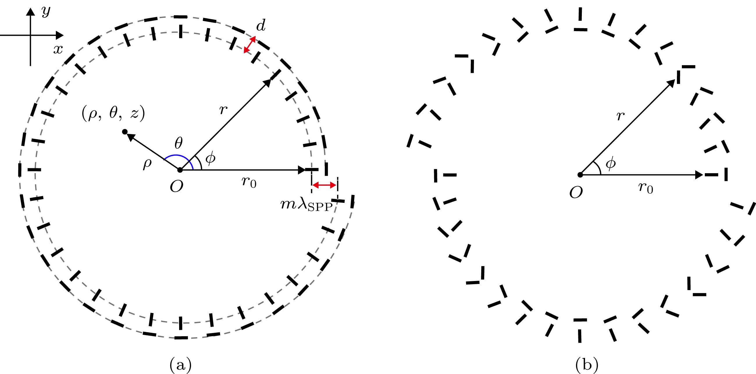
Surface plasmon polariton (SPP) is an electromagnetic oscillation which is produced by the interaction of free electrons on metal surface with incident light field. Using some specific metal metasurface structures, plasmonic vortices can be easily obtained. The SPP can well confine the light field within the interface between metal and medium. The SPP has two excellent characteristics: the ability to break through the diffraction limit and the strong field enhancing effect. Consequently, it has unique advantages in many applications, such as nanoparticle trapping, near-field imaging and sensing. The key point lies in selecting the incident light and the construction of metasurface structure when we want to produce SPP vortices. Especially the construction of metasurface structure has great influence on the generation of SPP vortices. So far, many structures have been proposed to produce SPP vortices. In 2015, Byoungho Lee research group (Lee S Y, Kim S J, Kwon H, Lee B 2015 IEEE Photonics Technol. Lett. 27 705) designed a structure of double-ring distributed nanoslits which can produce high-order plasmonic vortices by circularly polarized light. In addition, the use of Archimedes slit structure to generate optical vortices is currently a more common method. More recently, a novel plasmonic vortex lens was proposed to produce SPP vortices with arbitrary topological charges. The plasmonic vortex lens consists of an array of gold film nanoslits, and the superposing of the SPP field excited by each nanoslit can produce a composite plasmonic vortex. Here, we propose a novel spiral metasurface structure for generating surface plasmonic vortices. Using the combination of theoretical analysis and finite difference time domain (FDTD) simulation, we find that the topological charge quantity of surface plasmon vortices can be changed by adjusting five parameters, namely, the chirality of incident circularly polarized light, the difference in radius between inner and outer nanocavity array, the rotational velocity factor of nanocavity array, the number of segments of spiral, and the pitch of spiral. This metasurface structure has many adjustable parameters and each parameter can influence the final surface plasmon vortices. Therefore, the plasmonic vortices with an arbitrary topological charge quantity can be generated and manipulated simply by using such a metasurface structure. This work can be expected to have a very broad prospect of applications in super resolution microscopy, quantum cryptography, nanoparticle manipulation, optical data storage, and optical communication. -
Keywords:
- metasurface structure /
- surface plasmon polariton /
- optical vortices /
- topological charges
[1] Maier S A 2007 Plasmonics: Fundamentals and applications (Berlin: Springer) pp49–52
[2] Fang N, Lee H, Sun C, Zhang X 2005 Science 308 534
 Google Scholar
[3] Luo X G, Ishihara T 2004 Opt. Express 12 3055
 Google Scholar
[4] Langhammer C, Larsson E M, Kasemo B, Zoric I 2010 Nano Lett. 10 3529
 Google Scholar
[5] Nie S, Emory S R 1997 Science 275 1102
 Google Scholar
[6] Wurtz G A, Pollard R, Zayats A V 2006 Phys. Rev. Lett. 97 057402
 Google Scholar
[7] Allen L, Beijersbergen M W, Spreeuw R J C, Woerdman J P 1992 Phys. Rev. A 45 8185
 Google Scholar
[8] Yang Y J, Thirunavukkarasu G, Babiker M, Yuan J 2017 Phys. Rev. Lett. 119 094802
 Google Scholar
[9] Chen C F, Ku C T, Tai Y H, Wei P K, Lin H N, Huang C B 2015 Nano Lett. 15 2746
 Google Scholar
[10] Yu N F, Genevet P, Kats M A, Aieta F, Tetienne J P, Capasso F, Gaburro Z 2011 Science 334 333
 Google Scholar
[11] Vedantam S, Lee H, Tang J, Conway J, Staffaroni M, Yablonovitch E 2009 Nano Lett. 9 3447
 Google Scholar
[12] Gorodetski Y, Niv A, Kleiner V, Hasman E 2008 Phys. Rev. Lett. 101 043903
 Google Scholar
[13] 李嘉明, 唐鹏, 王佳见, 黄涛, 林峰, 方哲宇, 朱星 2015 64 194201
 Google Scholar
Li J M, Tang P, Wang J J, Huang T, Lin F, Fang Z Y, Zhu X 2015 Acta Phys. Sin. 64 194201
 Google Scholar
[14] Lee S Y, Kim S J, Kwon H, Lee B 2015 IEEE Photonics Technol. Lett. 27 705
 Google Scholar
[15] Tang B J, Zhang B F, Ding J P 2019 Appl. Opt. 58 833
 Google Scholar
[16] Hell S W, Wichmann J 1994 Opt. Lett. 19 780
 Google Scholar
[17] Vallone G, D’AmbrosioV, Sponselli A, Slussarenko S, Marrucci L, Sciarrino F, Villoresi P 2014 Phys. Rev. Lett. 113 060503
 Google Scholar
[18] Hong Z Y, Zhang J, Drinkwater B W 2015 Phys. Rev. Lett. 114 214301
 Google Scholar
[19] Marzo A, Caleap M, Drinkwater B W 2018 Phys. Rev. Lett. 120 044301
 Google Scholar
[20] Tsai W Y, Huang J S, Huang C B 2014 Nano Lett. 14 547
 Google Scholar
[21] Ding D S, Zhou Z Y, Shi B S, Guo G C 2013 Nat. Commun. 4 2527
 Google Scholar
[22] Nicolas A, Veissier L, Giner L, Giacobino E 2014 Nat. Photonics 8 234
 Google Scholar
[23] Wang J, Yang J Y, Fazal I M, Ahmed N 2012 Nat. Photonics 6 488
 Google Scholar
[24] Bozinovic N, Yue Y, Ren Y X, Tur M 2013 Science 340 1545
 Google Scholar
[25] Rui G H, Zhan Q W, Cui Y P 2015 Sci. Rep. 5 13732
 Google Scholar
[26] Yang S Y, Chen W B, Nelson R L, Zhan Q W 2009 Opt. Lett. 34 3048
-
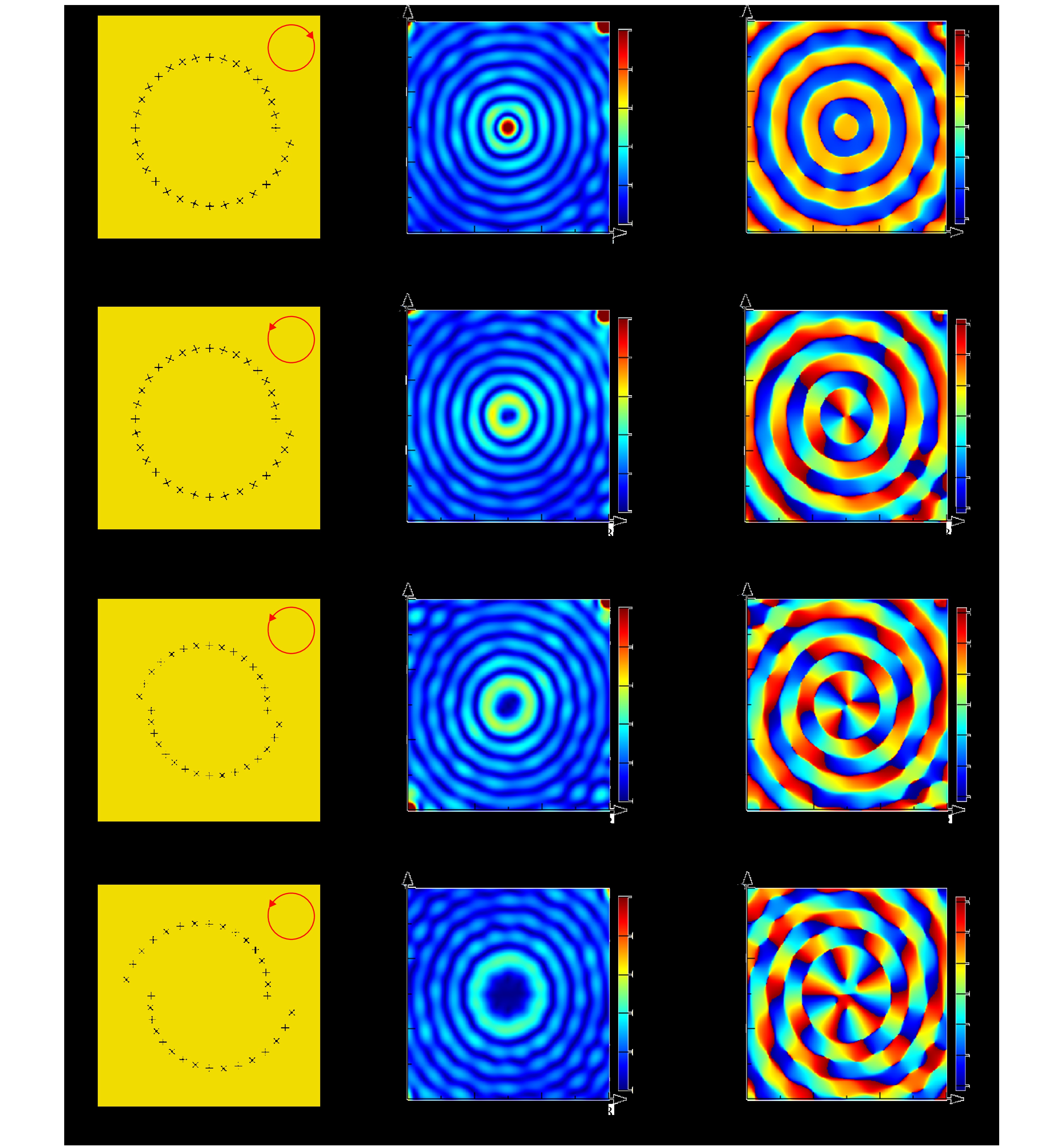
图 2 内外两层螺线之间的距离
$d = 0$ 时的结构示意图、电场强度以及相位分布图 (a)−(c)$\sigma=- 1$ ; (d)−(f)$\sigma=1$ ; (g)−(i)$\sigma=1$ ; (j)−(l)$\sigma=1$ Figure 2. The obtained electric field intensity and phase distribution when distance between inner and outer spirals is equal to 0: (a)−(c)
$\sigma=- 1$ ; (d)−(f)$\sigma=1$ ; (g)−(i)$\sigma=1$ ; (j)−(l)$\sigma=1$ .图 3 内外两层螺线之间的距离
$d = {\lambda _{\rm SPP}}/2$ 时的结构示意图、电场强度以及相位分布图 (a)−(c)$\sigma = - 1$ ; (d)−(f)$\sigma = - 1$ ; (g)−(i)$\sigma = 1$ ; (j)−(l)$\sigma = 1$ ; (m)−(o)$\sigma = 1$ Figure 3. The obtained electric field intensity and phase distribution when distance between inner and outer spirals is equal to
${\lambda _{\rm SPP}}/2$ : (a)−(c)$\sigma = - 1$ ; (d)−(f)$\sigma = - 1$ ; (g)−(i)$\sigma = 1$ ; (j)−(l)$\sigma = 1$ ; (m)−(o)$\sigma = 1$ . -
[1] Maier S A 2007 Plasmonics: Fundamentals and applications (Berlin: Springer) pp49–52
[2] Fang N, Lee H, Sun C, Zhang X 2005 Science 308 534
 Google Scholar
[3] Luo X G, Ishihara T 2004 Opt. Express 12 3055
 Google Scholar
[4] Langhammer C, Larsson E M, Kasemo B, Zoric I 2010 Nano Lett. 10 3529
 Google Scholar
[5] Nie S, Emory S R 1997 Science 275 1102
 Google Scholar
[6] Wurtz G A, Pollard R, Zayats A V 2006 Phys. Rev. Lett. 97 057402
 Google Scholar
[7] Allen L, Beijersbergen M W, Spreeuw R J C, Woerdman J P 1992 Phys. Rev. A 45 8185
 Google Scholar
[8] Yang Y J, Thirunavukkarasu G, Babiker M, Yuan J 2017 Phys. Rev. Lett. 119 094802
 Google Scholar
[9] Chen C F, Ku C T, Tai Y H, Wei P K, Lin H N, Huang C B 2015 Nano Lett. 15 2746
 Google Scholar
[10] Yu N F, Genevet P, Kats M A, Aieta F, Tetienne J P, Capasso F, Gaburro Z 2011 Science 334 333
 Google Scholar
[11] Vedantam S, Lee H, Tang J, Conway J, Staffaroni M, Yablonovitch E 2009 Nano Lett. 9 3447
 Google Scholar
[12] Gorodetski Y, Niv A, Kleiner V, Hasman E 2008 Phys. Rev. Lett. 101 043903
 Google Scholar
[13] 李嘉明, 唐鹏, 王佳见, 黄涛, 林峰, 方哲宇, 朱星 2015 64 194201
 Google Scholar
Li J M, Tang P, Wang J J, Huang T, Lin F, Fang Z Y, Zhu X 2015 Acta Phys. Sin. 64 194201
 Google Scholar
[14] Lee S Y, Kim S J, Kwon H, Lee B 2015 IEEE Photonics Technol. Lett. 27 705
 Google Scholar
[15] Tang B J, Zhang B F, Ding J P 2019 Appl. Opt. 58 833
 Google Scholar
[16] Hell S W, Wichmann J 1994 Opt. Lett. 19 780
 Google Scholar
[17] Vallone G, D’AmbrosioV, Sponselli A, Slussarenko S, Marrucci L, Sciarrino F, Villoresi P 2014 Phys. Rev. Lett. 113 060503
 Google Scholar
[18] Hong Z Y, Zhang J, Drinkwater B W 2015 Phys. Rev. Lett. 114 214301
 Google Scholar
[19] Marzo A, Caleap M, Drinkwater B W 2018 Phys. Rev. Lett. 120 044301
 Google Scholar
[20] Tsai W Y, Huang J S, Huang C B 2014 Nano Lett. 14 547
 Google Scholar
[21] Ding D S, Zhou Z Y, Shi B S, Guo G C 2013 Nat. Commun. 4 2527
 Google Scholar
[22] Nicolas A, Veissier L, Giner L, Giacobino E 2014 Nat. Photonics 8 234
 Google Scholar
[23] Wang J, Yang J Y, Fazal I M, Ahmed N 2012 Nat. Photonics 6 488
 Google Scholar
[24] Bozinovic N, Yue Y, Ren Y X, Tur M 2013 Science 340 1545
 Google Scholar
[25] Rui G H, Zhan Q W, Cui Y P 2015 Sci. Rep. 5 13732
 Google Scholar
[26] Yang S Y, Chen W B, Nelson R L, Zhan Q W 2009 Opt. Lett. 34 3048
Catalog
Metrics
- Abstract views: 10404
- PDF Downloads: 225
- Cited By: 0


 DownLoad:


