-
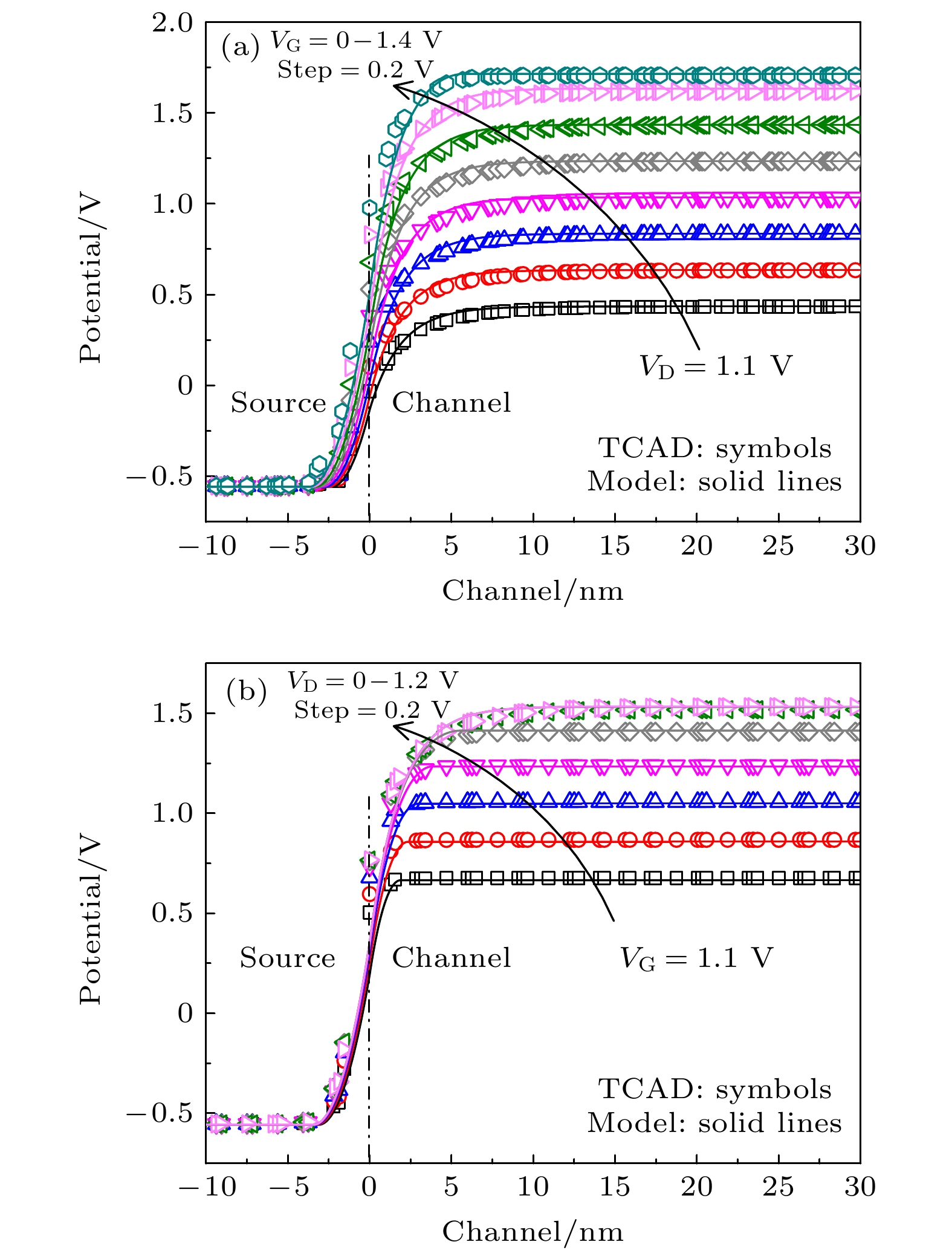
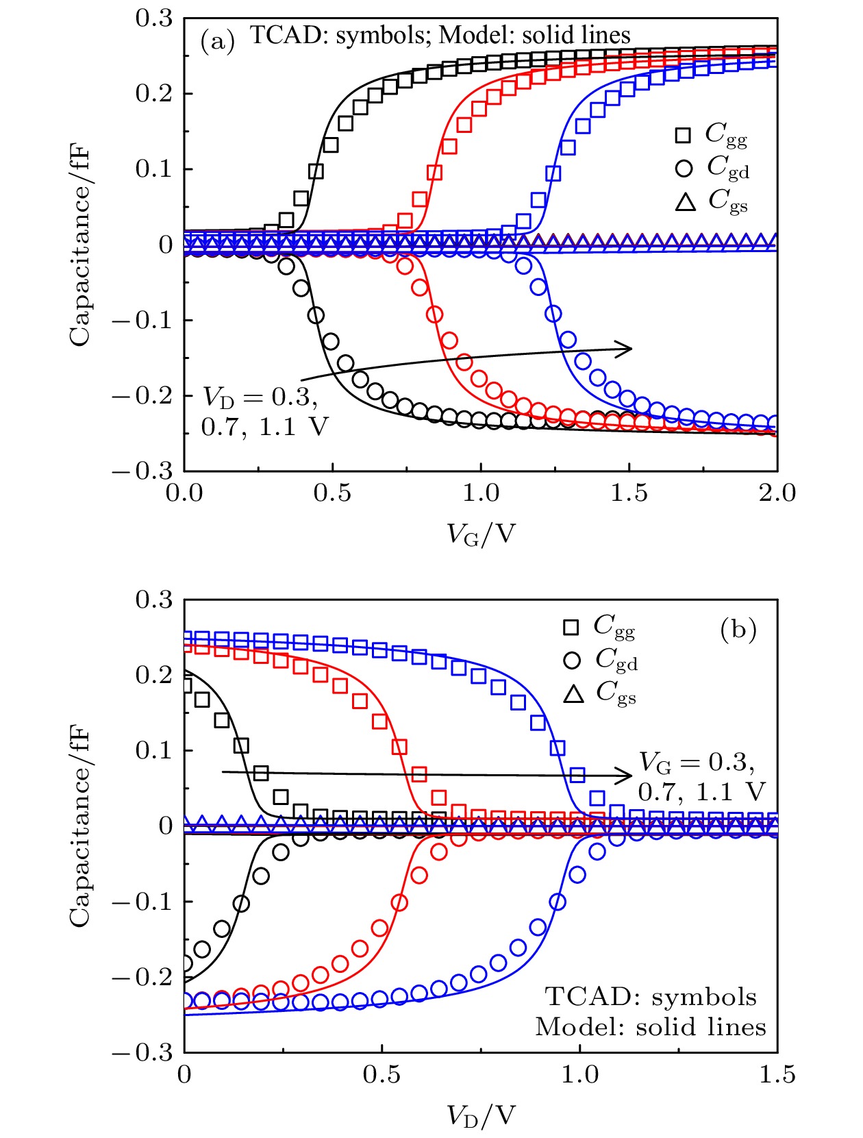
The nanowire gate-all-around (GAA) structures with the nearly ultimate channel electrostatic integrity of the gate field can exhibit the best immunity to the short channel effect and drain-induced barrier lowering. Moreover, owing to the enhanced control efficiency of gate over the tunneling junction, the GAA-TFET also gives improved subthreshold swing and on-state current. Despite the excellent device performance, an accurate model is very significant for the practical application. Compared with the numerical methods which are usually time consuming and computationally inefficient, an analytical model could accelerate the device investigation and circuit design process. Even though some tunneling current models have already been reported for nanowire tunneling field-effect-transistors (TFETs), the model of the terminal capacitance is still an issue for nanowire TFETs. The capacitance is of great significance for the transient simulation. In this paper, a physical and analytical potential model considering both the source depletion region and the channel mobile charges, is developed for the GAA-TFETs. The results from the model are verified with the numerical simulations, and the excellent agreement between the two results indicates the validation of the proposed model. Based on the potential model, the terminal charge model and the capacitance model are further developed and also verified by the numerical simulations. The main inflection and variation of the terminal charges and capacitances with the biases can be predicted by our model. Besides, both the model results and the numerical simulations both demonstrate that the gate charge is dominated mainly by the drain charges and the contribution of the source charges can be almost neglected. This also leads to the very small gate-source capacitance and very large Miller capacitance in the TFET device. This will be detrimental to the performance of TFET-based digital circuits but can be mitigated with the hetero-oxide gate structure. The second order effects, such as the quantum confinement and traps, are ignored in this paper and can be taken into the core model in the future work. It should also be noted that there is no iterative process involved during the model derivation, thus the developed model can be easily applied to the widely used SPICE platform and will be useful in designing and investigating the GAA-TFET based circuits.
[1] Cheng W J, Liang R R, Xu G B, Yu G F, Zhang S Q, Yin H X, Zhao C, Ren T L, Xu J 2020 IEEE J. Electron Device Soc. 8 336
 Google Scholar
[2] Lu B, Cui Y, Guo A X, Wang D W, Lv Z J, Zhou J R, Miao Y H 2021 IEEE Trans. Electron Device 68 1537
 Google Scholar
[3] Li W C, Jason C S W 2020 IEEE Trans. Electron Device 67 1480
 Google Scholar
[4] Lu B, Lu H L, Zhang Y M, Zhang Y M, Cui X R, Lv Z J, Liu C 2018 IEEE Trans. Electron Device 65 3555
 Google Scholar
[5] Shao Q M, Zhao C, Wu C, Zhang J Y, Zhang L, Yu Z P 2013 Proceedings of the IEEE International Conference of Electron Devices and Solid-state Circuits Hong Kong, China, June 3–5, 2013 p13844517
[6] Anne S, Bart S, Daniele L, William G V, Guido G 2010 J. Appl. Phys. 107 24518
 Google Scholar
[7] Mathieu L, Gerhard K 2009 IEEE Electron Device Lett. 30 602
 Google Scholar
[8] Danial K, Saeed M, Morteza F 2019 IEEE Trans. Electron Device 66 3646
 Google Scholar
[9] Guan Y, Li Z, Zhang W, Zhang Y, Liang F 2018 IEEE Trans. Electron Device 65 776
 Google Scholar
[10] Ajay, Rakhi N, Manoj S, Mridula G 2019 IEEE Sens. J. 19 2605
 Google Scholar
[11] Navjeet B, Sudeb D 2017 IEEE Trans. Electron Device 64 606
 Google Scholar
[12] Hamid R T K, Saeed M 2016 IEEE Trans. Electron Device 63 5021
 Google Scholar
[13] Lyu Z J, Lu H L, Zhang Y M, Zhang Y M, Lu B, Cui X R, Zhao Y X 2018 IEEE Trans. Electron Device 65 4988
 Google Scholar
[14] Lin S C, Kuo J B 2003 IEEE Trans. Electron Device 50 2559
 Google Scholar
[15] Wu C L, Huang R, Huang Q Q, Wang C, Wang J X, Wang Y Y 2014 IEEE Electron Device Lett. 61 2690
 Google Scholar
[16] Ionescu A M, Riel H 2011 Nature 479 329
 Google Scholar
-
-
[1] Cheng W J, Liang R R, Xu G B, Yu G F, Zhang S Q, Yin H X, Zhao C, Ren T L, Xu J 2020 IEEE J. Electron Device Soc. 8 336
 Google Scholar
[2] Lu B, Cui Y, Guo A X, Wang D W, Lv Z J, Zhou J R, Miao Y H 2021 IEEE Trans. Electron Device 68 1537
 Google Scholar
[3] Li W C, Jason C S W 2020 IEEE Trans. Electron Device 67 1480
 Google Scholar
[4] Lu B, Lu H L, Zhang Y M, Zhang Y M, Cui X R, Lv Z J, Liu C 2018 IEEE Trans. Electron Device 65 3555
 Google Scholar
[5] Shao Q M, Zhao C, Wu C, Zhang J Y, Zhang L, Yu Z P 2013 Proceedings of the IEEE International Conference of Electron Devices and Solid-state Circuits Hong Kong, China, June 3–5, 2013 p13844517
[6] Anne S, Bart S, Daniele L, William G V, Guido G 2010 J. Appl. Phys. 107 24518
 Google Scholar
[7] Mathieu L, Gerhard K 2009 IEEE Electron Device Lett. 30 602
 Google Scholar
[8] Danial K, Saeed M, Morteza F 2019 IEEE Trans. Electron Device 66 3646
 Google Scholar
[9] Guan Y, Li Z, Zhang W, Zhang Y, Liang F 2018 IEEE Trans. Electron Device 65 776
 Google Scholar
[10] Ajay, Rakhi N, Manoj S, Mridula G 2019 IEEE Sens. J. 19 2605
 Google Scholar
[11] Navjeet B, Sudeb D 2017 IEEE Trans. Electron Device 64 606
 Google Scholar
[12] Hamid R T K, Saeed M 2016 IEEE Trans. Electron Device 63 5021
 Google Scholar
[13] Lyu Z J, Lu H L, Zhang Y M, Zhang Y M, Lu B, Cui X R, Zhao Y X 2018 IEEE Trans. Electron Device 65 4988
 Google Scholar
[14] Lin S C, Kuo J B 2003 IEEE Trans. Electron Device 50 2559
 Google Scholar
[15] Wu C L, Huang R, Huang Q Q, Wang C, Wang J X, Wang Y Y 2014 IEEE Electron Device Lett. 61 2690
 Google Scholar
[16] Ionescu A M, Riel H 2011 Nature 479 329
 Google Scholar
Catalog
Metrics
- Abstract views: 6694
- PDF Downloads: 118
- Cited By: 0


 DownLoad:


