


-
三元砷锑化镓(GaAsSb)纳米线具有直接带隙电子结构, 通过调节锑含量可实现其近红外波段发光波长在870—1700 nm范围内的超宽带调谐, 在近红外微纳光学器件方面具有十分重要应用前景. 但由于高密度表面态的存在, 砷锑化镓纳米线室温发光效率低、难以观测, 这导致其光学性质研究主要集中在低温条件下, 严重阻碍了其室温条件下的光学性质的调控研究及器件化应用. 本文利用高压策略结合荧光光谱与拉曼光谱技术, 在室温条件下进行砷锑化镓纳米线光学性质的调控研究. 研究表明, 通过压力的施加, 在0—2.8 GPa的压力范围内, 砷锑化镓纳米线的室温荧光获得显著增强, 并且发光波长可以通过压力实现原位调控. 同时, 砷锑化镓纳米线的发光性质与激发光波长相关, 相对于473 nm激发光波长, 514 nm和633 nm波长对应的发光效率更高. 高压原位拉曼光谱研究表明, 短波长473 nm激光辐照砷锑化镓纳米线可以产生显著的光热效应, 抑制光发射, 而高压策略可以有效降低光热效应对于砷锑化镓纳米线光学性质的影响.Ternary GaAsSb nanowires (NWs) have considerable potential applications in infrared optical nanodevices due to their direct bandgap and wavelength-tunable light emission which covers the range from 870 nm to 1700 nm by changing the content of Sb in GaAsSb NWs. Due to the high surface state density, the light emission efficiency of GaAsSb NWs is quite low and the light emission is difficult to observe under room-temperature conditions. Previous studies on the optical properties of GaAsSb NWs were mainly carried out under low-temperature conditions, thereby limiting their room-temperature optical properties modulation research and room-temperature applications. In the present study, we modulate the optical properties of GaAsSb NWs under room-temperature conditions through the high-pressure strategy, by means of both photoluminescence (PL) and Raman spectroscopy. With the increase of pressure, the PL intensity of GaAsSb NWs is obviously enhanced at room temperature and the PL peak position shows a blue-shifted trend. With the change of wavelength (473 nm, 514 nm, and 633 nm) of the incident laser, the excitation-wavelength-dependent PL can be observed in GaAsSb NWs. The laser with a longer wavelength (633 nm) will excite the stronger light emission. The Raman spectra of GaAsSb NWs excited by different lasers (473 nm, 514 nm, and 633 nm) all show blue shift under compression. We select four pressure points (0.7 GPa, 1.2 GPa, 1.8 GPa, and 2.5 GPa) for the detailed comparison between the Raman spectra excited by different lasers. Under the excitation of 473 nm laser, the Raman peaks of GaAsSb NWs show an evident red-shift compared with those excited by 514 nm or 633 nm laser, which reveals the existence of temperature difference. The estimated relative temperature difference in GaAsSb NWs induced by two different lasers (473 nm and 633 nm) can reach up to 200 K. The laser with shorter wavelength will induce a stronger heating effect in GaAsSb NWs and reduce the light-emission efficiency. Under high-pressure condition, the charge transfer between the surface of GaAsSb NWs and pressure transmitting medium can be enhanced, which resulting in the reduction of surface state density and laser-heating effect. Therefore, the high-pressure strategy provides an efficient route for suppressing the high surface state density and optimizing optical properties of semiconductor nanostructures.
-
Keywords:
- GaAsSb /
- nanowire /
- high-pressure /
- room-temperature photoluminescence
[1] Liu X, Gu L L, Zhang Q P, Wu J Y, Long Y Z, Fan Z Y 2014 Nat. Commun. 5 4007
 Google Scholar
[2] Guo W, Zhang M, Banerjee A, Bhattacharya P 2010 Nano Lett. 10 3355
Google Scholar
[3] Cui Y, Wei Q Q, Park H K, Lieber C M 2001 Science 293 1289
Google Scholar
[4] Tian B Z, Zheng X L, Kempa T J, Fang Y, Yu N F, Yu G H, Huang J L, Lieber C M 2007 Nature 449 885
Google Scholar
[5] Nowzari A, Heurlin M, Jain V, Storm K, Hosseinnia A, Anttu N, Borgström M T, Pettersson H, Samuelson L 2015 Nano Lett. 15 1809
Google Scholar
[6] Zhang Q, Ha S T, Liu X F, Sum T C, Xiong Q H 2014 Nano Lett. 14 5995
Google Scholar
[7] Duan X F, Huang Y, Agarwal R, Lieber C M 2003 Nature 421 241
Google Scholar
[8] Dai X, Zhang S, Wang Z L, Adamo G, Liu H, Huang Y Z, Couteau C, Soci C 2014 Nano Lett. 14 2688
Google Scholar
[9] Soci C, Zhang A, Bao X Y, Kim H, Lo Y, Wang D 2010 J. Nanosci. Nanotechno. 10 1430
Google Scholar
[10] Dick K A 2008 Prog. Cryst. Growth Ch. 54 138
Google Scholar
[11] Zhang L L, Li X, Cheng S B, Shan C X 2022 Materials 15 1917
Google Scholar
[12] Duan X, Wang J, Lieber C M 2000 Appl. Phys. Lett. 76 1116
Google Scholar
[13] Li L X, Pan D, Xue Y Z, Wang X L, Lin M L 2017 Nano Lett. 17 622
Google Scholar
[14] Li Z Y, Yuan X M, Gao Q, Yang I, Li L, Caroff P, Allen M, Allen J, Tan H H, Jagadish C, Fu L 2020 Nanotechnology 31 244002
Google Scholar
[15] Wang W, Yip S P, Meng Y, Wang W J, Wang F, Bu X M, Lai Z X, Kang X L, Xie P S, Quan Q, Liu C T, Ho J C 2021 Adv. Opt. Mater. 9 22
Google Scholar
[16] Zhuo R, Wen L J, Wang J, Dou X M, Liu L, Hou X Y, Liao D Y, Sun B Q, Pan D, Zhao J H 2024 Sci. China Phys. Mech. 67 127311
Google Scholar
[17] Chandrasekhar M, Pollak F H 1977 Phys. Rev. B 15 2127
Google Scholar
[18] Liang Y L, Yao Z, Yin X T, Wang P, Li L X, Pan D, Li H Y, Li Q J, Liu B B, Zhao J H 2019 Chin. Phys. B 28 076401
Google Scholar
[19] Zhou W, Chen X J, Zhang J B, Li X H, Wang Y Q, Goncharov A F 2014 Sci. Rep 4 6472
Google Scholar
[20] Yin X T, Liang Y L, Li L X, Liu S, Pan D, Wang P 2024 Nanotechnology 35 245702
Google Scholar
[21] Yazji S, Zardo I, Soini M, Postorino P, Morral A F I, Abstreiter G 2011 Nanotechnology 22 325701
Google Scholar
[22] Majumdar D, Ercolani D, Sorba L, Singha A 2016 J. Mater. Chem. C 4 2339
Google Scholar
[23] Zardo I, Yazji S, Marini C, Uccelli E, Morral A F I, Abstreiter G, Postorino P 2012 ACS Nano 6 3284
Google Scholar
[24] Ma L M, Wang P, Yin X T, Liang Y L, Liu S, Li L X, Pan D, Yao Z, Liu B B, Zhao J H 2020 Nanoscale Adv. 2 2558
Google Scholar
[25] Chang C C, Chi C Y, Yao M Q, Huang N F, Chen C C, Theiss J, Bushmaker A W, LaLumondiere S, Yeh T W, Povinelli M L, Zhou C W, Dapkus P D, Cronin S B 2012 Nano Lett. 12 4484
Google Scholar
[26] Soini M, Zardo I, Uccelli E, Funk S, Koblmuller G, Morral A F I, Abstreiter G 2010 Appl. Phys. Lett. 97 263107
Google Scholar
-
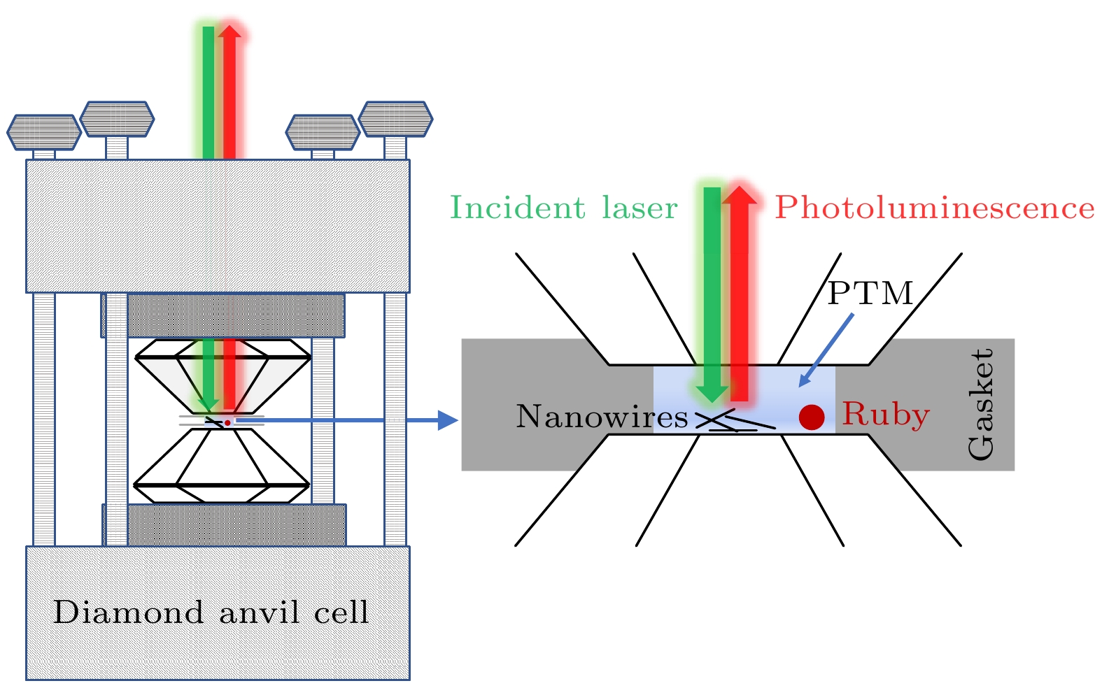
图 1 金刚石对顶砧加压装置以及光学测量时样品腔内示意图
Fig. 1. Schematic diagram of the diamond anvil cell (DAC) and the sample cavity during optical measurements.
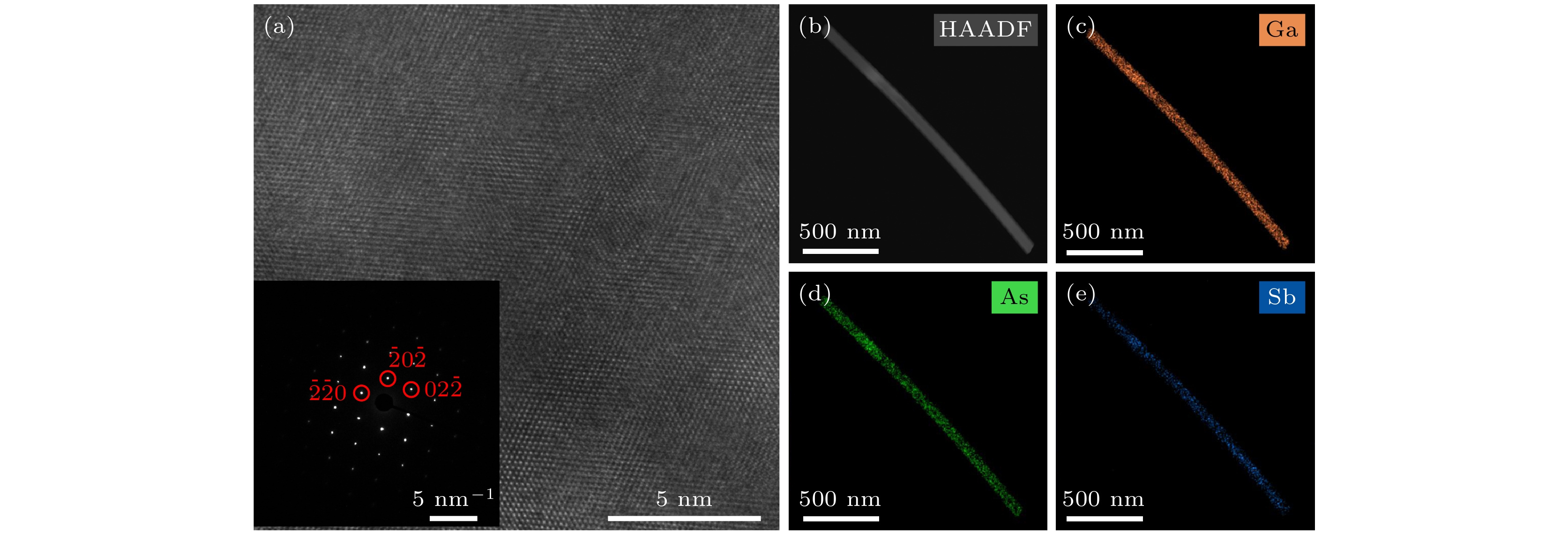
图 2 (a) GaAsSb三元纳米线的高分辨率透射电子显微镜图像, 左下角为其电子衍射图; (b) GaAsSb三元纳米线的高角度环形暗场成像; (c)—(e) GaAsSb三元纳米线中Ga元素、As元素、Sb元素对应的伪彩色EDS映射图
Fig. 2. (a) HRTEM image of GaAsSb nanowires (NWs) with the corresponding electron diffraction pattern image in left bottom; (b) HAADF image of GaAsSb NWs; (c)–(e) false color EDS maps of GaAsSb NWs with the Ga element, As element and Sb element
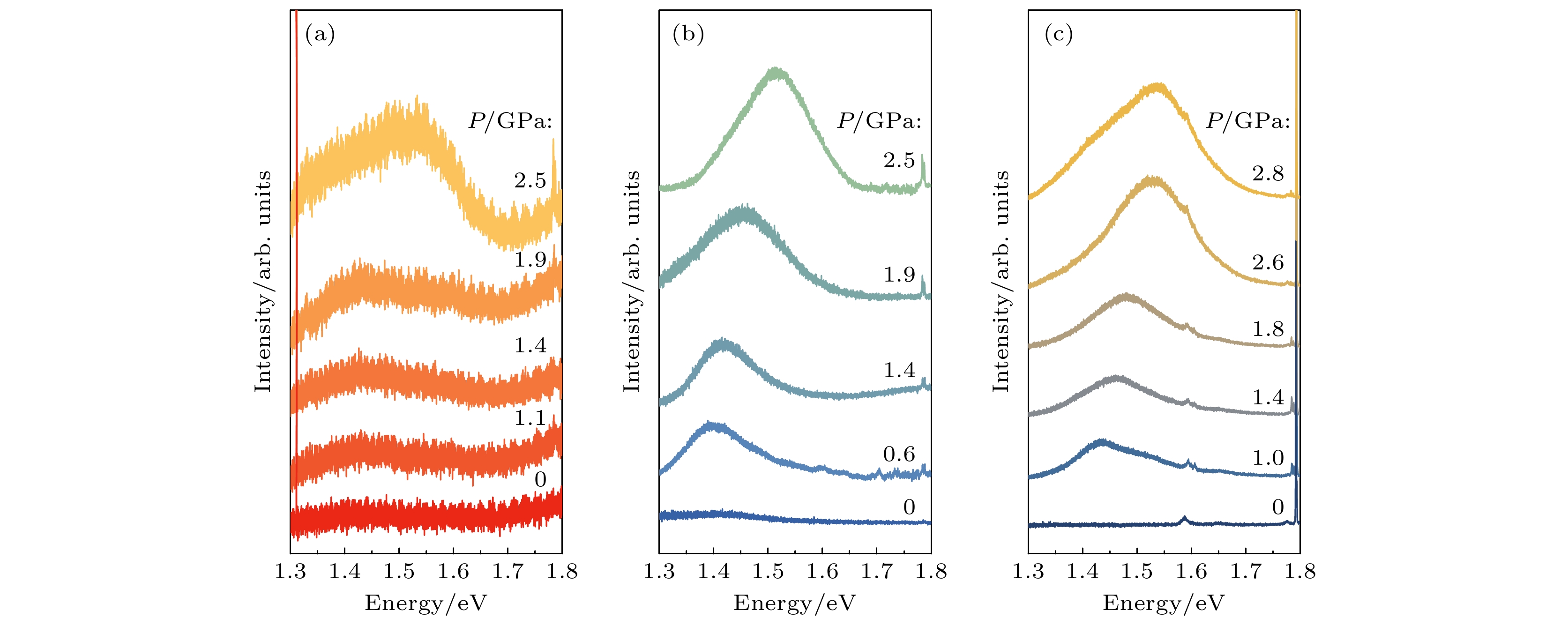
图 3 室温条件下, 在(a) 473 nm, (b) 514 nm和(c) 633 nm三种不同波长激光激发下, GaAsSb纳米线的荧光光谱随压力的变化情况
Fig. 3. Pressure-dependent photoluminescence (PL) spectra of GaAsSb NWs obtained at ambient temperature with the excitation wavelength of (a) 473 nm, (b) 514 nm, and (c) 633 nm.
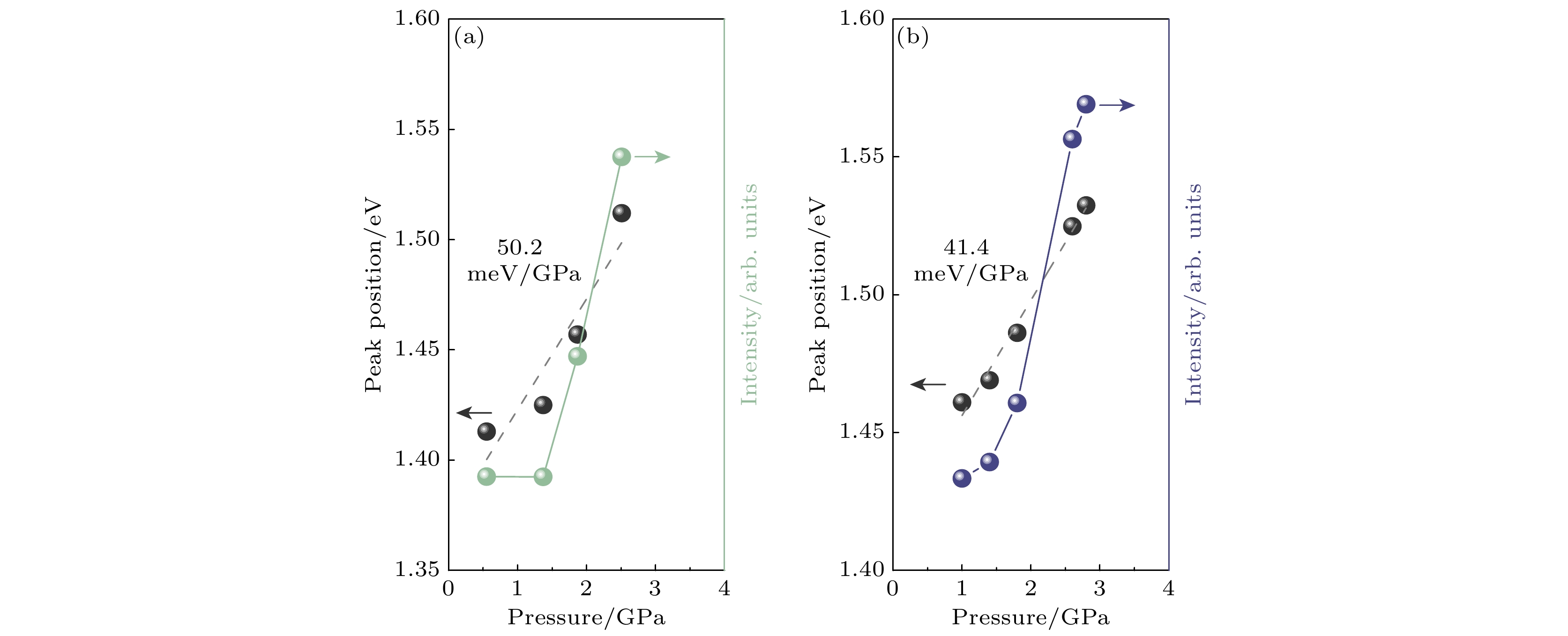
图 4 在(a) 514 nm和(b) 633 nm两种不同波长激光激发下GaASbs纳米线的荧光峰峰位(左边Y轴)和强度(右边Y轴)随压力的变化情况, 其中黑色虚线是荧光峰位与压力的线性拟合结果
Fig. 4. Pressure dependence of the PL emission position (left Y-axis) and intensity (right Y-axis) of GaAsSb nanowires with excitation wavelength of (a) 514 nm, (b) 633 nm. The dashed line represents the linear fit results between the PL emission position and pressure.
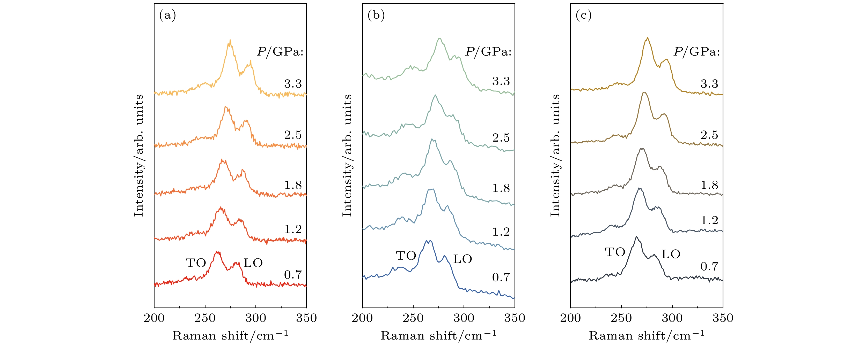
图 5 室温条件下, 在(a) 473 nm, (b) 514 nm和(c) 633 nm三种不同波长激光激发下GaAsSb纳米线的高压拉曼光谱
Fig. 5. High-pressure Raman spectra of GaAsSb NWs at room temperature with excitation wavelength of (a) 473 nm, (b) 514 nm, and (c) 633 nm.
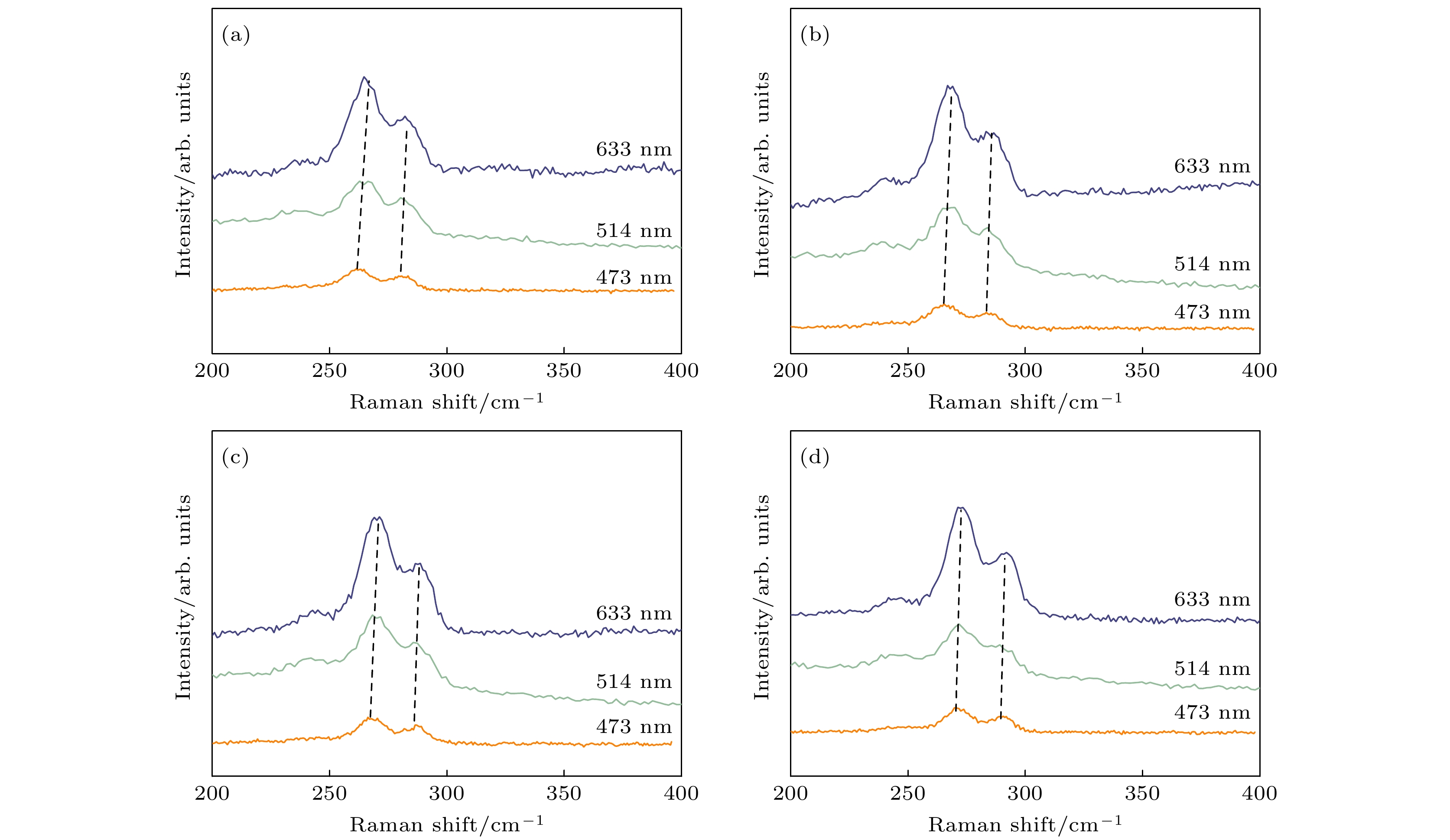
图 6 在(a) 0.7 GPa, (b) 1.2 GPa, (c) 1.8 GPa和(d) 2.5 GPa四个压力点下由473 nm, 514 nm和633 nm 三种不同波长激光激发得到的拉曼峰对比
Fig. 6. Raman spectra stimulated by incident laser at wavelengths of 473 nm, 514 nm, and 633 nm under the pressures of (a) 0.7 GPa, (b) 1.2 GPa, (c) 1.8 GPa, (d) 2.5 GPa.
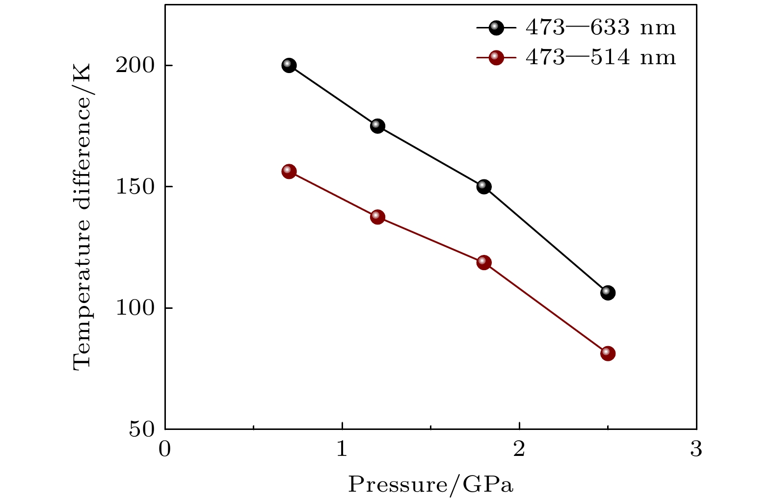
图 7 不同压力下由两种不同波长入射激光引起的相对温差
Fig. 7. Pressure dependence of the relative temperature difference excited by the selected two different incident lasers.
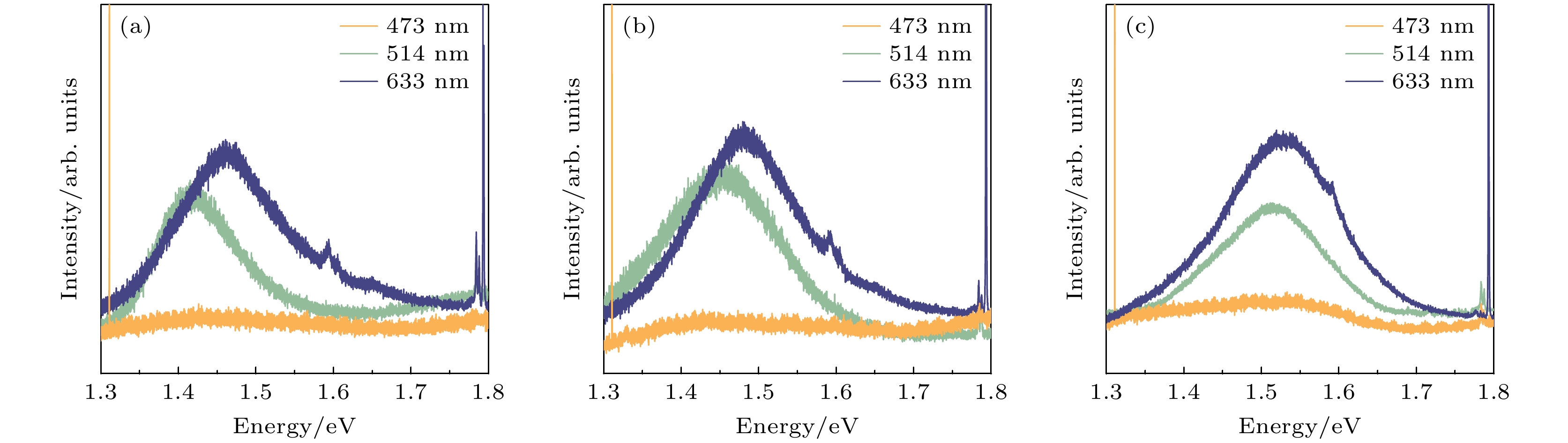
图 8 (a) 1.4 GPa, (b) 1.8 GPa, (c) 2.5 GPa三个压力点下由473 nm, 514 nm和633 nm三种不同波长激光激发得到的荧光峰对比
Fig. 8. The PL spectra stimulated by incident laser at different wavelengths of 473 nm, 514 nm, and 633 nm under the pressure of (a) 1.4 GPa, (b) 1.8 GPa, (c) 2.5 GPa.
表 1 不同压力下由3种波长的激发光激发的拉曼峰的TO模式峰位.
Table 1. The TO mode Raman peak positions stimulated by laser at different wavelengths under different pressures.
TO/cm–1 0.7 GPa 1.2 GPa 1.8 GPa 2.5 GPa 473 nm 261.7 265.0 267.8 271.2 514 nm 264.2 267.2 269.7 272.5 633 nm 264.9 267.8 270.2 272.9  下载: 导出CSV
-
[1] Liu X, Gu L L, Zhang Q P, Wu J Y, Long Y Z, Fan Z Y 2014 Nat. Commun. 5 4007
Google Scholar
[2] Guo W, Zhang M, Banerjee A, Bhattacharya P 2010 Nano Lett. 10 3355
Google Scholar
[3] Cui Y, Wei Q Q, Park H K, Lieber C M 2001 Science 293 1289
Google Scholar
[4] Tian B Z, Zheng X L, Kempa T J, Fang Y, Yu N F, Yu G H, Huang J L, Lieber C M 2007 Nature 449 885
Google Scholar
[5] Nowzari A, Heurlin M, Jain V, Storm K, Hosseinnia A, Anttu N, Borgström M T, Pettersson H, Samuelson L 2015 Nano Lett. 15 1809
Google Scholar
[6] Zhang Q, Ha S T, Liu X F, Sum T C, Xiong Q H 2014 Nano Lett. 14 5995
Google Scholar
[7] Duan X F, Huang Y, Agarwal R, Lieber C M 2003 Nature 421 241
Google Scholar
[8] Dai X, Zhang S, Wang Z L, Adamo G, Liu H, Huang Y Z, Couteau C, Soci C 2014 Nano Lett. 14 2688
Google Scholar
[9] Soci C, Zhang A, Bao X Y, Kim H, Lo Y, Wang D 2010 J. Nanosci. Nanotechno. 10 1430
Google Scholar
[10] Dick K A 2008 Prog. Cryst. Growth Ch. 54 138
Google Scholar
[11] Zhang L L, Li X, Cheng S B, Shan C X 2022 Materials 15 1917
Google Scholar
[12] Duan X, Wang J, Lieber C M 2000 Appl. Phys. Lett. 76 1116
Google Scholar
[13] Li L X, Pan D, Xue Y Z, Wang X L, Lin M L 2017 Nano Lett. 17 622
Google Scholar
[14] Li Z Y, Yuan X M, Gao Q, Yang I, Li L, Caroff P, Allen M, Allen J, Tan H H, Jagadish C, Fu L 2020 Nanotechnology 31 244002
Google Scholar
[15] Wang W, Yip S P, Meng Y, Wang W J, Wang F, Bu X M, Lai Z X, Kang X L, Xie P S, Quan Q, Liu C T, Ho J C 2021 Adv. Opt. Mater. 9 22
Google Scholar
[16] Zhuo R, Wen L J, Wang J, Dou X M, Liu L, Hou X Y, Liao D Y, Sun B Q, Pan D, Zhao J H 2024 Sci. China Phys. Mech. 67 127311
Google Scholar
[17] Chandrasekhar M, Pollak F H 1977 Phys. Rev. B 15 2127
Google Scholar
[18] Liang Y L, Yao Z, Yin X T, Wang P, Li L X, Pan D, Li H Y, Li Q J, Liu B B, Zhao J H 2019 Chin. Phys. B 28 076401
Google Scholar
[19] Zhou W, Chen X J, Zhang J B, Li X H, Wang Y Q, Goncharov A F 2014 Sci. Rep 4 6472
Google Scholar
[20] Yin X T, Liang Y L, Li L X, Liu S, Pan D, Wang P 2024 Nanotechnology 35 245702
Google Scholar
[21] Yazji S, Zardo I, Soini M, Postorino P, Morral A F I, Abstreiter G 2011 Nanotechnology 22 325701
Google Scholar
[22] Majumdar D, Ercolani D, Sorba L, Singha A 2016 J. Mater. Chem. C 4 2339
Google Scholar
[23] Zardo I, Yazji S, Marini C, Uccelli E, Morral A F I, Abstreiter G, Postorino P 2012 ACS Nano 6 3284
Google Scholar
[24] Ma L M, Wang P, Yin X T, Liang Y L, Liu S, Li L X, Pan D, Yao Z, Liu B B, Zhao J H 2020 Nanoscale Adv. 2 2558
Google Scholar
[25] Chang C C, Chi C Y, Yao M Q, Huang N F, Chen C C, Theiss J, Bushmaker A W, LaLumondiere S, Yeh T W, Povinelli M L, Zhou C W, Dapkus P D, Cronin S B 2012 Nano Lett. 12 4484
Google Scholar
[26] Soini M, Zardo I, Uccelli E, Funk S, Koblmuller G, Morral A F I, Abstreiter G 2010 Appl. Phys. Lett. 97 263107
Google Scholar


 下载:
下载:


计量
- 文章访问数: 2299
- PDF下载量: 113
- 被引次数: 0
