


-
Due to the outstanding mechanical and electronic properties, graphene has been widely investigated as the nano-filler for fabricating metallic matrix composites. The key point in these studies is how to realize a uniform distribution of graphene in the metallic powders. The traditional methods mainly include ball-milling and colloidal processing. However, both of them result in massive structural defects on graphene flakes and further degrade its strengthening effects. Therefore, it is meaningful to explore a new method. In this study, we present a new way, i.e. in-situ growth of graphene on copper powders in the plasma enhanced chemical vapor deposition system (PECVD). The scanning electron microscope(SEM) images indicate that the powder is fully covered by graphene nanoflakes, realizing uniform mixing on a micro-scale. Further research finds that there exists a competition between growth and etching at the initial stage of the graphene growth. Methane is dissociated into various active species (CHx, atomic H and C) by the radio frequency. The C atoms self-assemble into graphene islands, yet the H atoms tend to etch these islands away. At a lower temperature, the etching effect takes a dominant position and then only the bigger islands are able to survive in this process, resulting in bigger graphene nanoflakes. As a contrast, it is a growth-dominant process at higher temperature, resulting in a much higher nucleation density and smaller graphene sheets. Therefore, the size of graphene sheets can be well controlled by tuning the growth temperature, for example, the sizes are 300 and 100 nm at 500 ℃ and 600 ℃ respectively. Moreover, the X-ray photoelectron spectroscopy(XPS) spectra show that the oxide layer at the surface of copper powder can be removed as the graphene flakes grow, which contributes to a fine interface between the two parts and further leads to outstanding performance of the final composite. The powder is consolidated by spark plasma sintering(SPS) technique, and several properties of this composite are tested. The results indicate that compared with the pure copper, the copper with the addition of graphene can reduce the resistivity by one order of magnitude and increase the hardness and yield strength by 15.6% and 28.8%, respectively. This work provides an alternative way to fabricate graphene-enforced composite and shows promising application prospects.
-
Keywords:
- composite /
- copper powder /
- graphene /
- chemical vapor deposition
[1] Hwang J, Yoon T, Jin S H, Lee J, Kim T S, Hong S H, Jeon S 2013 Adv. Mater. 25 6724
 Google Scholar
[2] Li Z, Guo Q, Li Z Q, Fan G L, Xiong D B, Su Y S, Zhang J, Zhang D 2015 Nano Lett. 15 8077
Google Scholar
[3] Yue H Y, Yao L H, Gao X, Zhang S L, Guo E J, Zhang H, Lin X Y, Wang B 2017 J. Alloys Compd. 691 755
Google Scholar
[4] Li J F, Zhang L, Xiao J K, Zhou K C 2015 Trans. Nonferrous Met. Soc. China 25 3354
Google Scholar
[5] 燕绍九, 杨程, 洪起虎, 陈军洲, 刘大博, 戴圣龙 2014 材料工程 0(4) 1
Google Scholar
Yan S J, Yang C, Hong Q H, Chen J Z, Liu D B, Dai S L 2014 J. Mater. Eng. 0(4) 1
Google Scholar
[6] Kim Y, Lee J, Yeom M S, Shin J W, Kim H, Cui Y, Kysar J W, Hone J, Jung Y, Jeon S, Han S M 2013 Nat. Commun. 4 2114
Google Scholar
[7] Liu J, Yan H X, Jiang K 2013 Ceram. Int. 39 6215
Google Scholar
[8] Pavithra C L P, Sarada B V, Rajulapati K V, Rao T N, Sundararajan G 2014 Sci. Rep. 4 4049
[9] Porwal H, Tatarko P, Grasso S, Khaliq J, Dlouhy I, Reece M J 2013 Carbon 64 359
Google Scholar
[10] Wang J Y, Li Z Q, Fan G L, Pan H H, Chen Z X, Zhang D 2012 Scr. Mater. 66 594
Google Scholar
[11] Nieto A, Huang L, Han Y H, Schoenung J M 2015 Ceram. Int. 41 5926
Google Scholar
[12] Ramirez C, Osendi M I 2014 Ceram. Int. 40 11187
Google Scholar
[13] Gutierrez-Gonzalez C F, Smirnov A, Centeno A, Fernandez A, Alonso B, Rocha V G, Torrecillas R, Zurutuza A, Bartolome J F 2015 Ceram. Int. 41 7434
Google Scholar
[14] Poirier D, Gauvin R, Drew R A L 2009 Composites Part A 40 1482
Google Scholar
[15] Li Z, Fan G L, Tan Z Q, Guo Q, Xiong D B, Su Y S, Li Z Q, Zhang D 2014 Nanotechnology 25 325601
Google Scholar
[16] Jiang L L, Yang T Z, Liu F, Dong J, Yao Z H, Shen C M, Deng S Z, Xu N S, Liu Y Q, Gao H J 2013 Adv. Mater. 25 250
Google Scholar
[17] Graf D, Molitor F, Ensslin K, Stampfer C, Jungen A, Hierold C, Wirtz L 2007 Nano Lett. 7 238
Google Scholar
[18] Zhou H T, Yu N, Zou F, Yao Z H, Gao G, Shen C M 2016 Chin. Phys. B 25 096106
Google Scholar
[19] Zhou H T, Liu D B, Luo F, Tian Y, Chen D S, Luo B W, Zhou Z, Shen C M 2019 Chin. Phys. B 28 068102
Google Scholar
[20] Liu D H, Yang W, Zhang L C, Zhang J, Meng J L, Yang R, Zhang G Y, Shi D X 2014 Carbon 72 387
Google Scholar
[21] Zhang L C, Shi Z W, Liu D H, Yang R, Shi D X, Zhang G Y 2012 Nano Res. 5 258
Google Scholar
[22] Liu Z J, Zhao Z H, Wang Y Y, Dou S, Yan D F, Liu D D, Xia Z H, Wang S Y 2017 Adv. Mater. 29 1606207
Google Scholar
[23] 李秀辉, 燕绍九, 洪起虎, 赵双赞, 陈翔 2019 材料工程 47(1) 11
Google Scholar
Li X H, Yan S J, Hong Q H, Zhao S Z, Chen X 2019 J. Mater. Eng. 47(1) 11
Google Scholar
[24] Bartoluccia S, Parasa J, Rafieeb M, Rafieec J, Leea S, Kapoora D, Koratkarc N 2011 Mater. Sci. Eng., A 528 7933
Google Scholar
[25] Chen D S, Zhou H T, Tian Y, Luo F, Liu D B, Luo B W 2019 Micro-Nano Lett. 14 613
Google Scholar
-
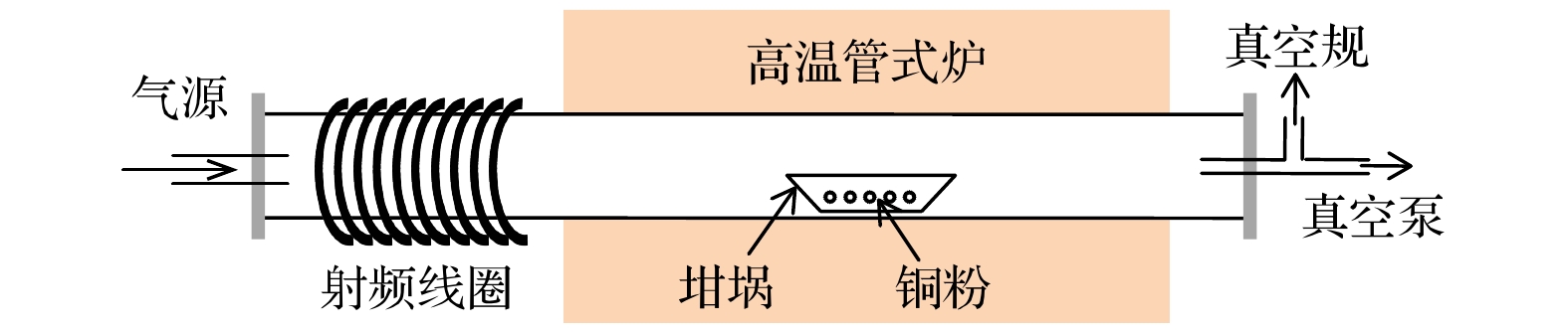
图 1 等离子增强化学气相沉积系统示意图
Figure 1. Schematic presentation of plasma enhanced chemical vapor deposition system (PECVD).

图 2 利用等离子增强化学气相沉积方法在铜粉表面制备竖直站立石墨烯 (a)前和(b)后的SEM图; (c) 拉曼光谱; (d) 石墨烯边缘的HR-TEM图; 不同温度下制备的石墨烯的SEM图((e) 600 ℃和(f) 500 ℃, 生长时间为20和40 min), 结果表明可以通过调节生长温度, 控制石墨烯纳米片的尺寸
Figure 2. The SEM image of the copper powder (a) before and (b) after the deposition of graphene; (c) Raman spectra of graphene; (d) HR-TEM image of the edge of graphene; the SEM image of graphene deposited at different temperatures ((e) 600 ℃ and (f) 500 ℃), indicating the size of graphene can be well controlled by tuning the growth temperature.

图 3 (a) 铜原子的电子排布示意图; (b) XPS全谱扫描谱线; (c) C 1s精细谱; (d) Cu 2p精细谱
Figure 3. (a) The electron configuration of copper atom; (b) XPS of the graphene grown on copper powder; (c) C 1s spectra; (d) Cu 2p spectra.
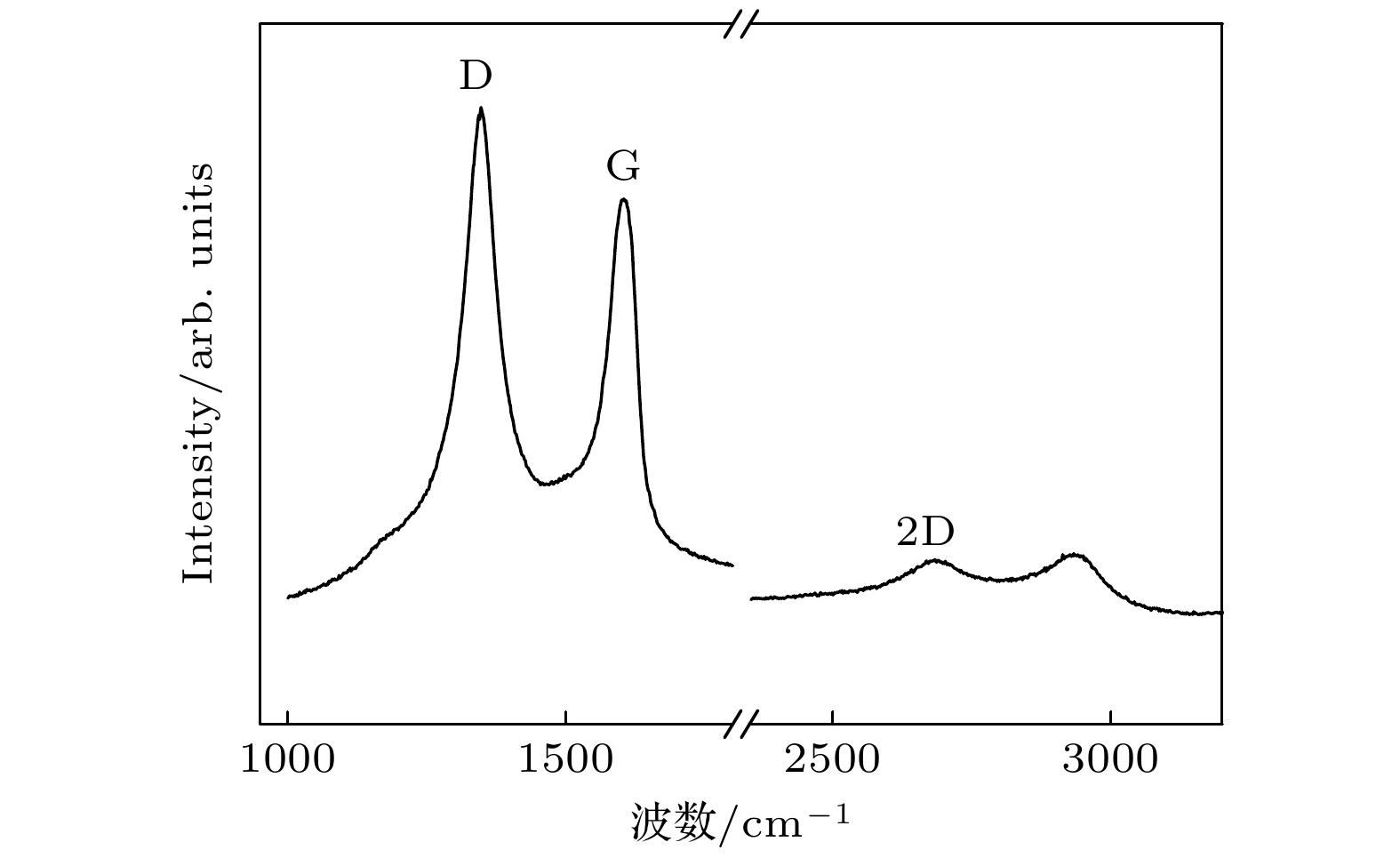
图 4 添加石墨烯铜粉经SPS成型后样品的拉曼光谱曲线
Figure 4. Raman spectroscopy of the graphene-added copper alloy, prepared by spark plasma sinter of the graphene-copper powders.
表 1 放电等离子烧结样品的性能表征结果
Table 1. The properties of the spark plasma sintered samples.
密度/
(g·cm–3)电阻率/
(10–5 Ω·cm)维氏硬
度/HV屈服强
度/MPa未添加石墨烯样品 8.74 24.60 77 52 添加石墨烯样品 8.37 1.36 89 67  DownLoad: CSV
-
[1] Hwang J, Yoon T, Jin S H, Lee J, Kim T S, Hong S H, Jeon S 2013 Adv. Mater. 25 6724
Google Scholar
[2] Li Z, Guo Q, Li Z Q, Fan G L, Xiong D B, Su Y S, Zhang J, Zhang D 2015 Nano Lett. 15 8077
Google Scholar
[3] Yue H Y, Yao L H, Gao X, Zhang S L, Guo E J, Zhang H, Lin X Y, Wang B 2017 J. Alloys Compd. 691 755
Google Scholar
[4] Li J F, Zhang L, Xiao J K, Zhou K C 2015 Trans. Nonferrous Met. Soc. China 25 3354
Google Scholar
[5] 燕绍九, 杨程, 洪起虎, 陈军洲, 刘大博, 戴圣龙 2014 材料工程 0(4) 1
Google Scholar
Yan S J, Yang C, Hong Q H, Chen J Z, Liu D B, Dai S L 2014 J. Mater. Eng. 0(4) 1
Google Scholar
[6] Kim Y, Lee J, Yeom M S, Shin J W, Kim H, Cui Y, Kysar J W, Hone J, Jung Y, Jeon S, Han S M 2013 Nat. Commun. 4 2114
Google Scholar
[7] Liu J, Yan H X, Jiang K 2013 Ceram. Int. 39 6215
Google Scholar
[8] Pavithra C L P, Sarada B V, Rajulapati K V, Rao T N, Sundararajan G 2014 Sci. Rep. 4 4049
[9] Porwal H, Tatarko P, Grasso S, Khaliq J, Dlouhy I, Reece M J 2013 Carbon 64 359
Google Scholar
[10] Wang J Y, Li Z Q, Fan G L, Pan H H, Chen Z X, Zhang D 2012 Scr. Mater. 66 594
Google Scholar
[11] Nieto A, Huang L, Han Y H, Schoenung J M 2015 Ceram. Int. 41 5926
Google Scholar
[12] Ramirez C, Osendi M I 2014 Ceram. Int. 40 11187
Google Scholar
[13] Gutierrez-Gonzalez C F, Smirnov A, Centeno A, Fernandez A, Alonso B, Rocha V G, Torrecillas R, Zurutuza A, Bartolome J F 2015 Ceram. Int. 41 7434
Google Scholar
[14] Poirier D, Gauvin R, Drew R A L 2009 Composites Part A 40 1482
Google Scholar
[15] Li Z, Fan G L, Tan Z Q, Guo Q, Xiong D B, Su Y S, Li Z Q, Zhang D 2014 Nanotechnology 25 325601
Google Scholar
[16] Jiang L L, Yang T Z, Liu F, Dong J, Yao Z H, Shen C M, Deng S Z, Xu N S, Liu Y Q, Gao H J 2013 Adv. Mater. 25 250
Google Scholar
[17] Graf D, Molitor F, Ensslin K, Stampfer C, Jungen A, Hierold C, Wirtz L 2007 Nano Lett. 7 238
Google Scholar
[18] Zhou H T, Yu N, Zou F, Yao Z H, Gao G, Shen C M 2016 Chin. Phys. B 25 096106
Google Scholar
[19] Zhou H T, Liu D B, Luo F, Tian Y, Chen D S, Luo B W, Zhou Z, Shen C M 2019 Chin. Phys. B 28 068102
Google Scholar
[20] Liu D H, Yang W, Zhang L C, Zhang J, Meng J L, Yang R, Zhang G Y, Shi D X 2014 Carbon 72 387
Google Scholar
[21] Zhang L C, Shi Z W, Liu D H, Yang R, Shi D X, Zhang G Y 2012 Nano Res. 5 258
Google Scholar
[22] Liu Z J, Zhao Z H, Wang Y Y, Dou S, Yan D F, Liu D D, Xia Z H, Wang S Y 2017 Adv. Mater. 29 1606207
Google Scholar
[23] 李秀辉, 燕绍九, 洪起虎, 赵双赞, 陈翔 2019 材料工程 47(1) 11
Google Scholar
Li X H, Yan S J, Hong Q H, Zhao S Z, Chen X 2019 J. Mater. Eng. 47(1) 11
Google Scholar
[24] Bartoluccia S, Parasa J, Rafieeb M, Rafieec J, Leea S, Kapoora D, Koratkarc N 2011 Mater. Sci. Eng., A 528 7933
Google Scholar
[25] Chen D S, Zhou H T, Tian Y, Luo F, Liu D B, Luo B W 2019 Micro-Nano Lett. 14 613
Google Scholar


 DownLoad:


Catalog
Metrics
- Abstract views: 11440
- PDF Downloads: 222
- Cited By: 0
