


-
Two-dimensional (2D) hexagonal boron nitride (hBN) possesses many unique properties such as high mechanical strength and excellent chemical and thermal stability. The 2D hBN exhibits a wide bandgap in the UV region and optically-stable ultra-bright quantum emitters that make hBN a promising nanophotonic platform for quantum computing and information processing, especially in the visible wavelength range. Therefore, it is greatly important to build up different nanophotonic devices with different functionalities based on this material platform to achieve the integrated photonic chips. Among the devices, the integratable optical asymmetric transmission devices are important elements for functional quantum computing chips. Since hBN is a dielectric material, photonic crystal (PhC) structure is the most suitable in principle and allows on-chip integration with other photonic devices. In this study, we theoretically design an asymmetric transmission device based on 2D hBN PhC heterostructures in the visible wavelength range for the first time. Due to the relatively low refractive index of 2D hBN material (n < 2.4), we design a free-standing hBN PhC heterostructure to maximize the light trapping in the structure and minimize the propagation loss. The asymmetric transmission device is composed of two square-lattice 2D PhC structures, namely PhC 1 and PhC 2. We use the plane wave expansion method (PWM) to calculate the iso-frequency contours (EFCs) of the PhC structures to study the light propagation inside of the PhCs, which will propagate along the gradient of direction of the EFCs. We design the PhC structure in the way that the incident light beams from different angles can be self-collimated along the Г-X direction of the PhC 2 and coupled out. On the other hand, the backward incident light is blocked by the bandgaps of PhC 2. In this way, asymmetric optical transmission is achieved with high forward transmittance and contrast ratio. In addition, we further finely tune the structural parameters, including the lattice constant and column radius of the PhCs to optimize the performance by using the finite difference time domain (FDTD) method. The resulting 2D hBN PhC heterostructure achieves an asymmetric transmission in a wavelength range of 610–684 nm with a peak forward transmittance of 0.65 at a wavelength of 652 nm. Meanwhile, the backward transmittance is controlled to be 0.04. As a result, the contrast ratio can reach up to 0.95. The working bandwidth of the hBN PhC is 74 nm (TF > 0.5). In addition, the designed asymmetric transmission device has a small size of 11 μm × 11 μm, thus it is suitable for on-chip integration. Our results open up possibilities for designing new nanophotonic devices based on 2D hBN material for quantum computing and information processing. The design principle can be generally used to design other photonic devices based on 2D hBN material.
-
Keywords:
- asymmetric transmission /
- two-dimensional hexagonal boron nitride /
- photonic crystal /
- heterostructure
[1] Xu M, Liang T, Shi M, Chen H 2013 Chem. Rev. 113 3766
 Google Scholar
[2] Novoselov K S, Geim A K, Morozov S V, Jiang D, Katsnelson M I, Grigorieva I V, Dubonos S V, Firsov A A 2005 Nature 438 197
Google Scholar
[3] Kubota Y, Watanabe K, Tsuda O, Taniguchi T 2007 Science 317 932
Google Scholar
[4] Song L, Ci L, Lu H, Sorokin P B, Jin C, Ni J, Kvashnin A G, Kvashnin D G, Lou J, Yakobson B I, Ajayan P M 2010 Nano Lett. 10 3209
Google Scholar
[5] Nersisyan H H, Lee T H, Lee K H, An Y S, Lee J S, Lee J H 2015 RSC Adv. 5 8579
Google Scholar
[6] Glavin N R, Jespersen M L, Check M H, Hu J, Hilton A M, Fisher T S, Voevodin A A 2014 Thin Solid Films 572 245
Google Scholar
[7] Zhi C, Bando Y, Tang C, Kuwahara H, Golberg D 2009 Adv. Mater. 21 2889
Google Scholar
[8] Doan T C, Majety S, Grenadier S, Li J, Lin J Y, Jiang H X 2015 Nucl. Instrum. Methods 783 121
Google Scholar
[9] Barboza A P M, Chacham H, Oliveira C K, Fernandes T F D, Ferreira E H M, Archanjo B S, Batista R J C, De Oliveira A B, Neves B R A 2012 Nano Lett. 12 2313
Google Scholar
[10] Barcelos I D, Cadore A R, Campos L C, Malachias A, Watanabe K, Taniguchi T, Maia F C, Freitas R, Deneke C 2015 Nanoscale 7 11620
Google Scholar
[11] Watanabe K, Taniguchi T, Kanda H 2004 Nat. Mater. 3 404
Google Scholar
[12] Nebel C E 2009 Nat. Photonics 3 564
Google Scholar
[13] Shotan Z, Jayakumar H, Considine C R, Mackoit M, Fedder H, Wrachtrup J R, Alkauskas A, Doherty M W, Menon V M, Meriles C A 2016 ACS Photonics 3 2490
Google Scholar
[14] Chejanovsky N, Rezai M, Paolucci F, Kim Y, Rendler T, Rouabeh W, Fávaro d O F, Herlinger P, Denisenko A, Yang S 2016 Nano Lett. 16 7037
Google Scholar
[15] Bourrellier R, Meuret S, Tararan A, Stã©Phan O, Kociak M, Tizei L H, Zobelli A 2016 Nano Lett. 16 4317
Google Scholar
[16] Kim S, Fröch J E, Christian J, Straw M, Bishop J, Totonjian D, Watanabe K, Taniguchi T, Toth M, Aharonovich I 2018 Nat. Commun. 9 2623
Google Scholar
[17] Jalas D, Petrov A, Eich M, Freude W, Fan S, Yu Z, Baets R, Popović M, Melloni A, Joannopoulos J D 2013 Nat. Photonics 7 579
Google Scholar
[18] Qiang X, Zhou X, Wang J, Wilkes C M, Loke T, O’Gara S, Kling L, Marshall G D, Santagati R, Ralph T C 2018 Nat. Photonics 12 534
Google Scholar
[19] Fei H M, Wu J J, Yang Y B, Liu X, Chen Z H 2015 Photonics Nanostruct. 17 15
Google Scholar
[20] Yu G X, Fu J J, Du W W, Lu Y H, Luo M 2019 Chin. Phys. B 28 024101
Google Scholar
[21] Liu D Y, Yao L F, Zhai X M, Li M H, Dong J F 2014 Appl. Phys. A 116 9
Google Scholar
[22] Feng S, Wang Y Q 2013 Opt. Express 21 220
Google Scholar
[23] Kim M, Yao K, Yoon G, Kim I, Liu Y, Rho J 2017 Adv. Opt. Mater. 5 1700600
Google Scholar
[24] Wang C, Zhou C, Li Z Y 2011 Opt. Express 19 26948
Google Scholar
[25] Fei H M, Wu M, Lin H, Liu X, Yang Y B, Zhang M D, Cao B Z 2019 Superlattices Microstruct. 132 106155
Google Scholar
[26] 费宏明, 徐婷, 刘欣, 林瀚, 陈智辉, 杨毅彪, 张明达, 曹斌照, 梁九卿 2017 66 204103
Google Scholar
Fei H M, Xu T, Liu X, Lin H, Chen Z H, Yang Y B, Zhang M D, Cao B Z, Liang J Q 2017 Acta Phys. Sin. 66 204103
Google Scholar
[27] Li J, Ye H, Yu Z, Liu Y 2017 Opt. Express 25 19129
Google Scholar
[28] Fei H M, Zhang Q, Wu M, Lin H, Liu X, Yang Y B, Zhang M D, Guo R, Han X T 2020 Appl. Opt. 59 4416
Google Scholar
[29] Kim J, Lee S Y, Park H, Lee K, Lee B 2015 Opt. Express 23 9004
Google Scholar
[30] Gao H, Zheng Z, Dong J, Feng J, Zhou J 2015 Opt. Commun. 355 137
Google Scholar
[31] Wang C, Zhong X L, Li Z Y 2012 Sci. Rep. 2 674
Google Scholar
[32] Kim S, Toth M, Aharonovich I 2018 Beilstein J. Nanotechnol. 9 102
Google Scholar
[33] Plihal M, Maradudin A A 1991 Phys. Rev. B 44 8565
Google Scholar
[34] Feng S, Wang Y Q 2013 Opt. Mater. 36 546
Google Scholar
[35] Chan C T, Yu Q L, Ho K M 1995 Phys. Rev. B 51 16635
Google Scholar
-
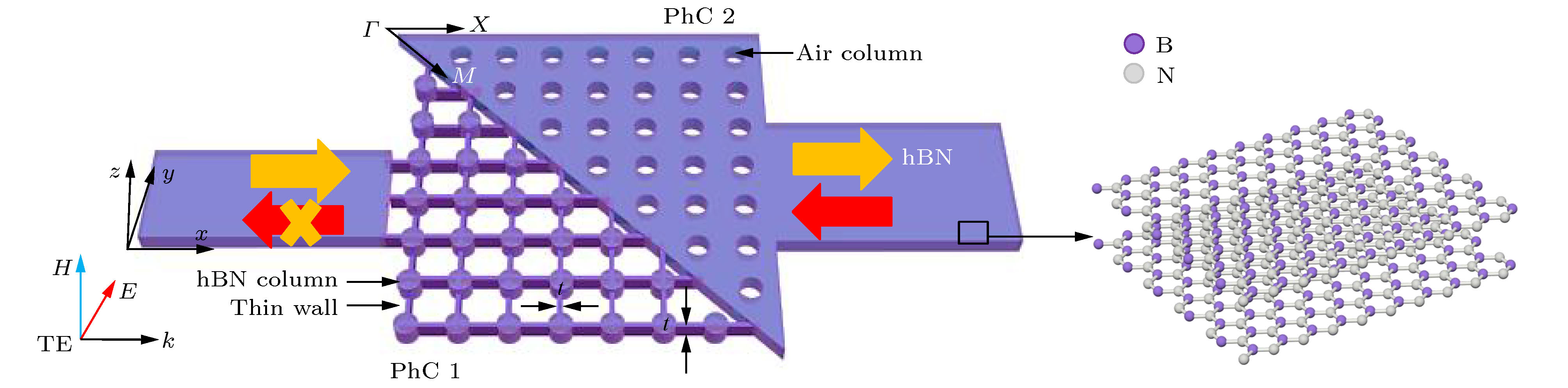
图 1 基于二维hBN PhC异质结构的光波非对称传输示意图, 右图为二维hBN材料的分子结构图
Figure 1. Schematic diagram of the two-dimensional hBN PhC heterostructure for asymmetric transmission of light. The right picture is the molecular structure of two-dimensional hBN material.

图 2 (a) PhC 1的能带图; (b) PhC 2的能带图, 阴影部分代表Γ-X方向禁止光波传输的频带
Figure 2. (a) The band diagrams of the PhC 1; (b) the band diagrams of the PhC 2. The shaded area represents the frequency band in which light transmission is prohibited at the Γ-X direction.
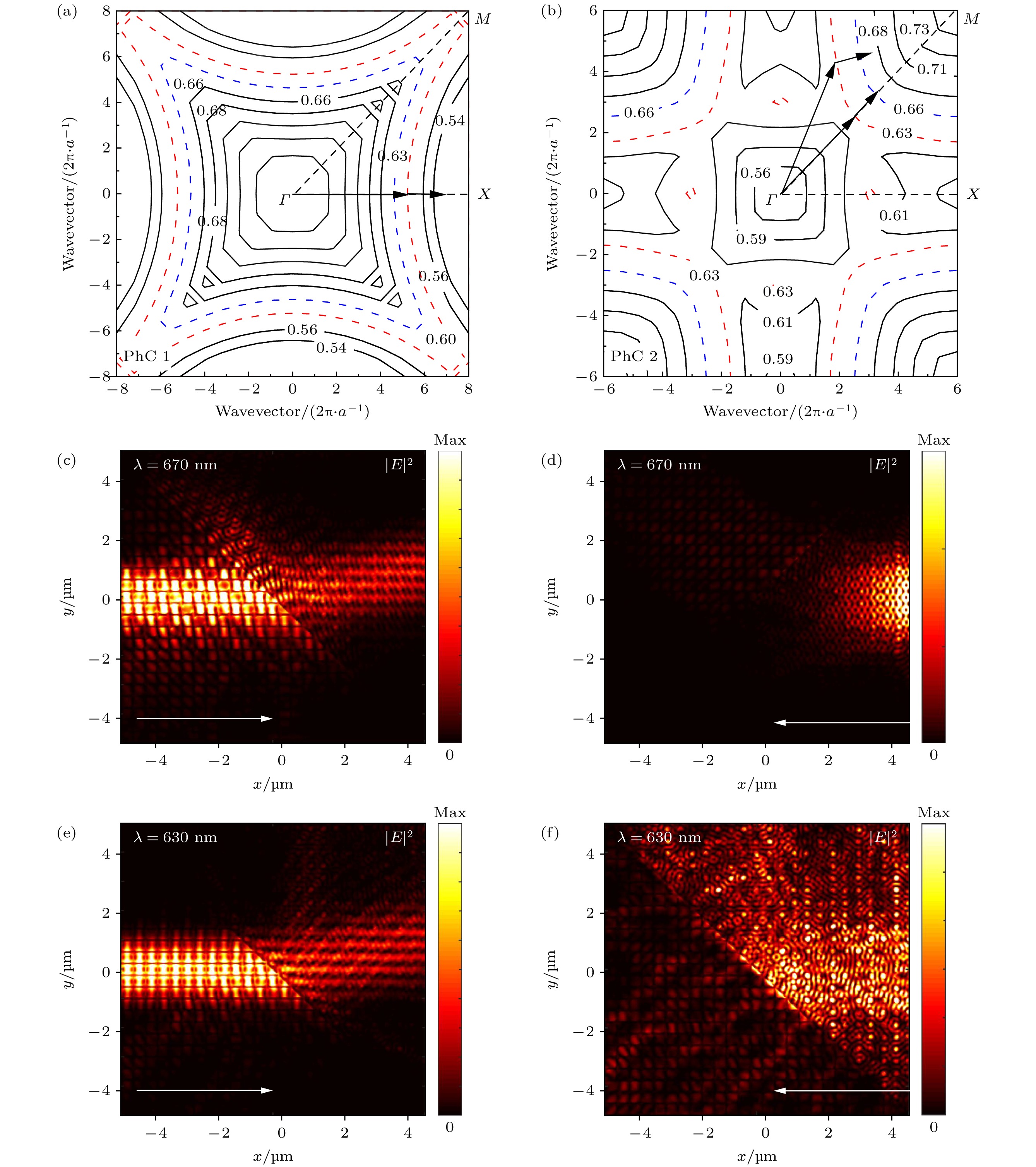
图 3 (a) PhC 1中TE偏振模式下第二条能带对应的等频图; (b) PhC 2中TE偏振模式下第五条能带对应的等频图(红色和蓝色虚线表示670和630 nm对应的等频线). TE偏振的正向入射光 (c) 和反向入射光 (d) 在670 nm波长处的电场强度分布图; 正向入射光(e)和反向入射光(f)在630 nm波长处的电场强度分布图
Figure 3. (a) The EFCs of the second band in PhC 1 for TE polarization; (b) the EFCs of the fifth band in PhC 2 for TE polarization (The red and blue dotted lines represent the EFCs corresponding to 670 and 630 nm). The electric field intensity distribution diagrams of forward incident light (c) and backward incident light (d) of TE polarization at the wavelength of 670 nm. The electric field intensity distribution diagrams of forward incident light (e) and backward incident light (f) of TE polarization at the wavelength of 630 nm

图 4 PhC 1取不同晶格常数 (a) 与不同柱子半径(b) 的透射率; 异质结构中PhC 2取不同的晶格常数(c) 与柱子半径(d) 的透射率
Figure 4. The transmittance spectra of PhC 1 on the different lattice constants of PhC 1 (a) and the different radii of the columns (b). The transmittance spectra of the heterostructure on the different lattice constants of PhC 2 (c) and the different radii of the columns (d).

图 5 (a) 二维hBN PhC异质结构的透射光谱图; (b) 有限厚度为2000 nm时, 二维hBN PhC平板异质结构的透射光谱图
Figure 5. The transmittance spectra of the two dimensional hBN photonic crystal heterostructure (a) and a slab with thickness of 2000 nm (b).
-
[1] Xu M, Liang T, Shi M, Chen H 2013 Chem. Rev. 113 3766
Google Scholar
[2] Novoselov K S, Geim A K, Morozov S V, Jiang D, Katsnelson M I, Grigorieva I V, Dubonos S V, Firsov A A 2005 Nature 438 197
Google Scholar
[3] Kubota Y, Watanabe K, Tsuda O, Taniguchi T 2007 Science 317 932
Google Scholar
[4] Song L, Ci L, Lu H, Sorokin P B, Jin C, Ni J, Kvashnin A G, Kvashnin D G, Lou J, Yakobson B I, Ajayan P M 2010 Nano Lett. 10 3209
Google Scholar
[5] Nersisyan H H, Lee T H, Lee K H, An Y S, Lee J S, Lee J H 2015 RSC Adv. 5 8579
Google Scholar
[6] Glavin N R, Jespersen M L, Check M H, Hu J, Hilton A M, Fisher T S, Voevodin A A 2014 Thin Solid Films 572 245
Google Scholar
[7] Zhi C, Bando Y, Tang C, Kuwahara H, Golberg D 2009 Adv. Mater. 21 2889
Google Scholar
[8] Doan T C, Majety S, Grenadier S, Li J, Lin J Y, Jiang H X 2015 Nucl. Instrum. Methods 783 121
Google Scholar
[9] Barboza A P M, Chacham H, Oliveira C K, Fernandes T F D, Ferreira E H M, Archanjo B S, Batista R J C, De Oliveira A B, Neves B R A 2012 Nano Lett. 12 2313
Google Scholar
[10] Barcelos I D, Cadore A R, Campos L C, Malachias A, Watanabe K, Taniguchi T, Maia F C, Freitas R, Deneke C 2015 Nanoscale 7 11620
Google Scholar
[11] Watanabe K, Taniguchi T, Kanda H 2004 Nat. Mater. 3 404
Google Scholar
[12] Nebel C E 2009 Nat. Photonics 3 564
Google Scholar
[13] Shotan Z, Jayakumar H, Considine C R, Mackoit M, Fedder H, Wrachtrup J R, Alkauskas A, Doherty M W, Menon V M, Meriles C A 2016 ACS Photonics 3 2490
Google Scholar
[14] Chejanovsky N, Rezai M, Paolucci F, Kim Y, Rendler T, Rouabeh W, Fávaro d O F, Herlinger P, Denisenko A, Yang S 2016 Nano Lett. 16 7037
Google Scholar
[15] Bourrellier R, Meuret S, Tararan A, Stã©Phan O, Kociak M, Tizei L H, Zobelli A 2016 Nano Lett. 16 4317
Google Scholar
[16] Kim S, Fröch J E, Christian J, Straw M, Bishop J, Totonjian D, Watanabe K, Taniguchi T, Toth M, Aharonovich I 2018 Nat. Commun. 9 2623
Google Scholar
[17] Jalas D, Petrov A, Eich M, Freude W, Fan S, Yu Z, Baets R, Popović M, Melloni A, Joannopoulos J D 2013 Nat. Photonics 7 579
Google Scholar
[18] Qiang X, Zhou X, Wang J, Wilkes C M, Loke T, O’Gara S, Kling L, Marshall G D, Santagati R, Ralph T C 2018 Nat. Photonics 12 534
Google Scholar
[19] Fei H M, Wu J J, Yang Y B, Liu X, Chen Z H 2015 Photonics Nanostruct. 17 15
Google Scholar
[20] Yu G X, Fu J J, Du W W, Lu Y H, Luo M 2019 Chin. Phys. B 28 024101
Google Scholar
[21] Liu D Y, Yao L F, Zhai X M, Li M H, Dong J F 2014 Appl. Phys. A 116 9
Google Scholar
[22] Feng S, Wang Y Q 2013 Opt. Express 21 220
Google Scholar
[23] Kim M, Yao K, Yoon G, Kim I, Liu Y, Rho J 2017 Adv. Opt. Mater. 5 1700600
Google Scholar
[24] Wang C, Zhou C, Li Z Y 2011 Opt. Express 19 26948
Google Scholar
[25] Fei H M, Wu M, Lin H, Liu X, Yang Y B, Zhang M D, Cao B Z 2019 Superlattices Microstruct. 132 106155
Google Scholar
[26] 费宏明, 徐婷, 刘欣, 林瀚, 陈智辉, 杨毅彪, 张明达, 曹斌照, 梁九卿 2017 66 204103
Google Scholar
Fei H M, Xu T, Liu X, Lin H, Chen Z H, Yang Y B, Zhang M D, Cao B Z, Liang J Q 2017 Acta Phys. Sin. 66 204103
Google Scholar
[27] Li J, Ye H, Yu Z, Liu Y 2017 Opt. Express 25 19129
Google Scholar
[28] Fei H M, Zhang Q, Wu M, Lin H, Liu X, Yang Y B, Zhang M D, Guo R, Han X T 2020 Appl. Opt. 59 4416
Google Scholar
[29] Kim J, Lee S Y, Park H, Lee K, Lee B 2015 Opt. Express 23 9004
Google Scholar
[30] Gao H, Zheng Z, Dong J, Feng J, Zhou J 2015 Opt. Commun. 355 137
Google Scholar
[31] Wang C, Zhong X L, Li Z Y 2012 Sci. Rep. 2 674
Google Scholar
[32] Kim S, Toth M, Aharonovich I 2018 Beilstein J. Nanotechnol. 9 102
Google Scholar
[33] Plihal M, Maradudin A A 1991 Phys. Rev. B 44 8565
Google Scholar
[34] Feng S, Wang Y Q 2013 Opt. Mater. 36 546
Google Scholar
[35] Chan C T, Yu Q L, Ho K M 1995 Phys. Rev. B 51 16635
Google Scholar
-
 028501-20200741补充材料.pdf


 DownLoad:


Catalog
Metrics
- Abstract views: 7464
- PDF Downloads: 130
- Cited By: 0
