-
The coupled waveguide-microcavity structure has a wide range of applications in optical filters and optical modulators. The optical transmission properties of structure are mostly determined by the coupling strength of the modes. In the conventional waveguide-microcavity structure, the mode coupling is finished by the form of evanescent field, which is usually achieved by controlling the geometric spacing between waveguide and microcavity. Surface plasmon polaritons are the excitations of the electromagnetic waves coupled to collective oscillations of free electrons in metal. Since the electromagnetic waves are attenuated sharply in the metal, this requires precise control of the spacing between the waveguide and the metal microcavity, and poses a great challenge for controlling the coupling of modes in the metal waveguide-cavity structure. In this paper, we proposed a scheme of using a metal-dielectric-metal waveguide side coupling metal microcavities to overcome this limit. Based on the resonant characteristics of the Fabry–Pérot mode in the metal microcavity, a slit is introduced to connect the waveguide and microcavities. By adjusting the width and the offset location of slits, the leakage rate and coupling strength of the mode in metal microcavity can be controlled. The finite difference frequency domain (FDFD) method was used to numerically simulate the electromagnetic properties of structure. First, we have studied the transmission behaviors of surface plasmon polaritons in the system consisted by metal waveguide and single microcavity. As other microcavity is introduced to the structure and connected the original microcavity by slit, the electromagnetically induced transparency phenomena based on surface plasmon polaritons are demonstrated in the coupled metal waveguide and double microcavities structure. As the width of slit connected the microcavity is increased, the transmission peak of structure and the full width at half maximum of the transparency window also increase accordingly. The change of the geometric parameters of slit will modulate the resonance characteristics of structure, and the corresponding physical mechanism is explained by the temporal coupled mode theory. In our works, the metal waveguide and microcavities are coupled by the energy leakage of microcavities assisted by slits, which breaks the limit of separation distance between metal waveguide and microcavity, and contributes to the manufacture of devices. The results of the paper will have applications in designing the compact photonic devices based on surface plasmon polaritons.
-
Keywords:
- electromagnetically induced transparency /
- surface plasmon polaritons /
- finite difference frequency domain method /
- temporal coupled mode theory
[1] Harris S E, Field J E, Imamoglu A 1990 Phys. Rev. Lett. 64 1107
 Google Scholar
[2] Zhang S, Genov D A, Wang Y, Liu M, Zhang X 2008 Phys. Rev. Lett. 101 047401
 Google Scholar
[3] Xu Q, Sandhu S, Povinelli M L, Shakya J, Fan S, Lipson M 2006 Phys. Rev. Lett. 96 123901
 Google Scholar
[4] Chen H, Chan C T 2007 Appl. Phys. Lett. 91 183518
 Google Scholar
[5] Zhang Z, Zhang L, Li H, Chen H 2014 Appl. Phys. Lett. 104 231114
 Google Scholar
[6] Chen J, Wang C, Zhang R, Xiao J 2012 Opt. Lett. 37 5133
 Google Scholar
[7] Yun B, Hu G, Cui Y 2013 Plasmonics 8 267
[8] Lu Q, Wang Z, Huang Q, Jiang W, Wu Z, Wang Y, Xia J 2017 J. Lightwave Technol. 35 1710
 Google Scholar
[9] Rumpf R C 2012 Prog. Electromagn. Res. B 36 221
 Google Scholar
[10] Johnson P B, Christy R W 1972 Phys. Rev. B 6 4370
 Google Scholar
[11] Mario L Y, Chin M K 2008 Opt. Express 16 1796
 Google Scholar
[12] Han Z, I.Bozhevolnyi S 2011 Opt. Express 19 3251
 Google Scholar
[13] 宁仁霞, 鲍婕, 焦铮 2017 66 100202
 Google Scholar
Ning R X, Bao J, Jiao Z 2017 Acta Phys. Sin. 66 100202
 Google Scholar
[14] Haddadpour A, Nezhad V F, Yu Z, Veronis G 2016 Opt. Lett. 41 4340
 Google Scholar
[15] Yu Z, Veronis G, Fan S 2008 Appl. Phys. Lett. 92 041117
 Google Scholar
[16] Fan S, Suh W, Joannopoulos J D 2003 J. Opt. Soc. Am. A 20 569
 Google Scholar
[17] Suh W, Wang Z, Fan S 2004 IEEE J. Quantum Electron. 40 1511
 Google Scholar
[18] Chen J, Wang P, Zhang Z M, Lu Y, Ming H 2011 Phys. Rev. E 84 026603
 Google Scholar
[19] 王辉, 沙威, 黄志祥, 吴先良, 沈晶 2014 63 184210
 Google Scholar
Wang H, Sha W, Huang Z, Wu X, Shen J 2014 Acta Phys. Sin. 63 184210
 Google Scholar
[20] Zhang Z, Ng G I, Hu T, Qiu H, Guo X, Wang W, Rouifed M S, Liu C, Wang H 2017 Appl. Phys. Lett. 111 081105
 Google Scholar
-
图 1 单个金属波导-微腔侧边耦合结构. 银-空气-银构成一个高局域的MDM波导结构, 空气层厚度为wd, 金属微腔的长度为L, 宽度为D. 波导与微腔间通过开口的狭缝进行耦合, 狭缝的宽度为C, 高度为S, 狭缝中心与微腔中心的偏移量为dsp
Figure 1. The schematic diagram of single metal waveguide-cavity side-coupled structure. The MDM waveguide is consisted by silver-air-silver. The width of air layer is wd. The length and width of metal microcavity are L and D, respectively. A slit is used to connect the waveguide and microcavity. The width and height of slit are denoted as C and S, respectively. The center-to-center distance between slit and cavity is denoted as dsp.
图 2 狭缝偏移位移固定(dsp = 120 nm), 不同狭缝宽度情况下 (a) 结构的透射谱; (b)结构共振Q值的变化情况. 结构谐振时, 对应的磁场振幅分布(|Hy|)也在图(b) 中给出. 狭缝宽度固定(C = 100 nm), 不同狭缝偏移量情况下, (c) 结构的透射谱; (d) 结构共振Q值的变化情况. 微腔的尺寸(长L = 650 nm, 宽度D = 200 nm), 波导的宽度wd = 200 nm
Figure 2. As the location offset of slit is fixed (dsp = 120 nm), (a) the transmittance spectra of structure with the different width C, (b) the Q factor of structure versus the width C. The amplitude distribution of magnetic field at the resonant wavelength of structure with width C = 100 nm is also shown in the inset of Fig. 2(b). (c) The transmittance spectra of structure with the different location offset dsp; (d) the Q factor of structure versus the dsp. The length and width of microcavity are L = 650 nm and D = 200 nm, respectively. The thickness of waveguide wd = 200 nm.
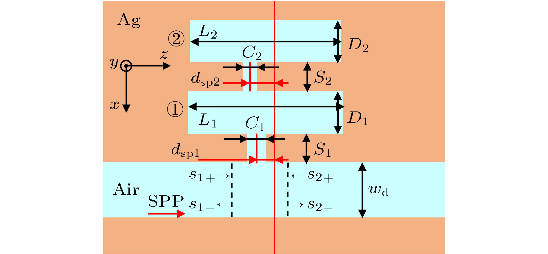
图 3 金属波导-双微腔侧边耦合结构示意图. 在图1的基础上再加入一个谐振腔, 并为两个谐振腔编号为①与②. 靠近波导的为1号微腔, 所有的结构参数的尾数都为1; 远离波导的为2号谐振腔, 所有的结构参数的尾数为2. 空气层厚度为wd
Figure 3. The schematic diagram of metal waveguide-double microcavities side-coupled structure. A other microcavity is introduced into the structure shown in Fig.1. The two microcavities are numbered as ① and ②, respectively. The width of air layer is wd.
图 4 波导-双微腔结构的透射谱. 其中, 红色实线表示FDFD方法得到的结果, 蓝色圆点为TCMT方法得到的结果. 为了便于比较, 单个波导-微腔结构的透射谱在图中以黑色虚线表示; (b)波导-双微腔结构中, 透射波的位相变化情况. 数值模拟中, 结构的几何参数为L1 = 650 nm, D1 = 200 nm, S1 = 200 nm, C1 = 100 nm, dsp1 = 120 nm, L2 = 625 nm, D2 = 200 nm, S2 = 250 nm, C2 = 40 nm, dsp2 = 80 nm, wd = 200 nm.
Figure 4. (a) The transmittance spectra of waveguide-microcavities structure. The red line and blue dotted line denote the results obtained from FDFD simulation and TCMT, respectively. For comparison, the transmittance spectra of the single waveguide-microcavity are shown with black dashed line; (b) for waveguide-microcavities structure, the phase of output wave versus the wavelength. In simulation, the parameters of structure are L1 = 650 nm, D1 = 200 nm, S1 = 200 nm, C1 = 100 nm, dsp1 = 120 nm, L2 = 625 nm, D2 = 200 nm, S2 = 250 nm, C2 = 40 nm, dsp2 = 80 nm and wd = 200 nm.
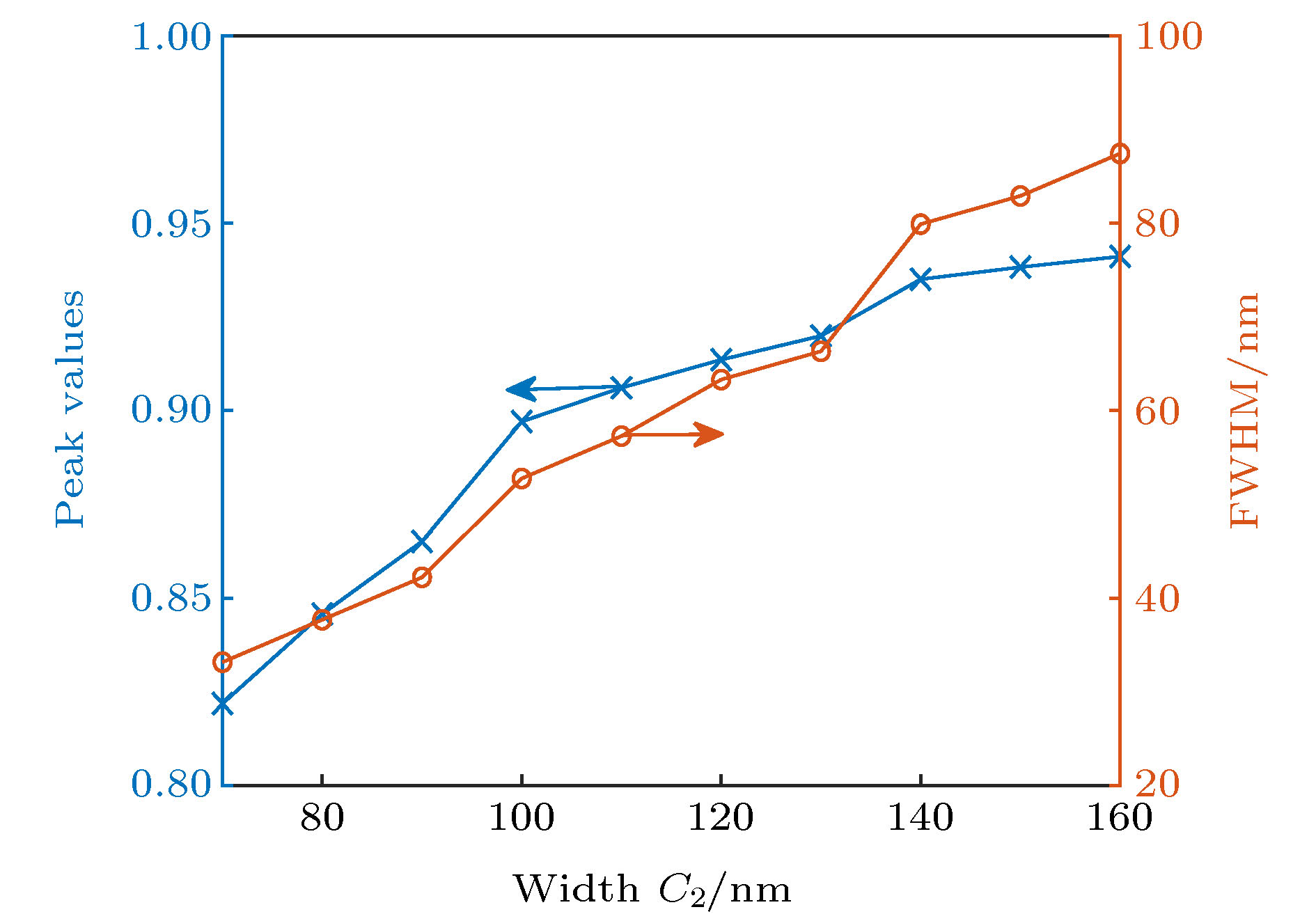
图 5 类EIT窗口透射峰值和FWHM与狭缝开口宽度C2的关系. 结构的其他参数为L1 = 650 nm, D1 = 200 nm, S1 = 200 nm, C1 = 100 nm, dsp1 = 120 nm, L2 = 625 nm, D2 = 200 nm, S2 = 250 nm, dsp2 = 80 nm, wd = 200 nm
Figure 5. The peak value of transmission and the FWHM of EIT window versus the width C2 of slit. In simulation, the geometrical parameters of structure are L1 = 650 nm, D1 = 200 nm, S1 = 200 nm, C1 = 100 nm, dsp1 = 120 nm, L2 = 625 nm, D2 = 200 nm, S2 = 250 nm, dsp2 = 80 nm and wd = 200 nm.
-
[1] Harris S E, Field J E, Imamoglu A 1990 Phys. Rev. Lett. 64 1107
 Google Scholar
[2] Zhang S, Genov D A, Wang Y, Liu M, Zhang X 2008 Phys. Rev. Lett. 101 047401
 Google Scholar
[3] Xu Q, Sandhu S, Povinelli M L, Shakya J, Fan S, Lipson M 2006 Phys. Rev. Lett. 96 123901
 Google Scholar
[4] Chen H, Chan C T 2007 Appl. Phys. Lett. 91 183518
 Google Scholar
[5] Zhang Z, Zhang L, Li H, Chen H 2014 Appl. Phys. Lett. 104 231114
 Google Scholar
[6] Chen J, Wang C, Zhang R, Xiao J 2012 Opt. Lett. 37 5133
 Google Scholar
[7] Yun B, Hu G, Cui Y 2013 Plasmonics 8 267
[8] Lu Q, Wang Z, Huang Q, Jiang W, Wu Z, Wang Y, Xia J 2017 J. Lightwave Technol. 35 1710
 Google Scholar
[9] Rumpf R C 2012 Prog. Electromagn. Res. B 36 221
 Google Scholar
[10] Johnson P B, Christy R W 1972 Phys. Rev. B 6 4370
 Google Scholar
[11] Mario L Y, Chin M K 2008 Opt. Express 16 1796
 Google Scholar
[12] Han Z, I.Bozhevolnyi S 2011 Opt. Express 19 3251
 Google Scholar
[13] 宁仁霞, 鲍婕, 焦铮 2017 66 100202
 Google Scholar
Ning R X, Bao J, Jiao Z 2017 Acta Phys. Sin. 66 100202
 Google Scholar
[14] Haddadpour A, Nezhad V F, Yu Z, Veronis G 2016 Opt. Lett. 41 4340
 Google Scholar
[15] Yu Z, Veronis G, Fan S 2008 Appl. Phys. Lett. 92 041117
 Google Scholar
[16] Fan S, Suh W, Joannopoulos J D 2003 J. Opt. Soc. Am. A 20 569
 Google Scholar
[17] Suh W, Wang Z, Fan S 2004 IEEE J. Quantum Electron. 40 1511
 Google Scholar
[18] Chen J, Wang P, Zhang Z M, Lu Y, Ming H 2011 Phys. Rev. E 84 026603
 Google Scholar
[19] 王辉, 沙威, 黄志祥, 吴先良, 沈晶 2014 63 184210
 Google Scholar
Wang H, Sha W, Huang Z, Wu X, Shen J 2014 Acta Phys. Sin. 63 184210
 Google Scholar
[20] Zhang Z, Ng G I, Hu T, Qiu H, Guo X, Wang W, Rouifed M S, Liu C, Wang H 2017 Appl. Phys. Lett. 111 081105
 Google Scholar
Catalog
Metrics
- Abstract views: 10433
- PDF Downloads: 251
- Cited By: 0


 DownLoad:


