-
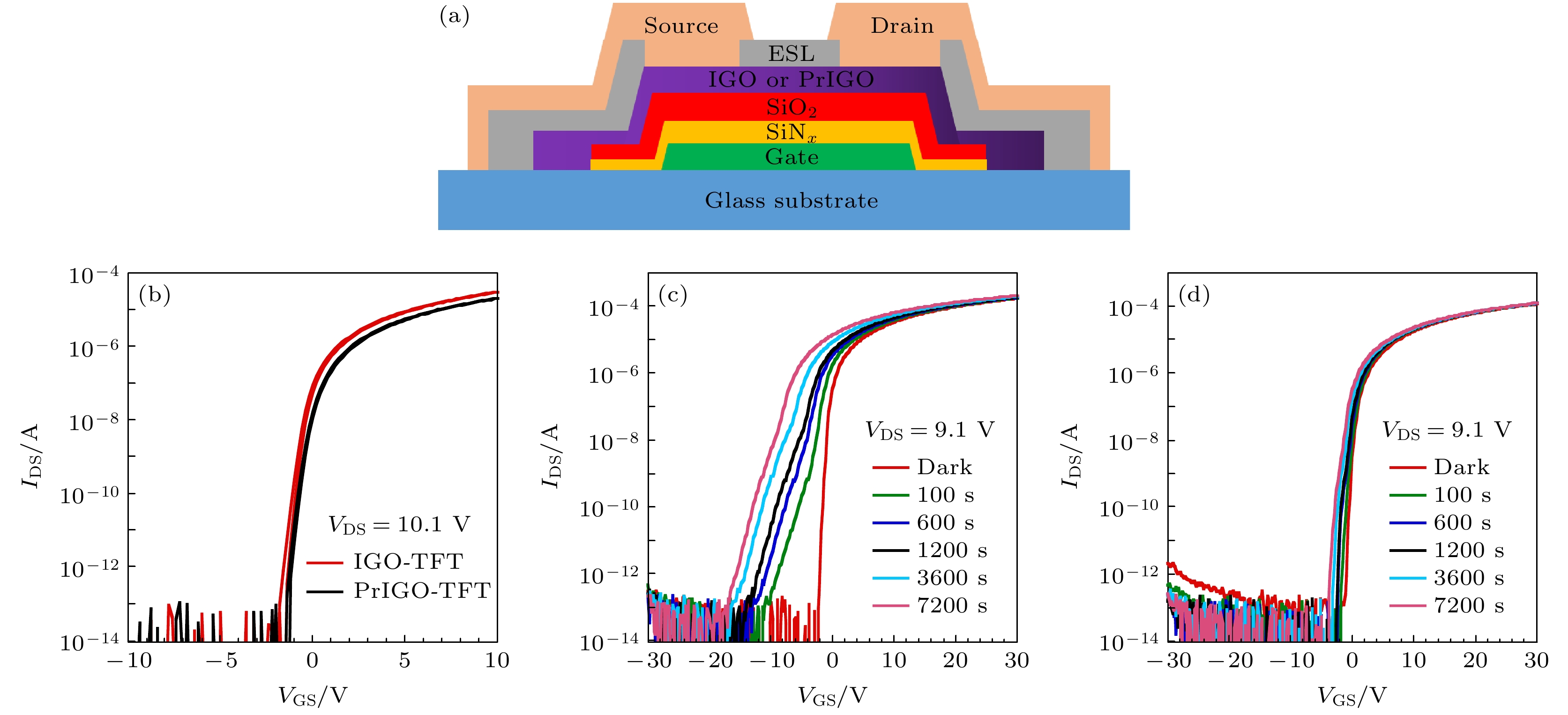
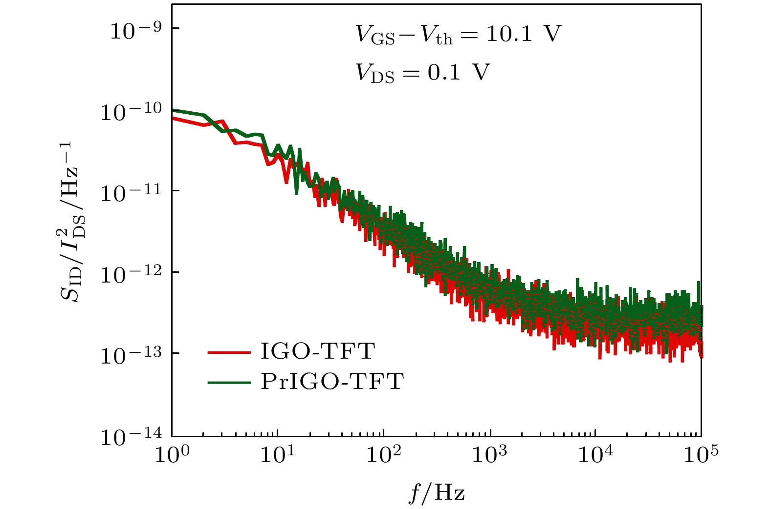
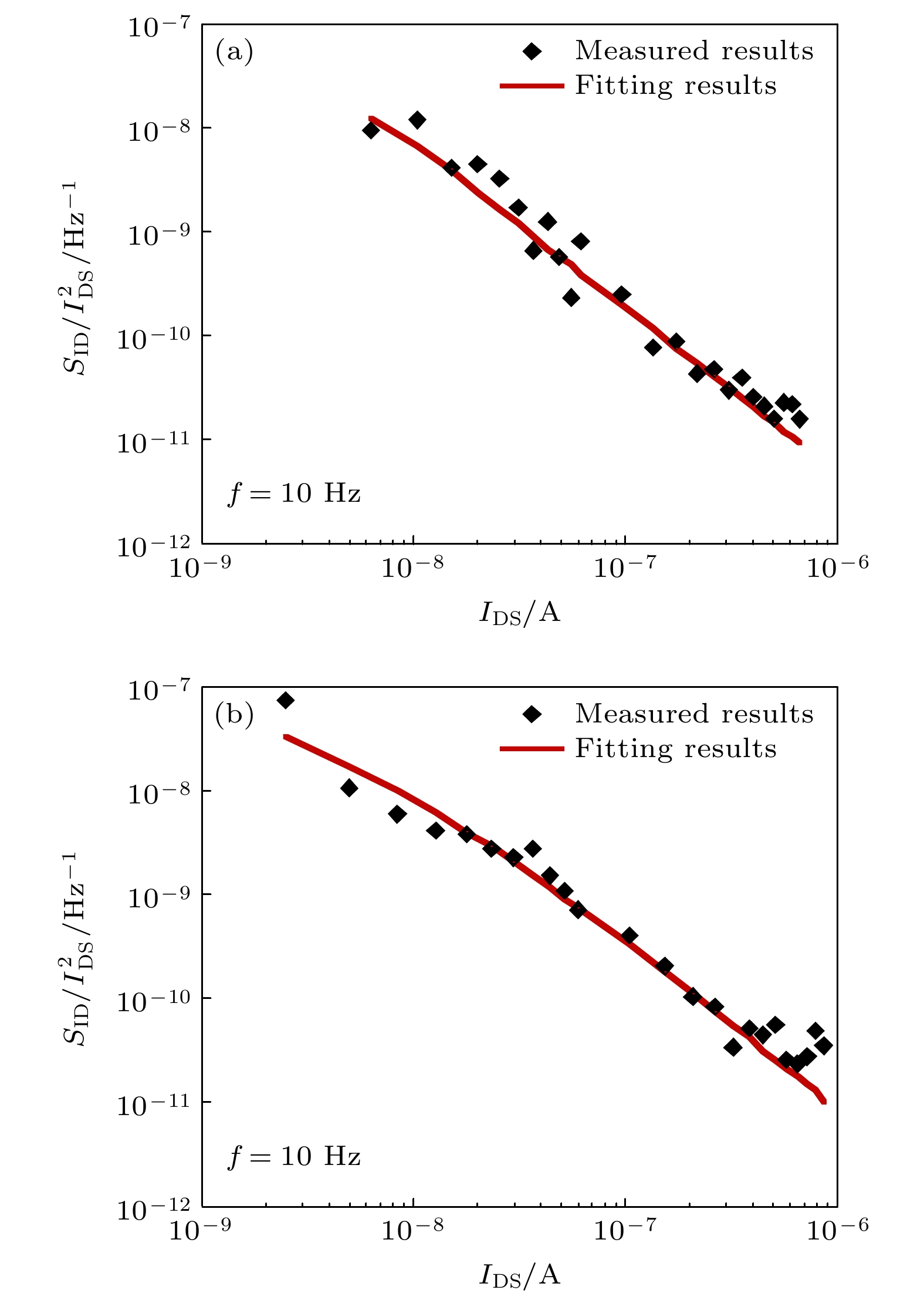
本文研究了镨掺杂铟镓氧化物 (PrIGO)薄膜晶体管 (thin film transistor, TFT) 的低频噪声特性. 根据低频噪声测试分析结果得知: IGO-TFT和PrIGO-TFT器件沟道电流的功率谱密度与频率的关系均满足1/fγ (γ ≈ 0.8) 的关系, 符合载流子数涨落模型. 通过研究不同沟道长度对器件低频噪声的影响, 明确了器件的噪声主要来源于沟道区而非源/漏接触区. 基于载流子数涨落模型, 提取界面处的缺陷态, 发现Pr元素掺杂会在IGO体系中诱导出缺陷态. 而该缺陷态可以作为电离氧空位和电子的复合中心, 进而改善氧化物TFT器件中由氧空位所导致的光照负偏压 (negative bias illumination stability, NBIS) 稳定性问题.Metal oxide thin film transistors (MOTFTs) have been extensively investigated in the display industry because of their attractive characteristics, including high performances, low processing temperatures, and simple fabrication. However, under the actual working condition, the characteristics of TFTs are easily affected by the light irradiation caused the negative gate bias stress (NBIS). Therefore, the NBIS stability of MOTFT is a crucial issue that must be solved before their commercialization into an optoelectronic device. In this article, praseodymium-doped indium gallium oxide (PrIGO) is employed as the channel layer of thin film transistor (TFT). The TFTs with Pr doping exhibit a remarkable enhancement in NBIS stability. The structure and chemical composition of PrIGO film are analyzed by X-ray diffraction (XRD) and X-ray photoelectron spectroscopy (XPS), respectively. Besides, to further explore the mechanism for the improvement of NBIS stability, the low-frequency noise characteristics of IGO-TFT device and PrIGO-TFT device are studied. According to the low frequency noise characterization and analysis results, the correspondence between the normalized drain current noise power spectral density(
$ S_{\rm ID}/I_{\rm DS}^2 $ ) and frequency shows 1/fγ (γ ≈ 0.8) low frequency noise behavior for IGO-TFT device and PrIGO-TFT device. In addition, by studying the influences of different channel lengths on the low frequency noise of the IGO-TFT and PrIGO-TFT devices, it can be concluded that the low frequency noise of the device comes mainly from the channel region rather than from the source/drain contact region. In the linear region of the IGO-TFT device and PrIGO-TFT device, according to the linear fitting of the$ S_{\rm ID}/I_{\rm DS}^2 $ versus the overdrive voltage (VGS – Vth), it is proved that the low frequency noise of the IGO-TFT device and the PrIGO-TFT device are mainly affected by the carrier number fluctuation model. Finally, based on the carrier number fluctuation model, the defect state density at the interface between active layer and gate insulating layer is extracted to be 7.76 × 1017 cm–3·eV–1 and 9.55 × 1017 cm–3·eV–1 for IGO-TFT and PrIGO-TFT devices, respectively. We speculate that the Pr element can induce defect states in the IGO system, and the trap states induced by Pr ions facilitate the capture of free electrons by positively charged oxygen vacancies, which lead the photo-induced carrier in conduction band to be suppressed.-
Keywords:
- indium gallium oxide /
- thin film transistor /
- low-frequency noise
[1] Nomura K, Ohta H, Takagi A, Kamiya T, Hirano M, Hosono H 2004 Nature 432 488
 Google Scholar
[2] Ebata K, Tomai S, Tsuruma Y, Iitsuka T, Matsuzaki S, Yano K 2012 Appl. Phys. Express 5 11102
 Google Scholar
[3] Xiao P, Dong T, Lan L, Lin Z, Song W, Song E, Sun S, Li Y, Gao P, Luo D, Xu M, Peng J 2016 Phys. Status Solidi RRL 10 493
 Google Scholar
[4] Park H, Bae J, Kang H, Kim D H, Jung P, Park H, Lee S, Bae J U, Yoon S Y, Kang I 2019 SID Int. Symp. Digest Techn. Papers 50 1222
 Google Scholar
[5] Cheng Y, Chang S, Chang S 2019 Mater. Res. Express 6 106445
 Google Scholar
[6] Chen T, Chang T, Hsieh T, Tsai C, Chen S, Lin C, Hung M, Tu C, Chang J, Chen P 2010 Appl. Phys. Lett. 97 192103
 Google Scholar
[7] Chowdhury M D H, Migliorato P, Jang J 2010 Appl. Phys. Lett. 97 173506
 Google Scholar
[8] Ryu B, Noh H, Choi E, Chang K J 2010 Appl. Phys. Lett. 97 22108
 Google Scholar
[9] Xu H, Xu M, Li M, Chen Z, Zou J, Wu W, Qiao X, Tao H, Wang L, Ning H, Ma D, Peng J 2019 ACS Appl. Mater. Interfaces. 11 5232
 Google Scholar
[10] Fung T, Baek G, Kanicki J 2010 J. Appl. Phys. 108 74518
 Google Scholar
[11] Wang L, Liu Y, Geng K, Chen Y, En Y 2018 Chin. Phys. B 27 68504
 Google Scholar
[12] Cho I, Cheong W, Hwang C, Lee J, Kwon H, Lee J 2009 IEEE Electron Device Lett. 30 828
 Google Scholar
[13] Song A, Javaid K, Liang Y, Wu W, Yu J, Liang L, Zhang H, Lan L, Chang T, Cao H 2018 Phys. Status Solidi RRL 12 1800034
 Google Scholar
[14] 王静, 刘远, 刘玉荣, 吴为敬, 罗心月, 刘凯, 李斌, 恩云飞 2016 65 128501
 Google Scholar
Wang J, Liu Y, Liu Y R, Wu W J, Luo X Y, Liu K, Li B, En Y F 2016 Acta Phys. Sin. 65 128501
 Google Scholar
[15] 刘远, 何红宇, 陈荣盛, 李斌, 恩云飞, 陈义强 2017 66 237101
 Google Scholar
Liu Y, He H Y, Chen R S, Li B, En Y F, Chen Y Q 2017 Acta Phys. Sin. 66 237101
 Google Scholar
[16] Deen M J, Rumyantsev S L, Landheer D, Xu D X 2000 Appl. Phys. Lett. 77 2234
 Google Scholar
[17] Choi H, Jeon S, Kim H, Shin J, Kim C, Chung U 2011 IEEE Electron Device Lett. 32 1083
 Google Scholar
[18] Liu Y, He H, Chen R, En Y, Li B, Chen Y 2018 IEEE J. Electron Devi. 6 271
 Google Scholar
[19] Kim S, Jeon Y, Lee J, Ahn B D, Park S Y, Park J, Kim J H, Park J, Kim D M, Kim D H 2010 IEEE Electron Device Lett. 31 1236
[20] Vandamme L K J, Hooge F N 2008 IEEE Trans. Electron Devices 55 3070
 Google Scholar
[21] Cai M, Yao R 2017 J. Appl. Phys. 122 154503
 Google Scholar
[22] Ghibaudo G, Roux O, Nguyen-Duc C, Balestra F, Brini J 1991 Phys. Status Solidi A 124 571
 Google Scholar
[23] Petit L, Svane A, Szotek Z, Temmerman W M 2005 Phys. Rev. B 72 205118
 Google Scholar
-
图 2 IGO和PrIGO薄膜 (a) X射线衍射谱图; (b) 紫外-可见透射光谱图 (插图为 (αhv)2随hv变化曲线); (c) X射线光电子能谱图 (插图为局部放大图)
Fig. 2. (a) X-ray diffraction spectra, (b) UV-visible transmission spectra (the inset shows the curve of (αhv)2 varying with hv) and (c) X-ray photoelectron spectroscopy (the inset is a partial enlarged view) of IGO and PrIGO thin film.
表 1 IGO和PrIGO薄膜中各元素的百分比含量
Table 1. Percentage contents of each element in IGO and PrIGO films.
Element/at.% Pr In Ga O PrIGO 2.86 28.76 15.10 51.89 IGO — 30.93 15.51 51.85 -
[1] Nomura K, Ohta H, Takagi A, Kamiya T, Hirano M, Hosono H 2004 Nature 432 488
 Google Scholar
[2] Ebata K, Tomai S, Tsuruma Y, Iitsuka T, Matsuzaki S, Yano K 2012 Appl. Phys. Express 5 11102
 Google Scholar
[3] Xiao P, Dong T, Lan L, Lin Z, Song W, Song E, Sun S, Li Y, Gao P, Luo D, Xu M, Peng J 2016 Phys. Status Solidi RRL 10 493
 Google Scholar
[4] Park H, Bae J, Kang H, Kim D H, Jung P, Park H, Lee S, Bae J U, Yoon S Y, Kang I 2019 SID Int. Symp. Digest Techn. Papers 50 1222
 Google Scholar
[5] Cheng Y, Chang S, Chang S 2019 Mater. Res. Express 6 106445
 Google Scholar
[6] Chen T, Chang T, Hsieh T, Tsai C, Chen S, Lin C, Hung M, Tu C, Chang J, Chen P 2010 Appl. Phys. Lett. 97 192103
 Google Scholar
[7] Chowdhury M D H, Migliorato P, Jang J 2010 Appl. Phys. Lett. 97 173506
 Google Scholar
[8] Ryu B, Noh H, Choi E, Chang K J 2010 Appl. Phys. Lett. 97 22108
 Google Scholar
[9] Xu H, Xu M, Li M, Chen Z, Zou J, Wu W, Qiao X, Tao H, Wang L, Ning H, Ma D, Peng J 2019 ACS Appl. Mater. Interfaces. 11 5232
 Google Scholar
[10] Fung T, Baek G, Kanicki J 2010 J. Appl. Phys. 108 74518
 Google Scholar
[11] Wang L, Liu Y, Geng K, Chen Y, En Y 2018 Chin. Phys. B 27 68504
 Google Scholar
[12] Cho I, Cheong W, Hwang C, Lee J, Kwon H, Lee J 2009 IEEE Electron Device Lett. 30 828
 Google Scholar
[13] Song A, Javaid K, Liang Y, Wu W, Yu J, Liang L, Zhang H, Lan L, Chang T, Cao H 2018 Phys. Status Solidi RRL 12 1800034
 Google Scholar
[14] 王静, 刘远, 刘玉荣, 吴为敬, 罗心月, 刘凯, 李斌, 恩云飞 2016 65 128501
 Google Scholar
Wang J, Liu Y, Liu Y R, Wu W J, Luo X Y, Liu K, Li B, En Y F 2016 Acta Phys. Sin. 65 128501
 Google Scholar
[15] 刘远, 何红宇, 陈荣盛, 李斌, 恩云飞, 陈义强 2017 66 237101
 Google Scholar
Liu Y, He H Y, Chen R S, Li B, En Y F, Chen Y Q 2017 Acta Phys. Sin. 66 237101
 Google Scholar
[16] Deen M J, Rumyantsev S L, Landheer D, Xu D X 2000 Appl. Phys. Lett. 77 2234
 Google Scholar
[17] Choi H, Jeon S, Kim H, Shin J, Kim C, Chung U 2011 IEEE Electron Device Lett. 32 1083
 Google Scholar
[18] Liu Y, He H, Chen R, En Y, Li B, Chen Y 2018 IEEE J. Electron Devi. 6 271
 Google Scholar
[19] Kim S, Jeon Y, Lee J, Ahn B D, Park S Y, Park J, Kim J H, Park J, Kim D M, Kim D H 2010 IEEE Electron Device Lett. 31 1236
[20] Vandamme L K J, Hooge F N 2008 IEEE Trans. Electron Devices 55 3070
 Google Scholar
[21] Cai M, Yao R 2017 J. Appl. Phys. 122 154503
 Google Scholar
[22] Ghibaudo G, Roux O, Nguyen-Duc C, Balestra F, Brini J 1991 Phys. Status Solidi A 124 571
 Google Scholar
[23] Petit L, Svane A, Szotek Z, Temmerman W M 2005 Phys. Rev. B 72 205118
 Google Scholar
计量
- 文章访问数: 9513
- PDF下载量: 172
- 被引次数: 0


 下载:
下载:


