-
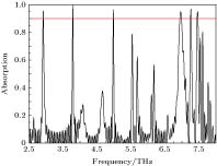
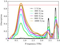
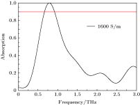
随着频谱资源的日益稀缺, 太赫兹波技术在近十几年的时间里得到了越来越多的关注, 并取得了巨大的进展. 由于高吸收、超薄厚度、频率选择性和设计灵活性等优势, 超材料吸收器在太赫兹波段备受关注. 本文设计了一种“T”型结构的超材料太赫兹吸收器, 同时获得了太赫兹多频吸收器和太赫兹波宽频可调谐吸收器. 它们结构参数一致, 唯一的区别是在太赫兹波宽频可调谐吸收器的顶端超材料层上添加了一块方形光敏硅. 这种吸收器都是三层结构, 均由金属基板、匹配电介质层以及顶端超材料层组成. 仿真结果表明, 太赫兹波多频吸收器拥有6个吸收率超过90%的吸收峰, 其平均吸收率高达96.34%. 而太赫兹波宽频可调谐吸收器通过改变硅电导率, 可以控制吸收频带的存在与否, 同时可以调整吸收峰的频率位置, 使吸收峰频率在一个频带宽度大约为30 GHz的范围内调整. 当硅的电导率为1600 S/m时, 吸收率超过90%的频带宽度达到240 GHz, 而且其峰值吸收率达到99.998%.With the increasing scarcity of spectrum resources, terahertz wave technologies have attracted more and more attention in recent decades, and have made tremendous progress. Terahertz wave referring to electromagnetic waves with a frequency in a range of 0.1-10 THz has a wide range of applications in wireless communication, nondestructive imaging and remote sensing. Due to the advantages of high absorption, ultra-thin thickness, frequency selectivity and design flexibility, metamaterial absorbers have attracted more attention in terahertz band. In this paper, two terahertz metamaterial absorbers with different performances are designed which are named “T” terahertz multi-band absorber and “T” terahertz tunable broadband absorber, respectively. The absorbers are both comprised of three layers: metal substrate, matched dielectric layer and surface metamaterial layer. The main structures of these two absorbers are composed of four T-shape Au plates on the top of polyimide dielectric layer and an Au sheet acting as a bottom layer. The only difference between these two absorbers is that the terahertz broadband tunable absorber possesses a square photosensitive silicon in the metamaterial layer. The simulations results show that the terahertz multi-band absorber has six absorption peaks at 2.918, 3.7925, 4.986, 6.966, 7.2685, and 7.4665 THz, with the absorptivity peaks of 95.631%, 99.508%, 96.34%, 94.835%, 96.485%, 94.732%, respectively, and the average absorption rate is 96.26%. Terahertz tunable broadband absorber has the characteristics of broadband absorption. When the conductivity of silicon is 1600 S/m, the absorber reaches its absorption peak at 0.786 THz with the absorptivity of 99.998%, and the frequency bandwidth with the absorption rate exceeding 90% reaches 240 GHz. The more interesting thing is that by changing the conductivity of silicon, the terahertz tunable broadband absorber shows the ability to dynamically control the existence of absorption band and adjust the frequency position of absorption peak. For terahertz tunable broadband absorber, the frequency of absorption peak can be regulated in a bandwidth of about 30 GHz. The terahertz wave absorbers designed in this paper possess rather simple structures, therefore the proposed absorbers are easy to fabricate. Because of these excellent properties, the absorbers may have potential applications in optical switch, optical detection, optical imaging, band-stop devices, and other fields.
-
Keywords:
- terahertz absorber /
- multi-band absorber /
- tunable broadband /
- metamaterial
[1] Landy N I, Sajuyigbe S, Mock J J, Smith D R, Padilla W J 2008 Phys. Rev. Lett. 100 207402
 Google Scholar
[2] 赵碧辉, 文岐业, 谢云松 2011 电子元件与材料 30 82
 Google Scholar
Zhao B H, Wen Q Y, Xie Y S 2011 Electr. Comp. Mater. 30 82
 Google Scholar
[3] 沈晓鹏, 崔铁军, 叶建祥 2012 61 058101
 Google Scholar
Shen X P, Cui T J, Ye J X 2012 Acta Phys. Sin. 61 058101
 Google Scholar
[4] 保石, 罗春荣, 张燕萍, 赵晓鹏 2010 59 3187
 Google Scholar
Bao S, Luo C R, Zhang Y P, Zhao X P 2010 Acta Phys. Sin. 59 3187
 Google Scholar
[5] 莫漫漫, 文岐业, 陈智, 杨青慧, 李胜, 荆玉兰, 张怀武 2013 62 237801
 Google Scholar
Mo M M, Wen Q Y, Chen Z, Yang Q H, Li S, Jing Y L, Zhang H W 2013 Acta Phys. Sin. 62 237801
 Google Scholar
[6] Zhai Z, Zhang L, Li X, Xiao S 2019 Opt. Commun. 431 199
 Google Scholar
[7] Andryieuski A, Lavrinenko A V 2013 Opt. Express 21 9144
 Google Scholar
[8] Zhang Y, Feng Y, Zhu B, Zhao J, Jiang T 2014 Opt. Express 22 22743
 Google Scholar
[9] 程伟, 李九生 2013 电子元件与材料 32 34
 Google Scholar
Cheng W, Li J S 2013 Electr. Comp. Mater. 32 34
 Google Scholar
[10] Zhao X, Wang Y, Schalch J, Duan G, Cremin K, Zhang J D, Chen C X, Averitt R D, Zhang X 2019 ACS Photon. 6 830
[11] Chen M, Yan W, Tong X, Zeng L, Li Z, Yang F 2019 J. Opt. 21 035102
 Google Scholar
[12] Faraji M, Moravvej-Farshi M K, Yousefi L 2015 Opt. Commun. 355 352
 Google Scholar
[13] Yan H, Li X, Chandra B, Tulevski G, Wu Y, Freitag M, Zhu W, Avouris P, Xia F 2012 Nat. Nanotechnol. 7 330
 Google Scholar
[14] Kim K S, Zhao Y, Jang H, Lee S Y, Kim J M, Kim K S, Ahn J H, Kim P, Choi J J, Hong B H 2009 Nature 457 706
 Google Scholar
[15] 梁兰菊, 闫昕, 姚建铨 2016 枣庄学院学报 33 10
 Google Scholar
Liang L J, Yao J Q 2016 J. Zaozhuang Univ. 33 10
 Google Scholar
[16] Chen L, Wei Y M, Zang X F, Zhu Y M, Zhuang S L 2016 Sci. Rep. 6 22027
 Google Scholar
[17] Chen L, Liao D G, Guo X G, Zhao J Y, Zhu Y M, Zhuang S L 2019 Front. Inform. Tech. El. 20 591
 Google Scholar
[18] 陈康, 文岐业, 张怀武 2011 电子元件与材料 30 56
 Google Scholar
Chen K, Wen Q Y, Zhang H W 2011 Electr. Comp. Mater. 30 56
 Google Scholar
[19] 颜世桃 2016 硕士学位论文 (哈尔滨: 哈尔滨理工大学)
Yao S T 2016 M. S. Thesis (Haerbin: Harbin University of Science and Technology) (in Chinese)
[20] He X J, Yan S T, Ma Q X, Zhang Q F, Jia P, Wu F M, Jiang J X 2015 Opt. Commun. 340 44
 Google Scholar
[21] Gong C, Zhan M Z, Yang J, Wang Z G, Liu H T, Zhao Y J 2016 Sci. Rep. 6 32466
 Google Scholar
-
图 1 超材料太赫兹波吸收器结构示意图 (a) 多频吸收器示意图; (b) 宽频可调谐吸收器示意图; (c) 吸收器剖面图; (d) 吸收器表面结构图
Fig. 1. Structural schematic diagram of metamaterial terahertz wave absorbers: (a) Schematic diagram of multi-band absorber; (b) schematic diagram of broadband tunable absorber; (c) profile of absorber; (d) surface structure of absorber.
表 1 超材料太赫兹吸收器的结构尺寸
Table 1. Structure dimensions of metamaterial terahertz absorber
参数 a b w p h1 h2 h3 取值/μm 12 4 8 32 1 30 1 -
[1] Landy N I, Sajuyigbe S, Mock J J, Smith D R, Padilla W J 2008 Phys. Rev. Lett. 100 207402
 Google Scholar
[2] 赵碧辉, 文岐业, 谢云松 2011 电子元件与材料 30 82
 Google Scholar
Zhao B H, Wen Q Y, Xie Y S 2011 Electr. Comp. Mater. 30 82
 Google Scholar
[3] 沈晓鹏, 崔铁军, 叶建祥 2012 61 058101
 Google Scholar
Shen X P, Cui T J, Ye J X 2012 Acta Phys. Sin. 61 058101
 Google Scholar
[4] 保石, 罗春荣, 张燕萍, 赵晓鹏 2010 59 3187
 Google Scholar
Bao S, Luo C R, Zhang Y P, Zhao X P 2010 Acta Phys. Sin. 59 3187
 Google Scholar
[5] 莫漫漫, 文岐业, 陈智, 杨青慧, 李胜, 荆玉兰, 张怀武 2013 62 237801
 Google Scholar
Mo M M, Wen Q Y, Chen Z, Yang Q H, Li S, Jing Y L, Zhang H W 2013 Acta Phys. Sin. 62 237801
 Google Scholar
[6] Zhai Z, Zhang L, Li X, Xiao S 2019 Opt. Commun. 431 199
 Google Scholar
[7] Andryieuski A, Lavrinenko A V 2013 Opt. Express 21 9144
 Google Scholar
[8] Zhang Y, Feng Y, Zhu B, Zhao J, Jiang T 2014 Opt. Express 22 22743
 Google Scholar
[9] 程伟, 李九生 2013 电子元件与材料 32 34
 Google Scholar
Cheng W, Li J S 2013 Electr. Comp. Mater. 32 34
 Google Scholar
[10] Zhao X, Wang Y, Schalch J, Duan G, Cremin K, Zhang J D, Chen C X, Averitt R D, Zhang X 2019 ACS Photon. 6 830
[11] Chen M, Yan W, Tong X, Zeng L, Li Z, Yang F 2019 J. Opt. 21 035102
 Google Scholar
[12] Faraji M, Moravvej-Farshi M K, Yousefi L 2015 Opt. Commun. 355 352
 Google Scholar
[13] Yan H, Li X, Chandra B, Tulevski G, Wu Y, Freitag M, Zhu W, Avouris P, Xia F 2012 Nat. Nanotechnol. 7 330
 Google Scholar
[14] Kim K S, Zhao Y, Jang H, Lee S Y, Kim J M, Kim K S, Ahn J H, Kim P, Choi J J, Hong B H 2009 Nature 457 706
 Google Scholar
[15] 梁兰菊, 闫昕, 姚建铨 2016 枣庄学院学报 33 10
 Google Scholar
Liang L J, Yao J Q 2016 J. Zaozhuang Univ. 33 10
 Google Scholar
[16] Chen L, Wei Y M, Zang X F, Zhu Y M, Zhuang S L 2016 Sci. Rep. 6 22027
 Google Scholar
[17] Chen L, Liao D G, Guo X G, Zhao J Y, Zhu Y M, Zhuang S L 2019 Front. Inform. Tech. El. 20 591
 Google Scholar
[18] 陈康, 文岐业, 张怀武 2011 电子元件与材料 30 56
 Google Scholar
Chen K, Wen Q Y, Zhang H W 2011 Electr. Comp. Mater. 30 56
 Google Scholar
[19] 颜世桃 2016 硕士学位论文 (哈尔滨: 哈尔滨理工大学)
Yao S T 2016 M. S. Thesis (Haerbin: Harbin University of Science and Technology) (in Chinese)
[20] He X J, Yan S T, Ma Q X, Zhang Q F, Jia P, Wu F M, Jiang J X 2015 Opt. Commun. 340 44
 Google Scholar
[21] Gong C, Zhan M Z, Yang J, Wang Z G, Liu H T, Zhao Y J 2016 Sci. Rep. 6 32466
 Google Scholar
计量
- 文章访问数: 14751
- PDF下载量: 468
- 被引次数: 0


 下载:
下载:


