-
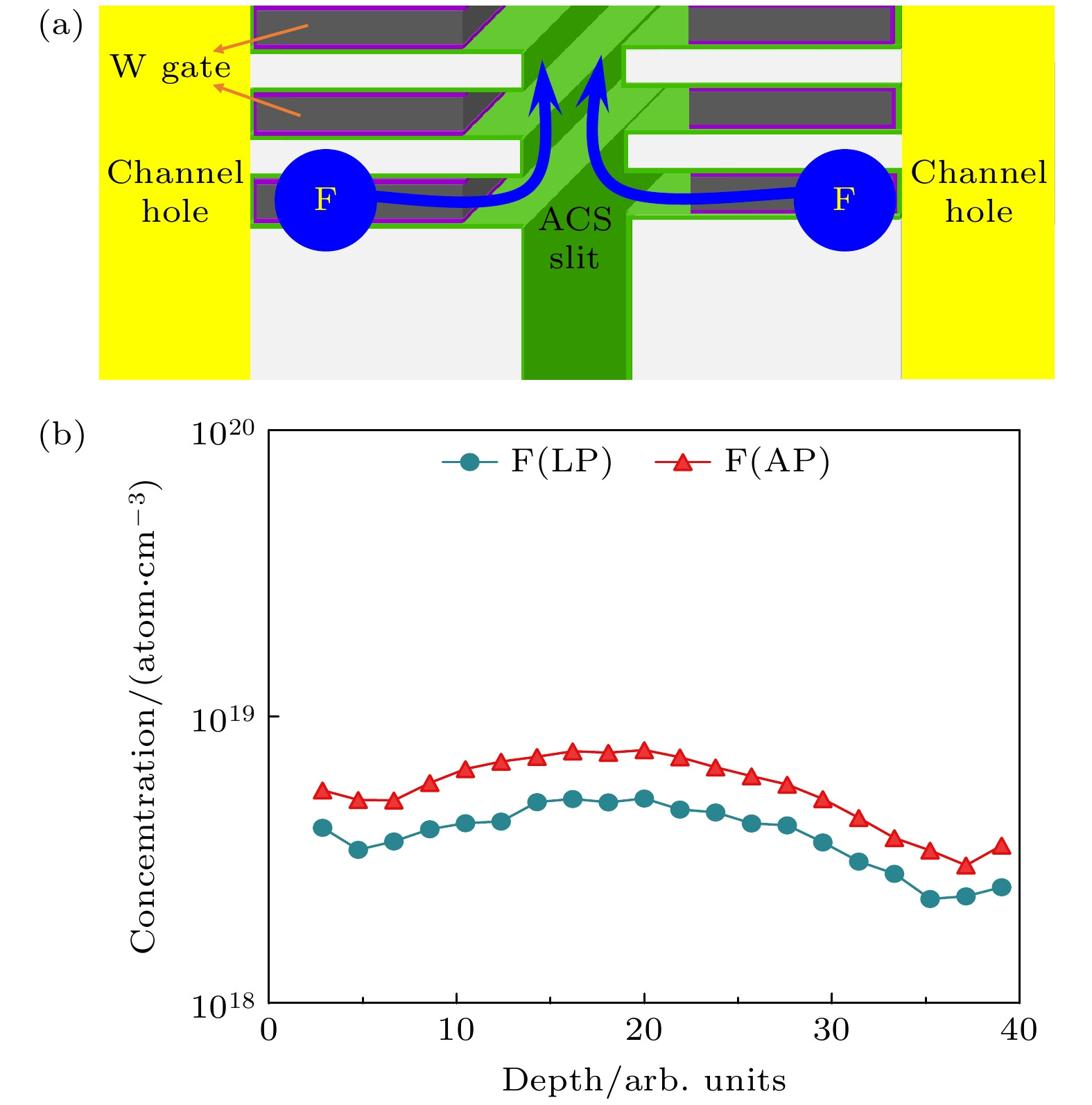
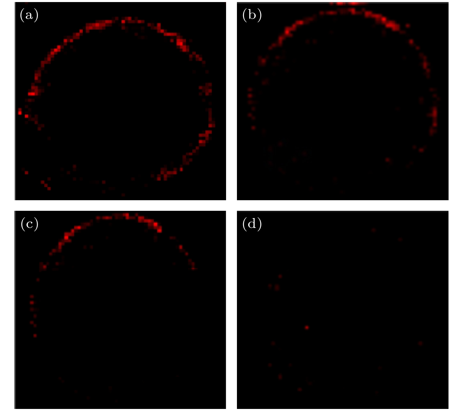
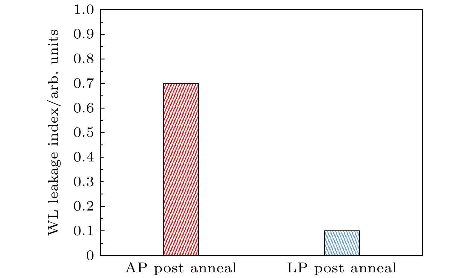
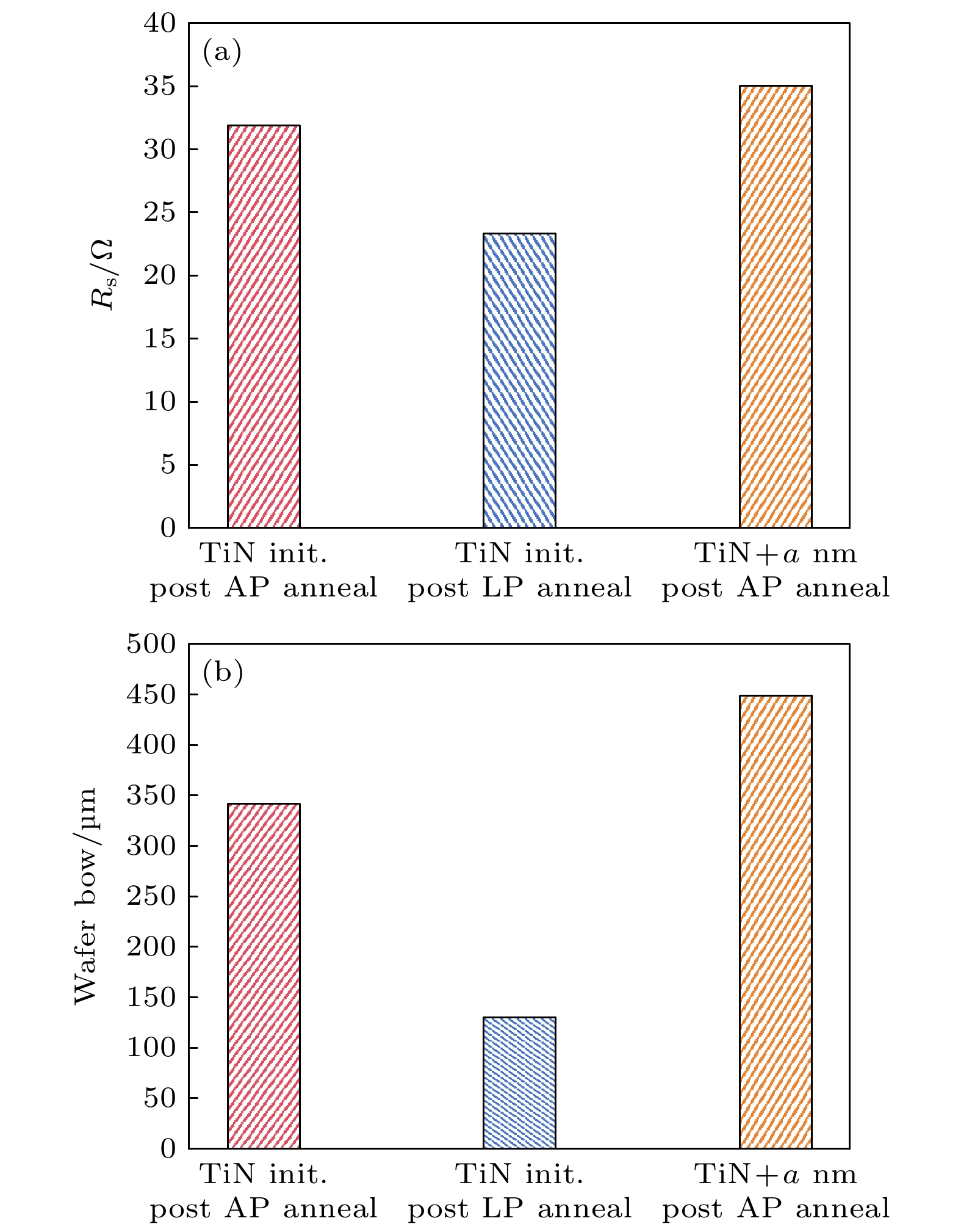
In this work, the influence of fluorine (F) erosion on tungsten (W) gate process is studied, and the measure to mitigate the word line (WL) leakage resulting from F erosion in 3D NAND flash memory is proposed. As the number of layers in 3D NAND increases, the tungsten (W) gate word line (WL) layer fill process becomes more challenging in the post-gate process. As the fill path length increases, the tungsten gates become more susceptible to voiding during deposition, resulting in the accumulation of fluorine (F) by-products, and causing fluorine attack issues. In particular, under the influence of subsequent high-temperature processes, the by-products containing fluorine can diffuse into the surrounding structure and corrode the surrounding oxide layer. This leads to WL leakage, thereby affecting device yield and reliability. This paper begins by analyzing the microscopic principles of fluorine erosion in 3D NAND. We also propose a low-pressure annealing method to address the issue of fluorine erosion. Then, we conduct the experiments on annealing planar thin film stacks and 3D filled structures under atmospheric condition and low-pressure condition. We use various methods to characterize the concentration and distribution of residual fluorine elements. The experimental results demonstrate that under appropriate conditions, the residual fluorine in the tungsten gate can be effectively released by low-pressure annealing, thus reducing the leakage index of the word line. Additionally, as the outer CH is closer to the fluorine discharge channel, the influence of low-pressure annealing on the outer CH is more pronounced than on the inner CH. The low-pressure annealing can significantly reduce the fluorine content in the tungsten gate. This method can also mitigate the issue of fluorine attack oxides and reducethe WL leakage. Using low-pressure annealing treatment can also enhance the quality of 3D NAND flash technology.
[1] Compagnoni C M, Goda A, Spinelli A S, Feeley P, Lacaita A L, Visconti A 2017 Proc. IEEE 105 1609
 Google Scholar
[2] Kim H, Ahn S J, Shin Y G, Lee K, Jung E 2017 IEEE International Memory Workshop (IMW) Monterey, California, May 14–17, 2017 p1
[3] Vasilyev V, Chung S H, Song Y W 2007 Solid State Technol. 50 53
[4] Xu Q, Luo J, Wang G, Yang T, Li J, Ye T, Chen D, Zhao C 2015 Microelectron. Eng. 137 43
 Google Scholar
[5] Moon J, Lee T Y, Ahn H J, Lee T I, Hwang W S, Cho B J 2018 IEEE Trans. Electron Dev. 66 378
 Google Scholar
[6] Bakke J, Lei Y, Xu Y, Daito K, Fu X, Jian G, Wu K, Hung R, Jakkaraju R, Breil N 2016 IEEE International Interconnect Technology Conference/Advanced Metallization Conference (IITC/AMC) San Jose, California, USA, May 23–26, 2016 p108
[7] Lee J H, Hidayat R, Ramesh R, Roh H, Nandi D K, Lee W J, Kim S H 2022 Appl. Surf. Sci. 578 152062
 Google Scholar
[8] Kim C H, Rho I C, Kim S H, Han I K, Kang H S, Ryu S W, Kim H J 2009 J. Electrochem. Soc. 156 H685
 Google Scholar
[9] Subramaniyan A, Luppi D F, Makela N, Bauer L, Madan A, Murphy R, Baumann F, Kohli K, Parks C 2016 27th Annual SEMI Advanced Semiconductor Manufacturing Conference (ASMC) Saratoga Springs, New York, USA, May 16–19, 2016 p313
[10] Song Y J, Xia Z L, Hua W Y, Liu F, Huo Z L 2018 IEEE International Conference on Integrated Circuits, Technologies and Applications (ICTA) Beijing, China, November 21–23, 2018 p120
[11] Mistry K, Allen C, Auth C, Beattie B, Bergstrom D, Bost M, Brazier M, Buehler M, Cappellani A, Chau R 2007 IEEE International Electron Devices Meeting Washington, DC, December 10–12, 2007 p247
[12] Leusink G, Oosterlaken T, Janssen G, Redelaar S 1993 Thin Solid Films 228 125
 Google Scholar
[13] Kodas T T, Hampden S M J 2008 The Chemistry of Metal CVD (John Wiley & Sons) p112
[14] Klaus J, Ferro S, George S 2000 Thin Solid Films 360 145
 Google Scholar
[15] Hidayat R, Chowdhury T, Kim Y, Kim S, Mayangsari T R, Kim S H, Lee W J 2021 Appl. Surf. Sci. 538 148156
 Google Scholar
[16] Park H, Lee S, Kim H J, Woo D, Lee J M, Yoon E, Lee G D 2018 RSC Adv. 8 39039
 Google Scholar
[17] Schulze S, Wolansky D, Katzer J, Schubert M, Costina I, Mai A 2018 IEEE Trans. Semicond. Manuf. 31 528
 Google Scholar
[18] Kalanyan B, Lemaire P C, Atanasov S E, Ritz M J, Parsons G N 2016 Chem. Mater. 28 117
 Google Scholar
[19] Lee J H, Kim H W, Park I H, Cho S, Lee G S, Kim D H, Yun J G, Kim Y, Lee J D, Park B G 2006 IEEE Nanotechnology Materials and Devices Conference New York, USA, October 22–25, 2006 p638
[20] Yang Y, Zhu H, Meng X, Jin L, Wang C, Wang S, Feng S, Guo C, Zhang Y 2018 14th IEEE International Conference on Solid-State and Integrated Circuit Technology (ICSICT) Qingdao, China, October 31–November 3, 2018 p1
-
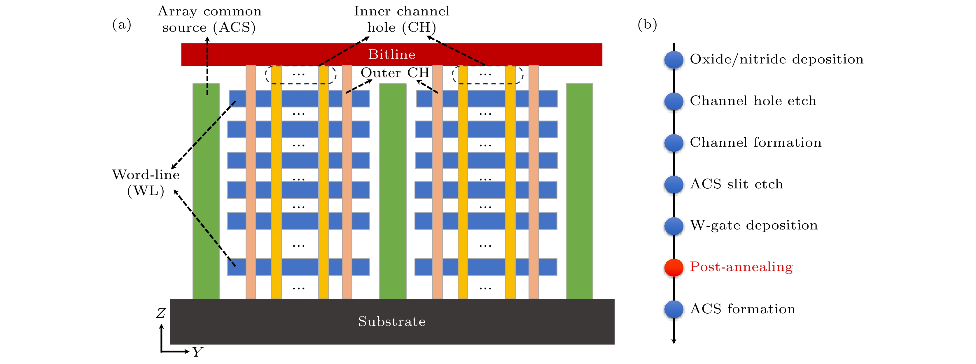
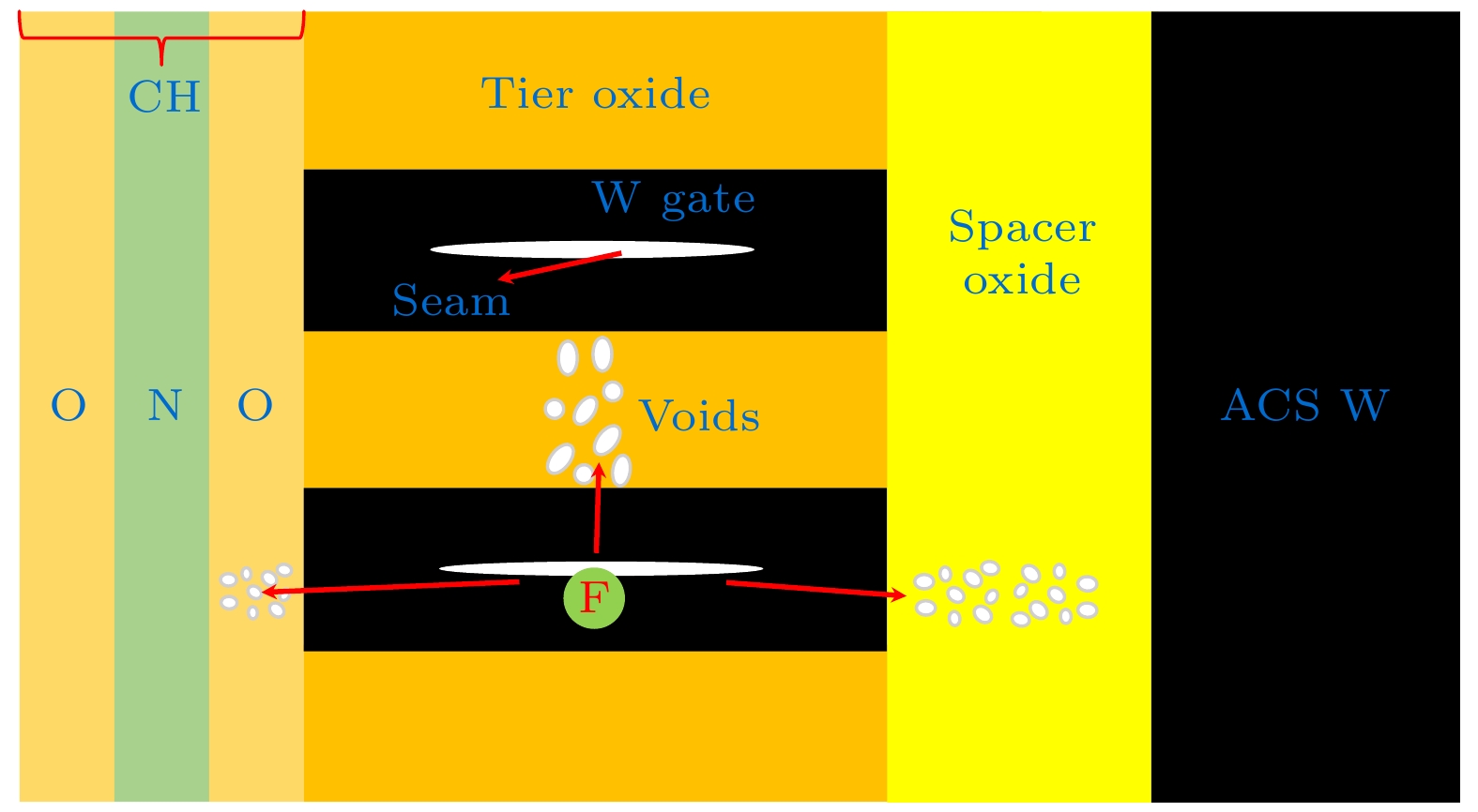
图 2 (a) Y-Z 方向的3D NAND阵列结构示意图; (b) 3D NAND阵列的制造工艺流程(外排孔靠近阵列公共源区, 内排孔远离阵列公共源区)
Figure 2. (a) Schematic diagram of the 3D NAND array structure in the Y-Z direction; (b) the manufacturing process of 3D NAND array (the outer hole is close to the array common source area, and the inner hole is far away from the array common source area).
-
[1] Compagnoni C M, Goda A, Spinelli A S, Feeley P, Lacaita A L, Visconti A 2017 Proc. IEEE 105 1609
 Google Scholar
[2] Kim H, Ahn S J, Shin Y G, Lee K, Jung E 2017 IEEE International Memory Workshop (IMW) Monterey, California, May 14–17, 2017 p1
[3] Vasilyev V, Chung S H, Song Y W 2007 Solid State Technol. 50 53
[4] Xu Q, Luo J, Wang G, Yang T, Li J, Ye T, Chen D, Zhao C 2015 Microelectron. Eng. 137 43
 Google Scholar
[5] Moon J, Lee T Y, Ahn H J, Lee T I, Hwang W S, Cho B J 2018 IEEE Trans. Electron Dev. 66 378
 Google Scholar
[6] Bakke J, Lei Y, Xu Y, Daito K, Fu X, Jian G, Wu K, Hung R, Jakkaraju R, Breil N 2016 IEEE International Interconnect Technology Conference/Advanced Metallization Conference (IITC/AMC) San Jose, California, USA, May 23–26, 2016 p108
[7] Lee J H, Hidayat R, Ramesh R, Roh H, Nandi D K, Lee W J, Kim S H 2022 Appl. Surf. Sci. 578 152062
 Google Scholar
[8] Kim C H, Rho I C, Kim S H, Han I K, Kang H S, Ryu S W, Kim H J 2009 J. Electrochem. Soc. 156 H685
 Google Scholar
[9] Subramaniyan A, Luppi D F, Makela N, Bauer L, Madan A, Murphy R, Baumann F, Kohli K, Parks C 2016 27th Annual SEMI Advanced Semiconductor Manufacturing Conference (ASMC) Saratoga Springs, New York, USA, May 16–19, 2016 p313
[10] Song Y J, Xia Z L, Hua W Y, Liu F, Huo Z L 2018 IEEE International Conference on Integrated Circuits, Technologies and Applications (ICTA) Beijing, China, November 21–23, 2018 p120
[11] Mistry K, Allen C, Auth C, Beattie B, Bergstrom D, Bost M, Brazier M, Buehler M, Cappellani A, Chau R 2007 IEEE International Electron Devices Meeting Washington, DC, December 10–12, 2007 p247
[12] Leusink G, Oosterlaken T, Janssen G, Redelaar S 1993 Thin Solid Films 228 125
 Google Scholar
[13] Kodas T T, Hampden S M J 2008 The Chemistry of Metal CVD (John Wiley & Sons) p112
[14] Klaus J, Ferro S, George S 2000 Thin Solid Films 360 145
 Google Scholar
[15] Hidayat R, Chowdhury T, Kim Y, Kim S, Mayangsari T R, Kim S H, Lee W J 2021 Appl. Surf. Sci. 538 148156
 Google Scholar
[16] Park H, Lee S, Kim H J, Woo D, Lee J M, Yoon E, Lee G D 2018 RSC Adv. 8 39039
 Google Scholar
[17] Schulze S, Wolansky D, Katzer J, Schubert M, Costina I, Mai A 2018 IEEE Trans. Semicond. Manuf. 31 528
 Google Scholar
[18] Kalanyan B, Lemaire P C, Atanasov S E, Ritz M J, Parsons G N 2016 Chem. Mater. 28 117
 Google Scholar
[19] Lee J H, Kim H W, Park I H, Cho S, Lee G S, Kim D H, Yun J G, Kim Y, Lee J D, Park B G 2006 IEEE Nanotechnology Materials and Devices Conference New York, USA, October 22–25, 2006 p638
[20] Yang Y, Zhu H, Meng X, Jin L, Wang C, Wang S, Feng S, Guo C, Zhang Y 2018 14th IEEE International Conference on Solid-State and Integrated Circuit Technology (ICSICT) Qingdao, China, October 31–November 3, 2018 p1
Catalog
Metrics
- Abstract views: 7295
- PDF Downloads: 185
- Cited By: 0


 DownLoad:
