-
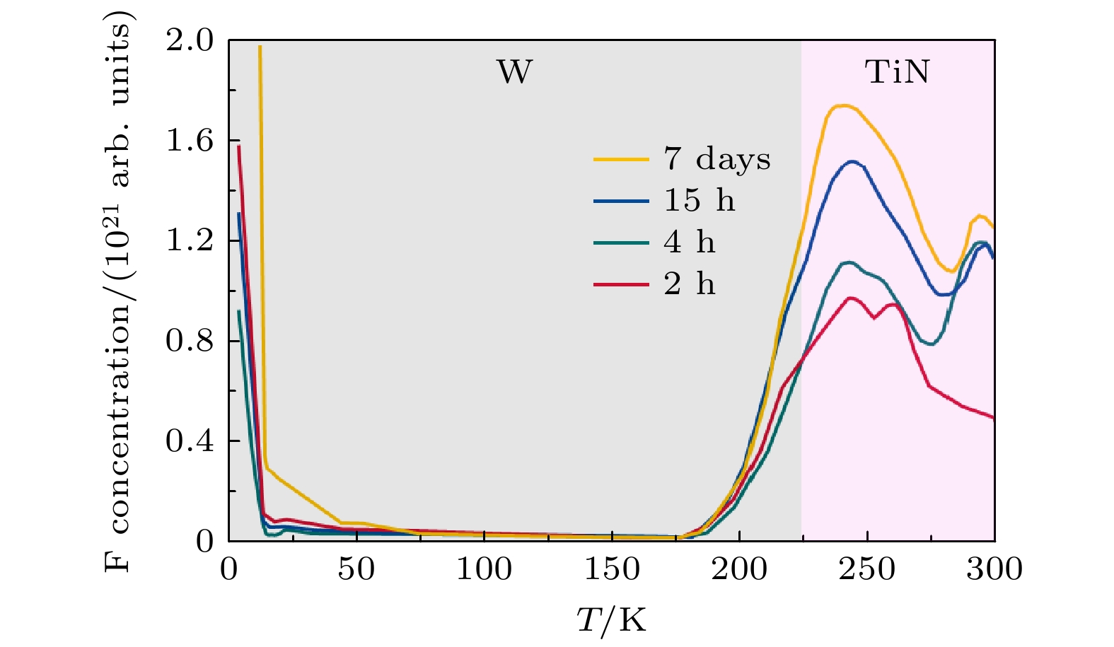
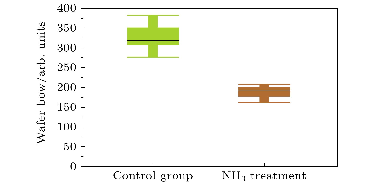
随着3D NAND技术的发展, 存储阵列工艺的堆叠层数越来越高, 后栅工艺中金属钨(W)栅字线(WL)层填充的工艺也面临越来越严峻的挑战. 钨栅沉积工艺中的主要挑战在于氟攻击问题, 钨栅填充时产生的空洞导致了含氟(F)副产物的积聚, 并在后续高温制程的激发下, 扩散侵蚀其周边氧化物层, 致使字线漏电, 严重影响器件的良率及可靠性. 为改善氟攻击问题, 通常在钨栅沉积之前再沉积一层薄的氮化钛作为阻挡层. 然而在对栅极叠层组分分析中发现, F元素聚集在TiN薄膜表面, 并且难以通过退火排出. 本文采用第一性原理计算, 研究了TiN薄膜表面吸附含F物种的情况, 提出TiN的表面氧化能加剧对含F物种的吸附作用, 仿真结果指导了栅极工艺过程的优化方向. 基于第一性原理计算结果, 提出氨气吹扫表面处理方法, 有效改善了3D NAND中的氟攻击问题, 将字线漏电率降低25%, 晶圆翘曲度降低43%.Three-dimensional (3D) NAND flash memory is a key technology in the field of mainstream memory solutions, which is primarily due to its extremely low bit cost. The architecture of 3D NAND, characterized by its vertically stacked design, substantially enhances the capacity of individual chips. This advancement is completely consistent with the demands for high-capacity data storage in contemporary environments, securing its widespread adoption in diverse application scenarios. As storage density increases, the complexity of process integration increases, bringing new challenges. The word lines in 3D NAND are typically filled by using gate replacement techniques, and compared with chemical vapor deposition (CVD), atomic layer deposition (ALD) is favored for its superior step-coverage, especially for depositing tungsten (W) at the gate. However, due to the complexity of the replacement gate deposition structure, fluorine (F) residues are found in the voids of the tungsten metal gate filling structure and diffuse into the surrounding structure under subsequent process conditions, corroding other films such as silicon oxide and degrading device performance and reliability. To alleviate the problem of fluorine attack, a thin layer of titanium nitride is usually deposited as a barrier layer before deposition of tungsten gate, which blocks the fluorine in the tungsten gate and prevents its diffusion into the oxide layer. Previously, there were studies to increase the ability to stop F diffusion by varying the thickness of the F blocking layer (TiN). However, increasing the thickness of TiN will further increase the complexity of high aspect ratio etching in the 3D NAND process, which will have adverse effect on subsequent processes. To further minimize the effect of fluorine erosion, residual fluorine elements can be removed by introducing annealing in the subsequent process flow. In the actual 3D NAND process, elemental fluorine (F) is adsorbed and accumulates on the TiN surface, and is further activated by subsequent high-temperature processes, leading to severe fluorine erosion. The delay between TiN deposition and subsequent processing steps is hypothesized to facilitate fluorine adsorption due to the oxidation of TiN. This work corroborates this hypothesis through first-principles calculations, and demonstrates the role of TiN oxidation in fluorine adsorption. In this work, we evaluate the effect of this oxidation on the fluorine-blocking effectiveness of the TiN barrier layer. We simulate the adsorption of fluorine-containing by-products on TiN and its oxides, providing theoretical insights into mitigating fluorine attack. The higher degree of oxidation of TiN is more likely to cause F adsorption, and Ti exposed surface TiN is more prone to oxidation, which is more likely to cause F adsorption in unoxidized condition and oxidized condition. Based on these insights, we implemente an ammonia purge treatment in 3D NAND manufacturing, which effectively minimizes fluorine attack, reducing the leakage probability of word line by 25% and wafer warpage by 43%.
[1] Compagnoni C M, Goda A, Spinelli A S, Feeley P, Lacaita A L, Visconti A 2017 Proc. IEEE 105 1609
 Google Scholar
[2] Vasilyev V, Chung S H, Song Y W 2007 Solid State Technol. 50 53
[3] Mistry K, Allen C, Auth C, Beattie B, Bergstrom D, Bost M, Brazier M, Buehler M, Cappellani A, Chau R 2007 IEEE International Electron Devices Meeting Washington, DC, USA, December 10–12, 2007 p247
[4] Song Y J, Xia Z L, Hua W Y, Liu F, Huo Z L 2018 IEEE International Conference on Integrated Circuits, Technologies and Applications (ICTA) Beijing, China, November 21–23, 2018 p120
[5] Schulze S, Wolansky D, Katzer J, Schubert M, Costina I, Mai A 2018 IEEE Trans. Semicond. Manuf. 31 528
 Google Scholar
[6] Bakke J, Lei Y, Xu Y, Daito K, Fu X, Jian G, Wu K, Hung R, Jakkaraju R, Breil N 2016 IEEE International Interconnect Technology Conference/Advanced Metallization Conference (IITC/AMC) San Jose, California, USA, May 23–26, 2016 p108
[7] Lee J H, Hidayat R, Ramesh R, Roh H, Nandi D K, Lee W J, Kim S H 2022 Appl. Surf. Sci. 578 152062
 Google Scholar
[8] Subramaniyan A, Luppi D F, Makela N, Bauer L, Madan A, Murphy R, Baumann F, Kohli K, Parks C 2016 27th Annual SEMI Advanced Semiconductor Manufacturing Conference (ASMC) Saratoga Springs, New York, USA, May 16–19, 2016 p313
[9] Perdew J P, Burke K, Ernzerhof M 1996 Phys. Rev. Lett. 77 3865
 Google Scholar
[10] Payne M C, Teter M P, Allan D C, Arias T, Joannopoulos A J 1992 Rev. Mod. Phys. 64 1045
 Google Scholar
[11] Blöchl P E, Kästner J, Först C J 2005 Handbook of Materials Modeling: Methods (Springer) p93
[12] Bonhomme C, Gervais C, Babonneau F, Coelho C, Pourpoint F, Azais T, Ashbrook S E, Griffin J M, Yates J R, Mauri F 2012 Chem. Rev. 112 5733
 Google Scholar
[13] Zhang W, Cai J, Wang D, Wang Q, Wang S 2010 11th International Conference on Electronic Packaging Technology & High Density Packaging (ICEPT-HDP) Xi’an, China, August 16–19, 2010 pp7–11
[14] Abrahams S, Bernstein J 1971 J. Chem. Phys. 55 3206
 Google Scholar
[15] Monkhorst H J, Pack J D 1976 Phys. Rev. B 13 5188
 Google Scholar
[16] Armstrong D, Perkins P 1969 Theor. Chim. Acta 15 413
 Google Scholar
[17] Carosati E, Sciabola S, Cruciani G 2004 J. Med. Chem. 47 5114
 Google Scholar
[18] Lennard-Jones J 1932 Trans. Faraday Soc. 28 333
 Google Scholar
[19] Perron H, Domain C, Roques J, Drot R, Simoni E, Catalette H 2007 Theor. Chem. Acc. 117 565
 Google Scholar
[20] Nilsson K B 2005 Coordination Chemistry in Liquid Ammonia and Phosphorous Donor Solvents (Department of Chemistry, Swedish University of Agricultural Sciences) p7
[21] Kuchitsu K, Konaka S 1966 J. Chem. Phys. 45 4342
 Google Scholar
[22] Jebasty R M, Vidya R 2019 ACS Biomaster Sci. Eng. 5 2001
 Google Scholar
[23] Izadi S, Anandakrishnan R, Onufriev A V 2014 J. Phys. Chem. Lett. 5 3863
 Google Scholar
-
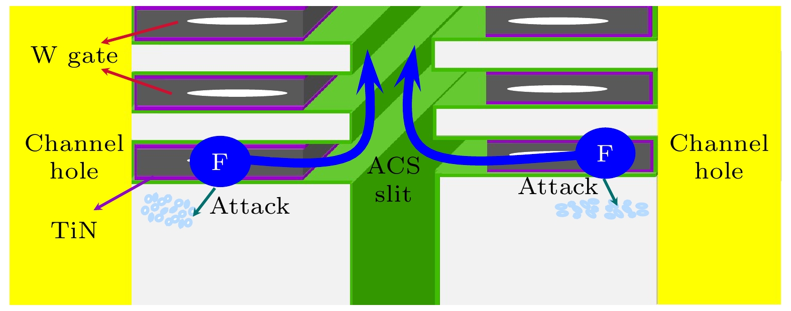
图 1 替换栅结构与氟攻击氧化物的示意图, 说明氧化物层被腐蚀的机理, 蓝色箭头表示退火后氟逸散的通道, 说明退火可以排出剩余的氟元素
Fig. 1. Schematic diagram of fluorine attacks oxide, illustrating the corrosion mechanism of the ox-ide layer in the W gate. The blue arrow indicates the channel for fluorine escape after annealing, illustrating that thermal processing can discharge the remaining F element.
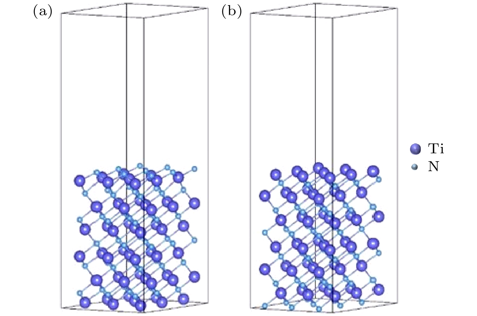
图 4 (a) TiN(111) N暴露表面吸附HF后的稳定结构; (b) TiN(111) N暴露表面吸附BF3后的稳定结构; (c) TiN(111) Ti暴露表面吸附HF后的稳定结构; (d) TiN(111) Ti暴露表面吸附BF3后的稳定结构
Fig. 4. (a) Stable structure of TiN(111) after adsorption of HF on the N exposed surface; (b) stable structure of TiN(111) after adsorption of BF3 on the N exposed surface; (c) stable structure of TiN(111) after adsorption of HF on the Ti exposed surface; (d) stable structure of TiN(111) after adsorption of BF3 on the Ti exposed surface.
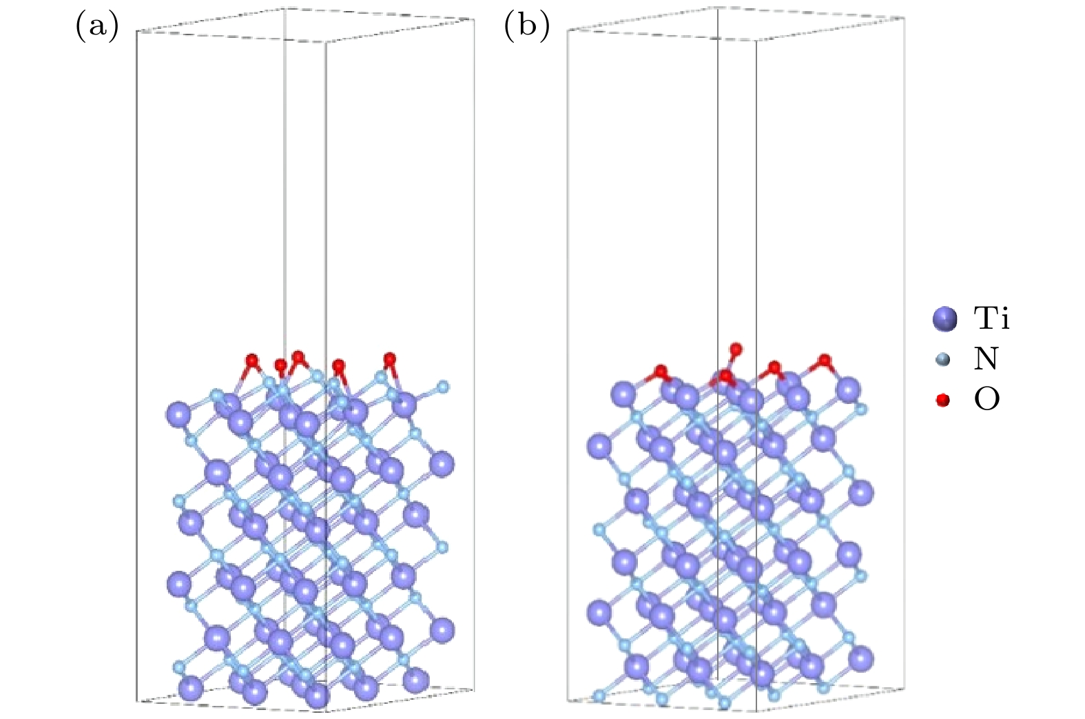
图 7 (a) N暴露表面氧化后的TiON(111)表面吸附HF后的稳定结构; (b) N暴露表面氧化后的TiON(111) 表面吸附BF3后的稳定结构; (c) Ti暴露表面氧化后的TiON(111) 表面吸附HF后的稳定结构; (d) Ti暴露表面氧化后的TiON(111) 表面吸附BF3后的稳定结构
Fig. 7. (a) Stable structure of HF adsorption on the TiON(111) surface oxidized from the N-exposed surface; (b) stable structure of BF3 adsorption on the TiON(111) surface oxidized from the N-exposed surface; (c) stable structure of HF adsorption on the TiON(111) surface oxidized from the Ti-exposed surface; (d) stable structure of BF3 adsorption on the TiON(111) surface oxidized from the Ti-exposed surface.
表 1 TiN(111) N暴露表面、TiN(111) Ti暴露表面吸附HF和BF3后的键长
Table 1. Bond lengths after HF and BF3 adsorption on the N-exposed surface of TiN(111) and the Ti-exposed surface of TiN(111).
表 2 TiO2(100) 表面吸附HF和BF3后的键长
Table 2. Bond lengths after HF and BF3 adsorption on the TiO2(100) surface.
吸附表面 吸附分子 成键类型 键长/Å 理想键长/Å 吸附能/eV TiO2(100) HF Ti—F 1.83 1.74(TiF4) –1.92 O—H 0.97 0.96(H2O)[23] TiO2(100) BF3 Ti—F 2.10 1.74(TiF4) –1.98 B—F 1.48 1.31(BF3) 表 3 TiON(111) N暴露表面、TiON(111) Ti暴露表面吸附HF和BF3后的键长
Table 3. Bond lengths after HF and BF3 adsorption on the N-exposed surface of TiON(111) and the Ti-exposed surface of TiON(111).
吸附表面 吸附分子 成键类型 键长/Å 理想键长/Å 吸附能/eV N-TiON(111) HF O—H 1.86 0.96(H2O) –0.23 BF3 B—F 1.32 1.31(BF3) –0.06 Ti-TiON(111) HF O—H 0.97 0.96(H2O) –2.28 Ti—F 2.18 1.74(TiF4) BF3 Ti—F 2.18 1.74(TiF4) –1.40 B—F 1.33 1.31(BF3) -
[1] Compagnoni C M, Goda A, Spinelli A S, Feeley P, Lacaita A L, Visconti A 2017 Proc. IEEE 105 1609
 Google Scholar
[2] Vasilyev V, Chung S H, Song Y W 2007 Solid State Technol. 50 53
[3] Mistry K, Allen C, Auth C, Beattie B, Bergstrom D, Bost M, Brazier M, Buehler M, Cappellani A, Chau R 2007 IEEE International Electron Devices Meeting Washington, DC, USA, December 10–12, 2007 p247
[4] Song Y J, Xia Z L, Hua W Y, Liu F, Huo Z L 2018 IEEE International Conference on Integrated Circuits, Technologies and Applications (ICTA) Beijing, China, November 21–23, 2018 p120
[5] Schulze S, Wolansky D, Katzer J, Schubert M, Costina I, Mai A 2018 IEEE Trans. Semicond. Manuf. 31 528
 Google Scholar
[6] Bakke J, Lei Y, Xu Y, Daito K, Fu X, Jian G, Wu K, Hung R, Jakkaraju R, Breil N 2016 IEEE International Interconnect Technology Conference/Advanced Metallization Conference (IITC/AMC) San Jose, California, USA, May 23–26, 2016 p108
[7] Lee J H, Hidayat R, Ramesh R, Roh H, Nandi D K, Lee W J, Kim S H 2022 Appl. Surf. Sci. 578 152062
 Google Scholar
[8] Subramaniyan A, Luppi D F, Makela N, Bauer L, Madan A, Murphy R, Baumann F, Kohli K, Parks C 2016 27th Annual SEMI Advanced Semiconductor Manufacturing Conference (ASMC) Saratoga Springs, New York, USA, May 16–19, 2016 p313
[9] Perdew J P, Burke K, Ernzerhof M 1996 Phys. Rev. Lett. 77 3865
 Google Scholar
[10] Payne M C, Teter M P, Allan D C, Arias T, Joannopoulos A J 1992 Rev. Mod. Phys. 64 1045
 Google Scholar
[11] Blöchl P E, Kästner J, Först C J 2005 Handbook of Materials Modeling: Methods (Springer) p93
[12] Bonhomme C, Gervais C, Babonneau F, Coelho C, Pourpoint F, Azais T, Ashbrook S E, Griffin J M, Yates J R, Mauri F 2012 Chem. Rev. 112 5733
 Google Scholar
[13] Zhang W, Cai J, Wang D, Wang Q, Wang S 2010 11th International Conference on Electronic Packaging Technology & High Density Packaging (ICEPT-HDP) Xi’an, China, August 16–19, 2010 pp7–11
[14] Abrahams S, Bernstein J 1971 J. Chem. Phys. 55 3206
 Google Scholar
[15] Monkhorst H J, Pack J D 1976 Phys. Rev. B 13 5188
 Google Scholar
[16] Armstrong D, Perkins P 1969 Theor. Chim. Acta 15 413
 Google Scholar
[17] Carosati E, Sciabola S, Cruciani G 2004 J. Med. Chem. 47 5114
 Google Scholar
[18] Lennard-Jones J 1932 Trans. Faraday Soc. 28 333
 Google Scholar
[19] Perron H, Domain C, Roques J, Drot R, Simoni E, Catalette H 2007 Theor. Chem. Acc. 117 565
 Google Scholar
[20] Nilsson K B 2005 Coordination Chemistry in Liquid Ammonia and Phosphorous Donor Solvents (Department of Chemistry, Swedish University of Agricultural Sciences) p7
[21] Kuchitsu K, Konaka S 1966 J. Chem. Phys. 45 4342
 Google Scholar
[22] Jebasty R M, Vidya R 2019 ACS Biomaster Sci. Eng. 5 2001
 Google Scholar
[23] Izadi S, Anandakrishnan R, Onufriev A V 2014 J. Phys. Chem. Lett. 5 3863
 Google Scholar
计量
- 文章访问数: 3372
- PDF下载量: 230
- 被引次数: 0


 下载:
下载:
