-
Spintronics is a new type of electronics based on electron spin rather than charge as the information carrier, which can be stored and calculated by regulating and manipulating the spin. The discovery and application of the giant magnetoresistance effect opens the door to the application of electron spin properties. Realizing on-demand control of spin degree of freedom for spin-based devices is essential. The two-dimensional novel material, monolayer transition metal dichalcogenide (TMD) (MoS2 is a typical example from the family of TMD materials), has become an excellent platform for studying spintronics due to its novel physical properties, such as direct band gap and strong spin-orbit coupling. Obtaining high spin polarization and achieving controllability of degrees of freedom are fundamental problems in spintronics. In this paper, we construct the monolayer zigzag MoS2 nanoribbon quantum structure of electrically controlled ferromagnetic electrode to solve this problem. Based on the non-equilibrium Green’s function method, the regulation of the magnetic exchange field and electrostatic barrier on the spin transport in parallel configuration and anti-parallel configuration are studied. It is found that in the parallel structure, spin transport is obviously related to the magnetic exchange field, and 100% spin filtering can occur near the Fermi energy level to obtain pure spin current. When an additional electric field is applied to the middle region, the spin filtering effect is more significant. Therefore, the spin switching effect can be achieved by regulating the incident energy. In addition, it is also found that within a specific energy range, electrons in the parallel configuration are excited to participate in transport, while electrons in the anti-parallel structure are significantly inhibited. Consequently, a noticeable giant magnetoresistance effect can be obtained in this quantum structure. Moreover, it can be seen that the magnetic exchange field strength can effectively modulate the giant magnetoresistance effect. These results provide valuable theoretical references for the development of giant magnetoresistance devices and spin filters based on monolayer zigzag MoS2 nanoribbons.
-
Keywords:
- monolayer zigzag MoS2 nanoribbon /
- magnetic exchange field /
- electric field /
- spin transport /
- giant magnetoresistance effect
[1] Mak K F, Lee C, Hone J, Heinz T F 2010 Phys. Rev. Lett. 105 136805
 Google Scholar
[2] Lu H Z, Yao W, Xiao D, Shen S Q 2013 Phys. Rev. Lett. 110 016806
 Google Scholar
[3] Xiao D, Liu G B, Feng W X, Xu X D, Yao W 2012 Phys. Rev. Lett. 108 196802
 Google Scholar
[4] Zhu Z Y, Cheng Y C, Schwingenschlögl U 2011 Phys. Rev. B 84 153402
 Google Scholar
[5] Radisavlj eVic B, Radenovic A, Brivio J, Giacometti V, Kis A 2011 Nat. Nanotechnol. 6 147
 Google Scholar
[6] Lopez-Sanchez O, Lembke D, Kayci M, Radenovic A, Kis A 2013 Nat. Nanotechnol. 8 497
 Google Scholar
[7] Rahimi F, Phirouznia A 2022 Sci. Rep. 12 7800
 Google Scholar
[8] Liu G B, Shan W Y, Yao Y, Yao W, Xiao D 2013 Phys. Rev. B 88 085433
 Google Scholar
[9] Baibich M N, Broto J M, Fert A, Nguyen V D F, Petroff F, Etienne P, Creuzet G, Friederich A, Chazelas J 1988 Phys. Rev. Lett. 61 2472
 Google Scholar
[10] Thompson S M 2008 Appl. Phys. 41 093001
 Google Scholar
[11] Prinz G A 1998 Science 282 1660
 Google Scholar
[12] Binasch G, Grünberg P, Saurenbach F, Zinn W 1989 Phys. Rev. B 39 4828
 Google Scholar
[13] Zhang X L, Gong P W, Liu F Q, Yao K L, Wu J, Zhu S C 2022 Front. Phys 17 53510
 Google Scholar
[14] Pan H, Zhang Y W 2012 J. Mater. Chem. 22 7280
 Google Scholar
[15] Botello-Méndez A R, López-Urías F, Terrones M, Terrones H 2009 Nanotechnology 20 325703
 Google Scholar
[16] Tong X, Ashalley E, Lin F, Li H, Wang Z M 2015 Nano-Micro. lett. 7 203
 Google Scholar
[17] Backman J, Lee Y, Luisier M 2022 Solid State Electron. 35 8092
[18] Song J F, Qi Y B, Xiao Z Y, Wang K, Li D W, Kim S H, Kingon A I, Rappe A M, Hong X 2019 NPJ 2D Mater. Appl. 6 77
 Google Scholar
[19] Lembke D, Kis A 2013 ACS Nano 7 3730
 Google Scholar
[20] 张理勇, 方粮, 彭向阳 2016 65 127101
 Google Scholar
Zhang L Y, Fang L, Peng X Y 2016 Acta Phys. Sin. 65 127101
 Google Scholar
[21] 董海明 2013 62 206101
 Google Scholar
Dong H M 2013 Acta Phys. Sin. 62 206101
 Google Scholar
[22] Rachel S, Ezawa M 2014 Phys. Rev. B 89 195303
 Google Scholar
[23] Li H, Shao J M, Yao D X, Yang G W 2014 ACS Appl. Mater. Interfaces 6 1759
 Google Scholar
[24] Zheng J, Xiang Y, Li C L, Yuan R Y, Chi F, Guo Y 2020 Phys. Rev. Applied 14 034027
 Google Scholar
[25] Lu W T, Sun Q F, Li Y F, Tian H Y 2021 Phys. Rev. B 104 195419
 Google Scholar
[26] You S, Park D, Kim H, Kim N 2022 Curr. Appl. Phys. 37 52
 Google Scholar
[27] Li F, Zhang Q T 2022 Micro. Nanostruct. 163 107129
 Google Scholar
[28] Li Y, Jiang W Q, Ding G Y, Peng Y Z, Wen Z C, Wang G Q, Bai R, Qian Z H, Xiao X B, Zhou G H 2019 J. Appl. Phys. 125 244304
 Google Scholar
[29] Srivastava A, Sidler M, Allain A V, Lembke D S, Kis A, Imamoğlu A 2015 Nature Nanotech. 10 491
 Google Scholar
[30] Srivastava A, Sidler M, Allain A V, Lembke D S, Kis A, Imamoğlu A 2015 Nature Phys. 11 141
 Google Scholar
-
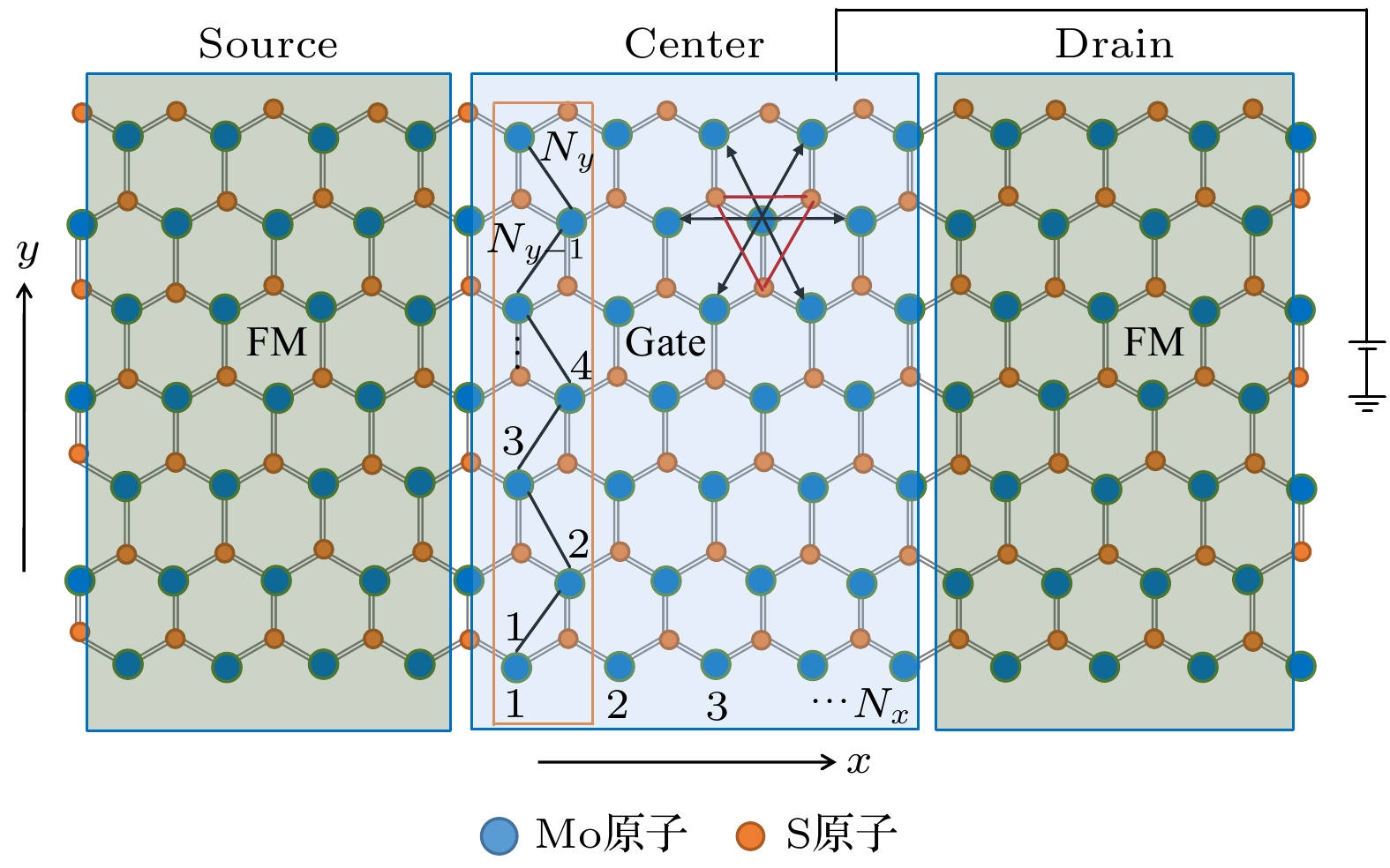
图 1 铁磁电极单层二硫化钼纳米带量子结构模型示意图. 桔色矩形区域表示元胞; 中间区域长度, 即元胞个数为
$ {N}_{x} $ ; 纳米带宽度, 既Mo原子层数为$ {N}_{y} $ Figure 1. Quantum structure model of monolayer MoS2 nanoribbons with ferromagnetic (FM) electrodes. The cell is represented by the orange rectangle. The length of the middle region, i.e., the number of cells is
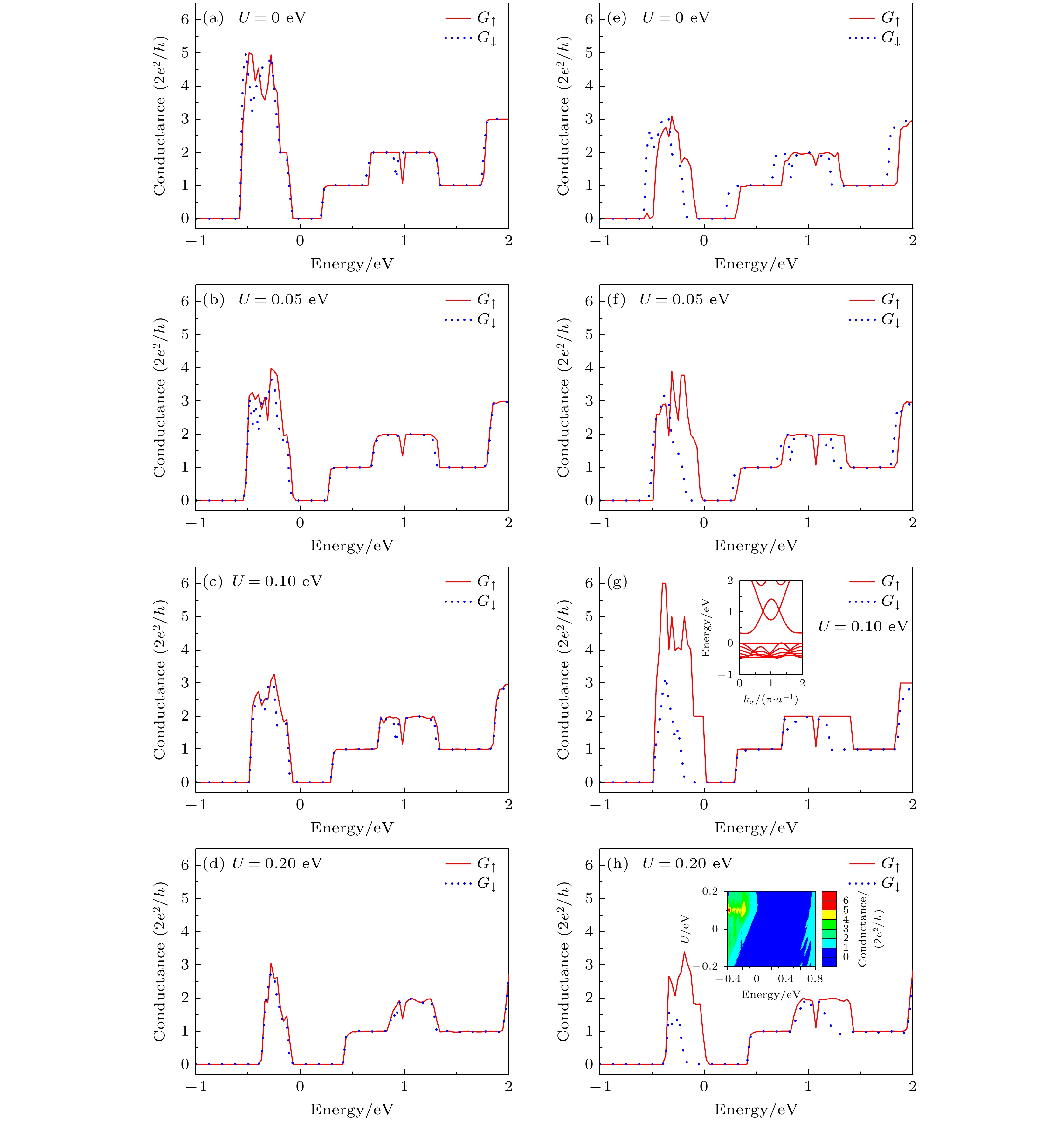
$ {N}_{x} $ ; nanoribbon width, i.e., Mo atomic layer number is$ {N}_{y} $ .图 2 磁交换场强度(M)不变, 中间区域施加不同强度电场(U)时, 自旋电导随入射能量变化的曲线图 (a)−(d)
$ M=0.01 $ eV; (e)−(h)$ M=0.1 $ eV, (h)中插图为上自旋电导随不同入射能、中间区域电势能变化的等高线图, (g)中插图为上自旋电子的能带图. 其他参数为中间区域长度${N_x} = 14$ , 纳米带宽度${N_y} = 8$ Figure 2. Spin conductance as a function of incident energy with several electric fields applied in the middle region for the magnetic exchange field of (a)−(d)
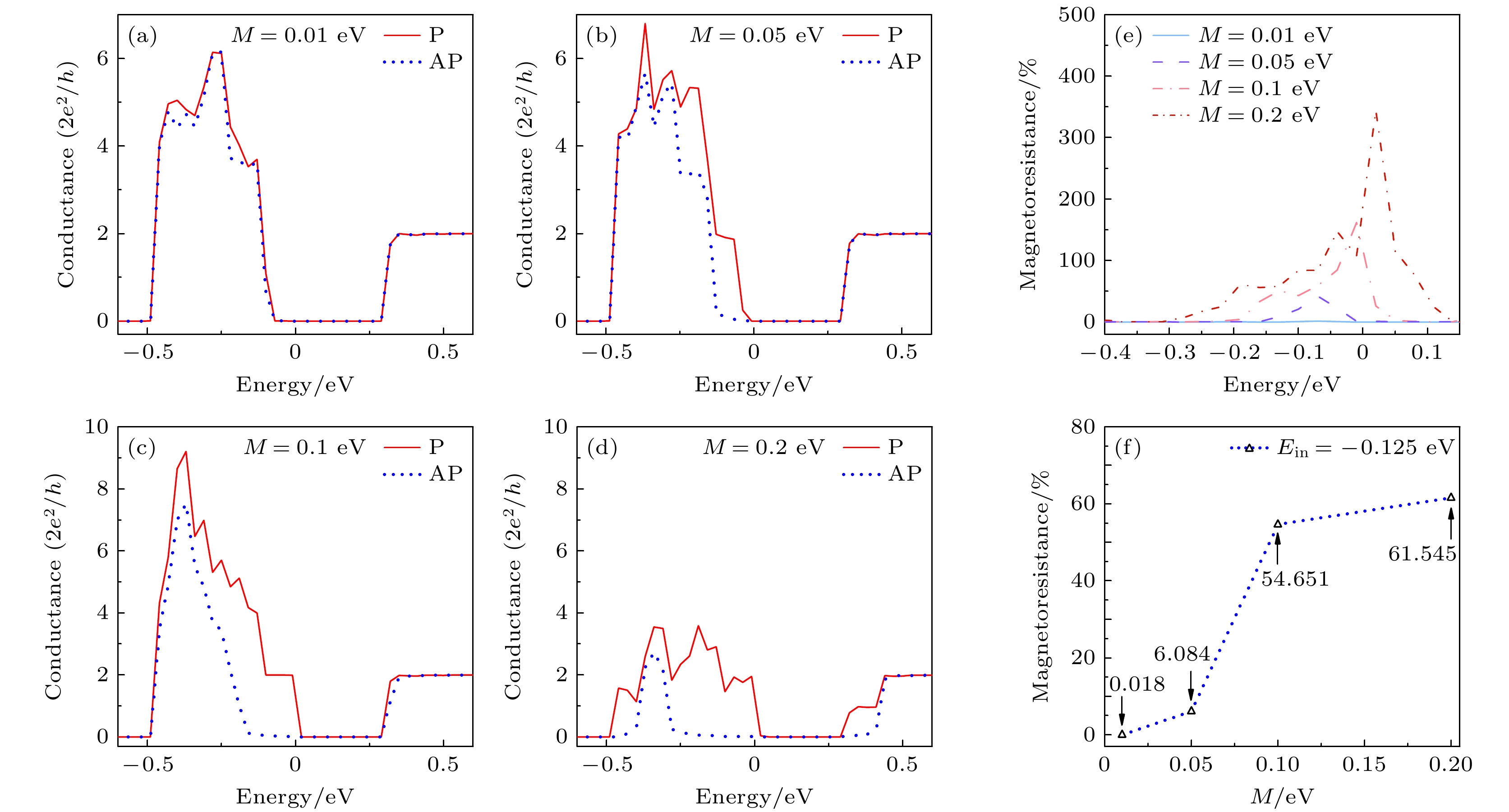
$ M=0.01\;\text{eV} $ and (e)−(h)$ M=0.1\;\text{eV} $ . The insert in (h) shows the contour diagram of spin-up conductance with different incident energies and potential energies in the middle region. The insert in (g) shows the energy-band diagram of spin-up electrons. The other parameters are${N_x} = 14$ ,${N_y} = 8$ .图 4 (a)−(d) 不同磁化强度下, 磁化方向平行和反平行时电导随入射能的变化曲线图; (e)磁阻率随入射能变化的曲线图; (f)磁阻率随磁交换场强度变化的趋势图, 入射能
${E_{{\text{in}}}} = - 0.125$ eV. 其他参数为中间区域长度${N_x} = 14$ , 纳米带宽度${N_y} = 8$ , 中间区域电势能$U = 0.1$ eVFigure 4. (a)−(d) Spin conductance as a function of the incident energy when the magnetization directions are parallel and anti-parallel with different magnetization intensities; (e) the magnetoresistance as a function of the incident energy; (f) the magnetoresistance as a function of the magnetic exchange field intensity, where the incident energy is
${E_{{\text{in}}}} = - 0.125$ eV. The other parameters are${N_x} = 14$ ,${N_y} = 8$ , and$U = 0.1$ eV.图 5 (a)磁阻率随入射能变化的曲线图; (b)磁阻率随电场强度变化的趋势图, 入射能
${E_{{\text{in}}}} = - 0.125$ eV. 其他参数为中间区域长度${N_x} = 14$ , 纳米带宽度${N_y} = 8$ , 磁交换场强度$M = 0.1$ eVFigure 5. (a) Magnetoresistance as a function of the incident energy; (b) the magnetoresistance as a function of the electric field intensity, where the incident energy is
${E_{{\text{in}}}} = - 0.125$ eV. The other parameters are${N_x} = 14$ ,${N_y} = 8$ , and$M = 0.1$ eV.表 1 参数
$ {\varepsilon _1}, {\varepsilon _2}, {t_0}, {t_1}, {t_2}, {t_{11}}, {t_{12}}, {t_{22}}, {\lambda _{{\text{so}}}} $ 取值 (单位: eV)[8]Table 1. Values of parameter
$ {\varepsilon _1}, {\varepsilon _2}, {t_0}, {t_1}, {t_2}, {t_{11}}, {t_{12}}, {t_{22}}, {\lambda _{{\text{so}}}} $ (unit: eV)[8].$ {\varepsilon }_{1} $ $ {\varepsilon }_{2} $ $ {t}_{0} $ $ {t}_{1} $ $ {t}_{2} $ $ {t}_{11} $ $ {t}_{12} $ $ {t}_{22} $ $ {\lambda _{{\text{so}}}} $ 1.046 2.104 –0.184 0.401 0.507 0.218 0.338 0.057 0.073 -
[1] Mak K F, Lee C, Hone J, Heinz T F 2010 Phys. Rev. Lett. 105 136805
 Google Scholar
[2] Lu H Z, Yao W, Xiao D, Shen S Q 2013 Phys. Rev. Lett. 110 016806
 Google Scholar
[3] Xiao D, Liu G B, Feng W X, Xu X D, Yao W 2012 Phys. Rev. Lett. 108 196802
 Google Scholar
[4] Zhu Z Y, Cheng Y C, Schwingenschlögl U 2011 Phys. Rev. B 84 153402
 Google Scholar
[5] Radisavlj eVic B, Radenovic A, Brivio J, Giacometti V, Kis A 2011 Nat. Nanotechnol. 6 147
 Google Scholar
[6] Lopez-Sanchez O, Lembke D, Kayci M, Radenovic A, Kis A 2013 Nat. Nanotechnol. 8 497
 Google Scholar
[7] Rahimi F, Phirouznia A 2022 Sci. Rep. 12 7800
 Google Scholar
[8] Liu G B, Shan W Y, Yao Y, Yao W, Xiao D 2013 Phys. Rev. B 88 085433
 Google Scholar
[9] Baibich M N, Broto J M, Fert A, Nguyen V D F, Petroff F, Etienne P, Creuzet G, Friederich A, Chazelas J 1988 Phys. Rev. Lett. 61 2472
 Google Scholar
[10] Thompson S M 2008 Appl. Phys. 41 093001
 Google Scholar
[11] Prinz G A 1998 Science 282 1660
 Google Scholar
[12] Binasch G, Grünberg P, Saurenbach F, Zinn W 1989 Phys. Rev. B 39 4828
 Google Scholar
[13] Zhang X L, Gong P W, Liu F Q, Yao K L, Wu J, Zhu S C 2022 Front. Phys 17 53510
 Google Scholar
[14] Pan H, Zhang Y W 2012 J. Mater. Chem. 22 7280
 Google Scholar
[15] Botello-Méndez A R, López-Urías F, Terrones M, Terrones H 2009 Nanotechnology 20 325703
 Google Scholar
[16] Tong X, Ashalley E, Lin F, Li H, Wang Z M 2015 Nano-Micro. lett. 7 203
 Google Scholar
[17] Backman J, Lee Y, Luisier M 2022 Solid State Electron. 35 8092
[18] Song J F, Qi Y B, Xiao Z Y, Wang K, Li D W, Kim S H, Kingon A I, Rappe A M, Hong X 2019 NPJ 2D Mater. Appl. 6 77
 Google Scholar
[19] Lembke D, Kis A 2013 ACS Nano 7 3730
 Google Scholar
[20] 张理勇, 方粮, 彭向阳 2016 65 127101
 Google Scholar
Zhang L Y, Fang L, Peng X Y 2016 Acta Phys. Sin. 65 127101
 Google Scholar
[21] 董海明 2013 62 206101
 Google Scholar
Dong H M 2013 Acta Phys. Sin. 62 206101
 Google Scholar
[22] Rachel S, Ezawa M 2014 Phys. Rev. B 89 195303
 Google Scholar
[23] Li H, Shao J M, Yao D X, Yang G W 2014 ACS Appl. Mater. Interfaces 6 1759
 Google Scholar
[24] Zheng J, Xiang Y, Li C L, Yuan R Y, Chi F, Guo Y 2020 Phys. Rev. Applied 14 034027
 Google Scholar
[25] Lu W T, Sun Q F, Li Y F, Tian H Y 2021 Phys. Rev. B 104 195419
 Google Scholar
[26] You S, Park D, Kim H, Kim N 2022 Curr. Appl. Phys. 37 52
 Google Scholar
[27] Li F, Zhang Q T 2022 Micro. Nanostruct. 163 107129
 Google Scholar
[28] Li Y, Jiang W Q, Ding G Y, Peng Y Z, Wen Z C, Wang G Q, Bai R, Qian Z H, Xiao X B, Zhou G H 2019 J. Appl. Phys. 125 244304
 Google Scholar
[29] Srivastava A, Sidler M, Allain A V, Lembke D S, Kis A, Imamoğlu A 2015 Nature Nanotech. 10 491
 Google Scholar
[30] Srivastava A, Sidler M, Allain A V, Lembke D S, Kis A, Imamoğlu A 2015 Nature Phys. 11 141
 Google Scholar
Catalog
Metrics
- Abstract views: 5041
- PDF Downloads: 80
- Cited By: 0


 DownLoad:


