-
In order to continue Moore’s law, the reduction of power consumption has received much attention. It is necessary to develop steep devices that can overcome the “Boltzmann tyranny” and solve the problem of high power consumption of integrated circuits. Negative capacitance field-effect transistors are one of the most promising candidates in numerous steep devices. Strain engineering has been widely studied as an effective means of regulating the properties of ferroelectric thin films. However, the influence of strain on the performance of negative capacitance field-effect transistor has not been clear so far. Therefore, in this work, an analytical model of double gate negative capacitance field-effect transistor (DG-NCFET) regulated by biaxial misfit strain is proposed. Using this model, we investigate the influences of ferroelectric layer thickness and biaxial misfit strain on electrical properties of PbZr0.5Ti0.5O3 (PZT)-based and CuInP2S6 (CIPS)-based negative capacitance field-effect transistors (NCFETs), respectively. The results show that for the negative capacitance field-effect transistor based on PbZr0.5Ti0.5O3, when the ferroelectric layer thickness is increased or the compression strain is applied, the subthreshold swing and conduction current are improved, but the tensile strain has the opposite effect. For the negative capacitance field-effect transistor based on CuInP2S6, its performance is improved when the thickness of the ferroelectric layer is increased or the tensile strain is applied, but the device lags behind under the compressive strain. It is found that the CIPS-based NCFET exhibits better performance than PZT-based NCFET at low gate voltages.
[1] Danowitz A, Kelley K, Mao J, Stevenson J P, Horowitz M 2012 Commun. ACM 55 55
 Google Scholar
[2] Sakurai T 2004 IEICE Trans. Electron. 87 429
 Google Scholar
[3] Salahuddin S, Datta S 2008 Nano Lett. 8 405
 Google Scholar
[4] Tu L, Wang X, Wang J, Meng X, Chu J 2018 Adv. Electron. Mater. 4 1800231
 Google Scholar
[5] Bacharach J, Ullah M S, Fouad E 2019 IEEE 62nd International Midwest Symposium on Circuits and Systems (MWSCAS) Dallas, TX, USA, August 4–7, 2019 p180
[6] Sakib F I, Mullick F E, Shahnewaz S, Islam S, Hossain M 2020 Semicond. Sci. Technol. 35 025005
 Google Scholar
[7] 陈俊东, 韩伟华, 杨冲, 赵晓松, 郭仰岩, 张晓迪, 杨富华 2020 69 137701
 Google Scholar
Chen J D, Han W H, Yang C, Zhao X S, Guo Y Y, Zhang X D, Yang F H 2020 Acta Phys. Sin. 69 137701
 Google Scholar
[8] Lee H, Yoon Y, Shin C 2017 IEEE Electron Device Lett. 38 669
 Google Scholar
[9] Peng Y, Han G, Chen Z, Li Q, Zhang J, Hao Y 2018 IEEE J. Electron Device Soc. 6 233
 Google Scholar
[10] Jiang C, Liang R, Wang J, Xu J 2015 J. Phys. D:Appl. Phys. 48 365103
 Google Scholar
[11] Gaidhane A D, Pahwa G, Verma A, Chauhan Y S 2018 4th IEEE International Conference on Emerging Electronics (ICEE) Bengaluru, India, December 17–19, 2018 p1
[12] Choi K J, Biegalski M, Li Y L, Sharan A, Schubert J, Uecker R, Reiche P, Chen Y B, Pan X Q, Gopalan V, Chen L Q, Schlom D G, Eom C B 2004 Science 306 1005
 Google Scholar
[13] Zhang S R, Zhu M X, Suriyaprakash J, Liu J M, Du T, Wang Y J, Long C B, Liao M 2022 J. Phys. Chem. C 126 4630
 Google Scholar
[14] Haeni J, Irvin P, Chang W, Uecker R, Reiche P, Li Y, Choudhury S, Tian W, Hawley M, Craigo B 2004 Nature 430 758
 Google Scholar
[15] Schlom D G, Chen L Q, Eom C B, Rabe K M, Streiffer S K, Triscone J M 2007 Annu. Rev. Mater. Res. 37 589
 Google Scholar
[16] Sun F, Chen D, Gao X, Liu J M 2021 J. Materiomics 7 281
 Google Scholar
[17] Pertsev N A, Kukhar V G, Kohlstedt H, Waser R 2003 Phys. Rev. B 67 054107
 Google Scholar
[18] 林翠, 白刚, 李卫, 高存法 2021 70 187701
 Google Scholar
Lin C, Bai G, Li W, Gao C F 2021 Acta Phys. Sin. 70 187701
 Google Scholar
[19] Kim M, Seo J, Shin M 2018 International Conference on Simulation of Semiconductor Processes and Devices (SISPAD) Austin, TX, USA, September 24–26, 2018 p318
[20] Liu F C, You L, Seyler K L, Li X B, Yu P, Lin J H, Wang X W, Zhou J D, Wang H, He H Y, Pantelides S T, Zhou W, Sharam P, Xu X D, Ajayan P M, Wang J L, Liu Z 2016 Nat. Commun. 7 12357
 Google Scholar
[21] Morozovska A N, Eliseev E A, Kalinin S V, Vysochanskii Y M, Maksymovych P 2021 Phys. Rev. B 104 054102
 Google Scholar
[22] Wu M, Jena P 2018 Wiley Interdiscip. Rev. Comput. Mol. Sci. 8 e1365
 Google Scholar
[23] Synopsys 2010 Sentaurus Device User Guide (Mountain View, CA)
[24] Landau L, Khalatnikov I 1954 Dokl. Akad. Nauk 96 469
 Google Scholar
[25] Rabe K M, Dawber M, Lichtensteiger C, Ahn C H, Triscone J M (Rabe K M, et al. Ed. ) 2007 Physics of Ferroelectrics: A Modern Perspective (Berlin: Springer) pp1–30
[26] Pao H C, Sah C T 1966 Solid State Electron. 9 927
 Google Scholar
[27] Hoffmann M, Fengler F P G, Herzig M, Mittmann T, Max B, Schroeder U, Negrea R, Pintilie L, Slesazeck S, Mikolajick T 2019 Nature 565 464
 Google Scholar
[28] Neumayer S M, Eliseev E A, Susner M A, Tselev A, Rodriguez B J, Brehm J A, Pantelides S T, Panchapakesan G, Jesse S, Kalinin S V, McGuire M A, Morozovska A N, Maksymovych P, Balke N 2019 Phys. Rev. Mater. 3 024401
 Google Scholar
-
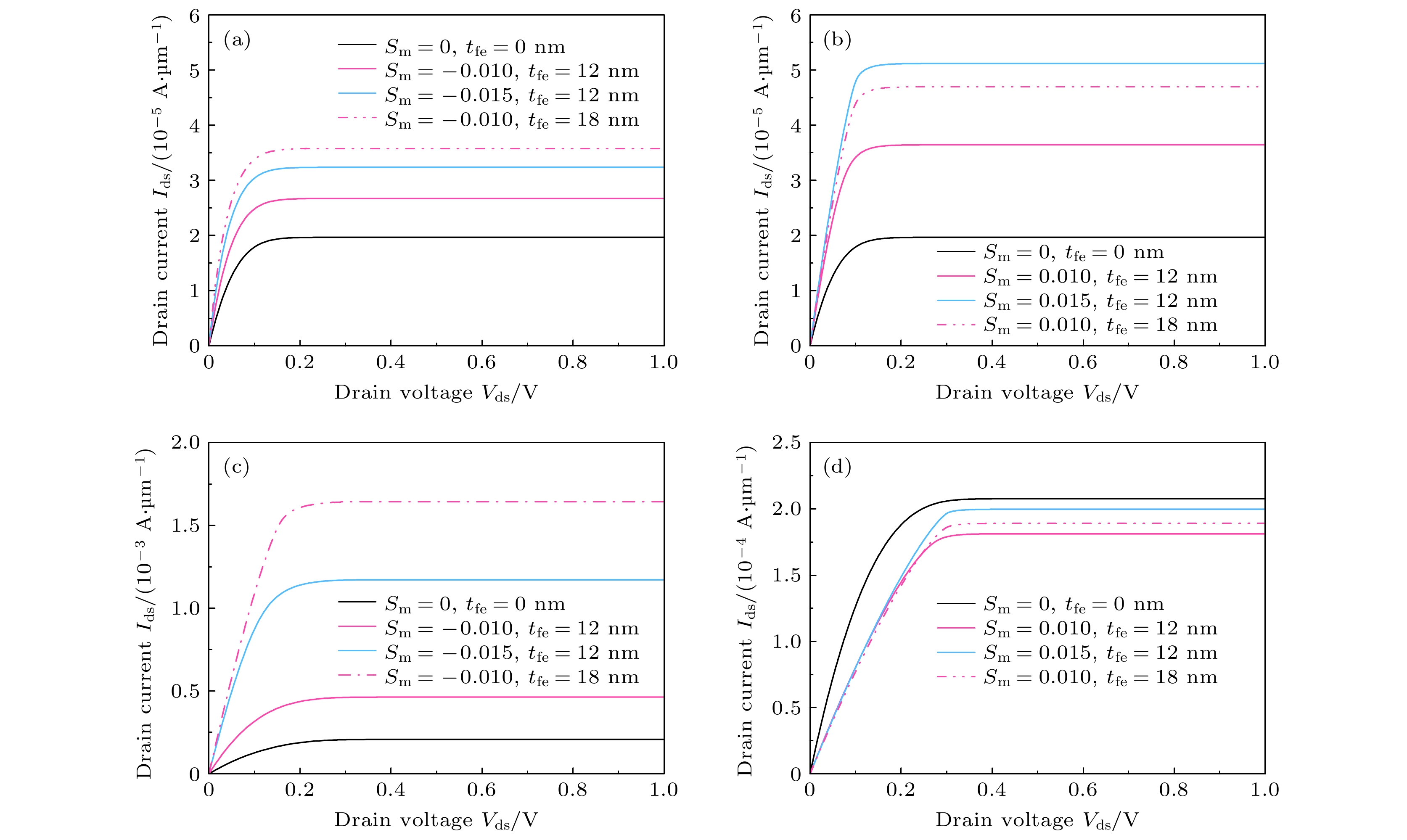
图 10 (a) Vgs = 0.6 V和(c) Vgs = 0.8 V时FE层厚度和应变对PZT基NCFET输出特性的影响; (b) Vgs = 0.6 V和(d) Vgs = 0.8 V时FE层厚度和应变对CIPS基的NCFET输出特性的影响
Figure 10. Effects of the FE layer thickness and strain on output characteristics for PZT based NCFETs at (a) Vgs = 0.6 V and (c) Vgs = 0.8 V; for CIPS based NCFETS at (b) Vgs = 0.6 V and (d) Vgs = 0.8 V.
表 1 PbZr0.2Ti0.8O3[18]和CuInP2S6[21]材料的相关系数(温度T的单位为 K)
Table 1. Paramaters for bulk ferroelectric PbZr0.2Ti0.8O3 and CuInP2S6 [18,21].
Coefficient Value PZT a1/(C–2·m2·N) 1.33(T – 665.7)×105 a11/(C–4·m6·N) 4.764×10⁷ a111/(C–4·m6·N) 1.336×10⁸ s11/(C–6·m10·N) 10.5×10⁻¹² s12/(C–6·m10·N) –3.7×10⁻¹² Q12/(m4·C–2) –0.0460 CIPS $ {\alpha }_{T}/$(C–2·mJ·K–1) 1.64067×10⁷ T0/K 292.67 α/(C–4·m5·J) 3.148×10¹² γ/(C–6·m9·J) –1.0776×10¹⁶ δ/(C–8·m13·J) 7.6318×10¹⁸ Q13/(C–2·m4) 1.70136 – 0.00363T Q23/(C–2·m4) 1.13424 – 0.00242T Q33/(C–2·m4) –5.622 + 0.0105T Z133/(C–2·m4) –2059.65 + 0.8T Z233/(C–2·m4) –1211.26 + 0.45T s11/Pa–1 1.510×10⁻¹¹ s12/Pa–1 0.183×10⁻¹¹ 结构参数 Lg/nm 1000 W/nm 1000 -
[1] Danowitz A, Kelley K, Mao J, Stevenson J P, Horowitz M 2012 Commun. ACM 55 55
 Google Scholar
[2] Sakurai T 2004 IEICE Trans. Electron. 87 429
 Google Scholar
[3] Salahuddin S, Datta S 2008 Nano Lett. 8 405
 Google Scholar
[4] Tu L, Wang X, Wang J, Meng X, Chu J 2018 Adv. Electron. Mater. 4 1800231
 Google Scholar
[5] Bacharach J, Ullah M S, Fouad E 2019 IEEE 62nd International Midwest Symposium on Circuits and Systems (MWSCAS) Dallas, TX, USA, August 4–7, 2019 p180
[6] Sakib F I, Mullick F E, Shahnewaz S, Islam S, Hossain M 2020 Semicond. Sci. Technol. 35 025005
 Google Scholar
[7] 陈俊东, 韩伟华, 杨冲, 赵晓松, 郭仰岩, 张晓迪, 杨富华 2020 69 137701
 Google Scholar
Chen J D, Han W H, Yang C, Zhao X S, Guo Y Y, Zhang X D, Yang F H 2020 Acta Phys. Sin. 69 137701
 Google Scholar
[8] Lee H, Yoon Y, Shin C 2017 IEEE Electron Device Lett. 38 669
 Google Scholar
[9] Peng Y, Han G, Chen Z, Li Q, Zhang J, Hao Y 2018 IEEE J. Electron Device Soc. 6 233
 Google Scholar
[10] Jiang C, Liang R, Wang J, Xu J 2015 J. Phys. D:Appl. Phys. 48 365103
 Google Scholar
[11] Gaidhane A D, Pahwa G, Verma A, Chauhan Y S 2018 4th IEEE International Conference on Emerging Electronics (ICEE) Bengaluru, India, December 17–19, 2018 p1
[12] Choi K J, Biegalski M, Li Y L, Sharan A, Schubert J, Uecker R, Reiche P, Chen Y B, Pan X Q, Gopalan V, Chen L Q, Schlom D G, Eom C B 2004 Science 306 1005
 Google Scholar
[13] Zhang S R, Zhu M X, Suriyaprakash J, Liu J M, Du T, Wang Y J, Long C B, Liao M 2022 J. Phys. Chem. C 126 4630
 Google Scholar
[14] Haeni J, Irvin P, Chang W, Uecker R, Reiche P, Li Y, Choudhury S, Tian W, Hawley M, Craigo B 2004 Nature 430 758
 Google Scholar
[15] Schlom D G, Chen L Q, Eom C B, Rabe K M, Streiffer S K, Triscone J M 2007 Annu. Rev. Mater. Res. 37 589
 Google Scholar
[16] Sun F, Chen D, Gao X, Liu J M 2021 J. Materiomics 7 281
 Google Scholar
[17] Pertsev N A, Kukhar V G, Kohlstedt H, Waser R 2003 Phys. Rev. B 67 054107
 Google Scholar
[18] 林翠, 白刚, 李卫, 高存法 2021 70 187701
 Google Scholar
Lin C, Bai G, Li W, Gao C F 2021 Acta Phys. Sin. 70 187701
 Google Scholar
[19] Kim M, Seo J, Shin M 2018 International Conference on Simulation of Semiconductor Processes and Devices (SISPAD) Austin, TX, USA, September 24–26, 2018 p318
[20] Liu F C, You L, Seyler K L, Li X B, Yu P, Lin J H, Wang X W, Zhou J D, Wang H, He H Y, Pantelides S T, Zhou W, Sharam P, Xu X D, Ajayan P M, Wang J L, Liu Z 2016 Nat. Commun. 7 12357
 Google Scholar
[21] Morozovska A N, Eliseev E A, Kalinin S V, Vysochanskii Y M, Maksymovych P 2021 Phys. Rev. B 104 054102
 Google Scholar
[22] Wu M, Jena P 2018 Wiley Interdiscip. Rev. Comput. Mol. Sci. 8 e1365
 Google Scholar
[23] Synopsys 2010 Sentaurus Device User Guide (Mountain View, CA)
[24] Landau L, Khalatnikov I 1954 Dokl. Akad. Nauk 96 469
 Google Scholar
[25] Rabe K M, Dawber M, Lichtensteiger C, Ahn C H, Triscone J M (Rabe K M, et al. Ed. ) 2007 Physics of Ferroelectrics: A Modern Perspective (Berlin: Springer) pp1–30
[26] Pao H C, Sah C T 1966 Solid State Electron. 9 927
 Google Scholar
[27] Hoffmann M, Fengler F P G, Herzig M, Mittmann T, Max B, Schroeder U, Negrea R, Pintilie L, Slesazeck S, Mikolajick T 2019 Nature 565 464
 Google Scholar
[28] Neumayer S M, Eliseev E A, Susner M A, Tselev A, Rodriguez B J, Brehm J A, Pantelides S T, Panchapakesan G, Jesse S, Kalinin S V, McGuire M A, Morozovska A N, Maksymovych P, Balke N 2019 Phys. Rev. Mater. 3 024401
 Google Scholar
Catalog
Metrics
- Abstract views: 5073
- PDF Downloads: 80
- Cited By: 0


 DownLoad:


