-
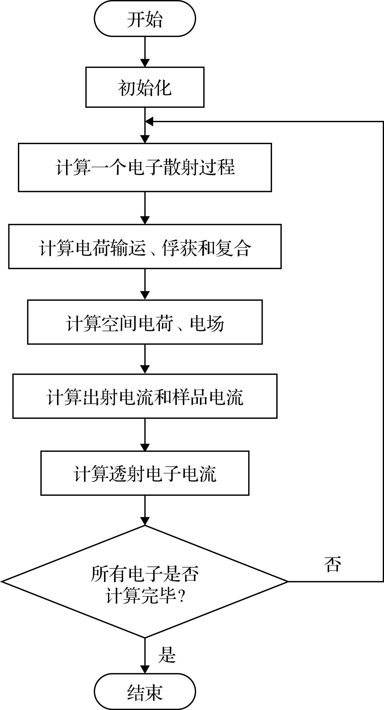
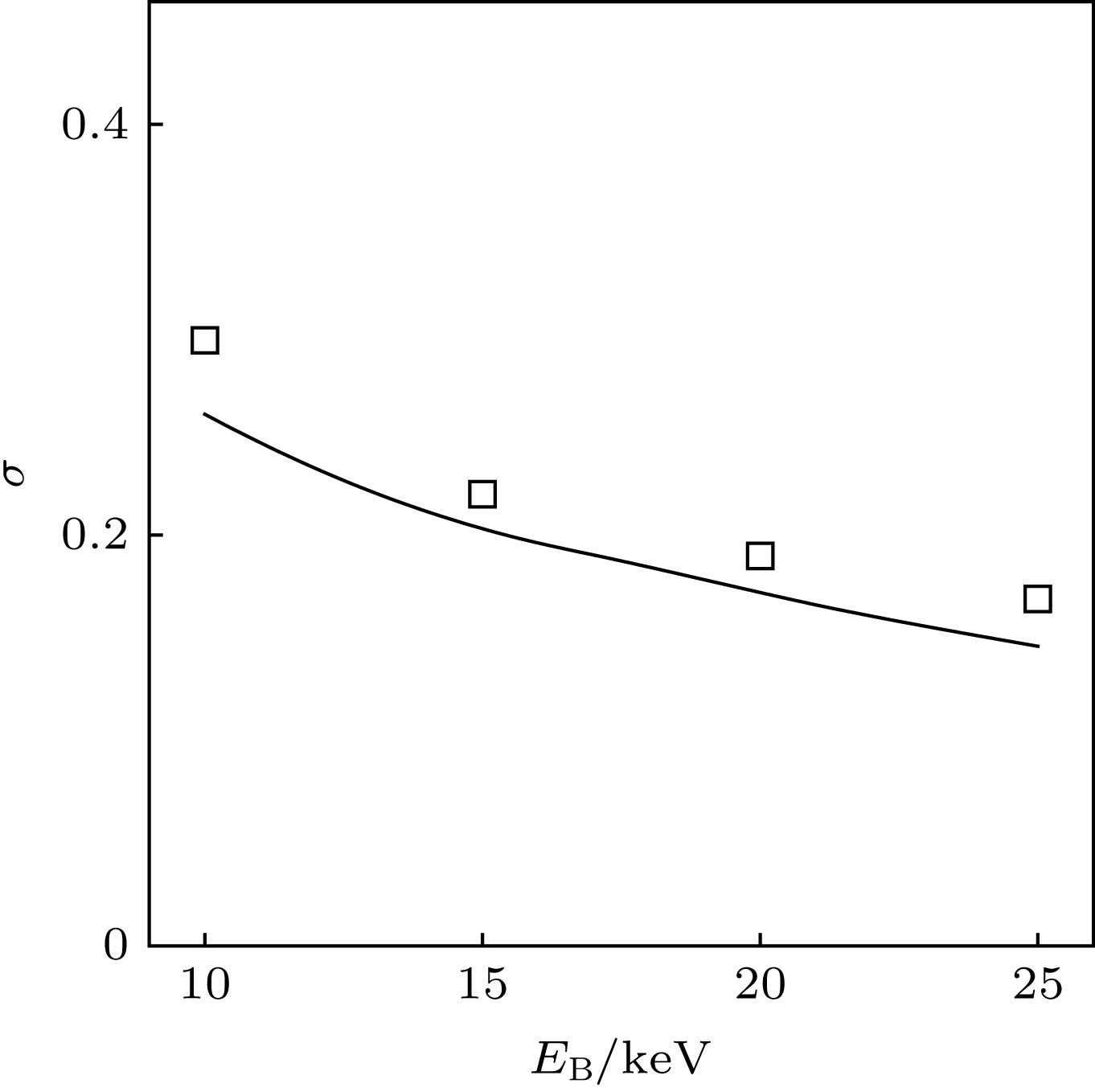
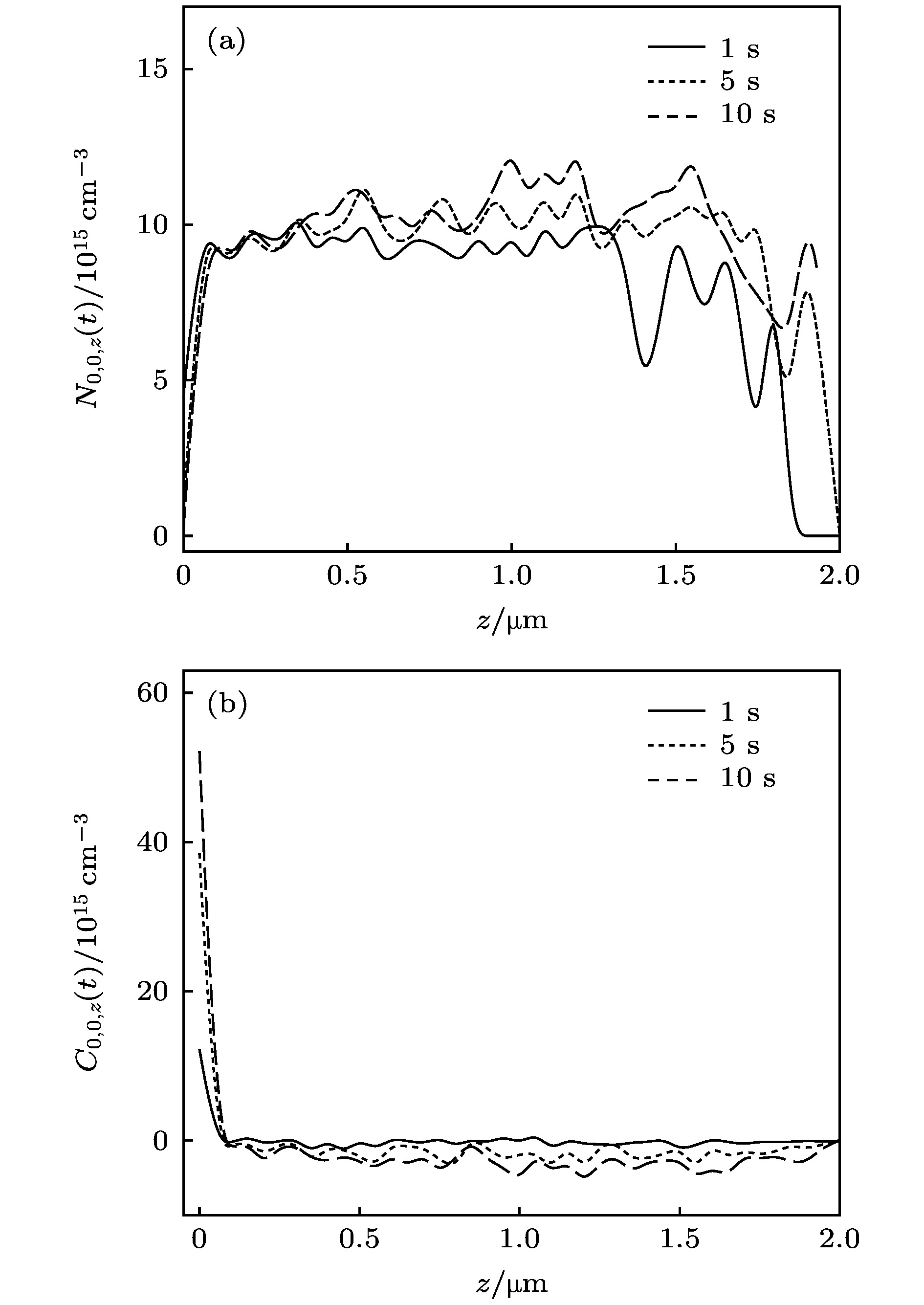
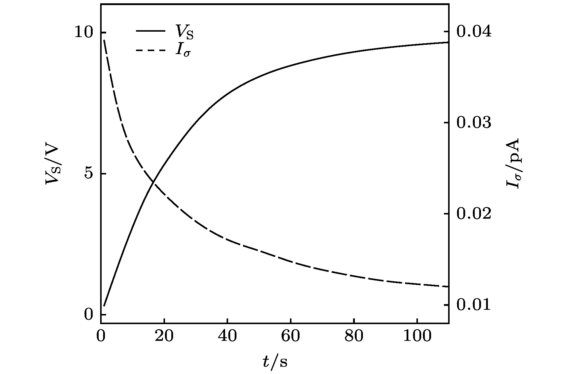
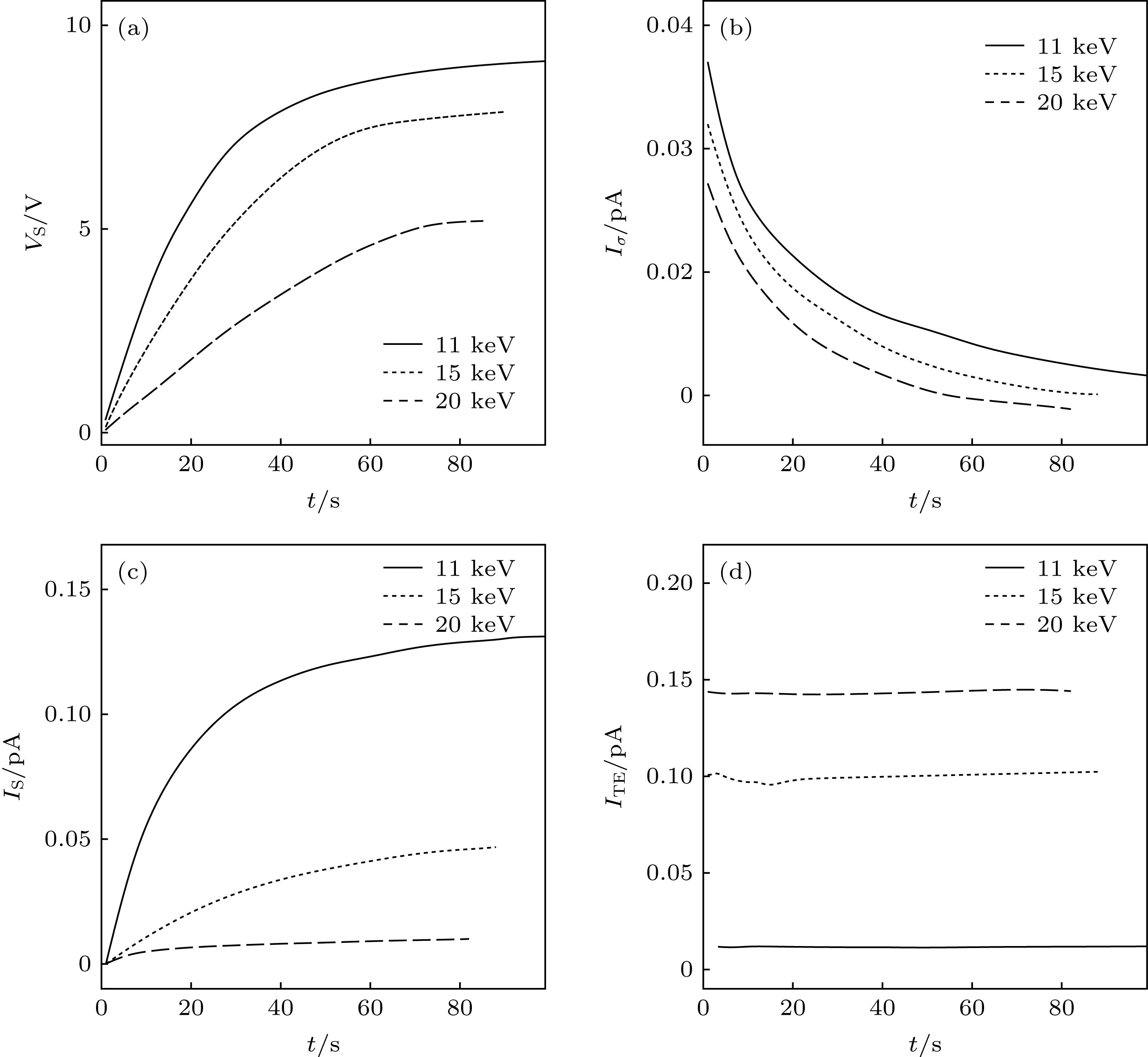
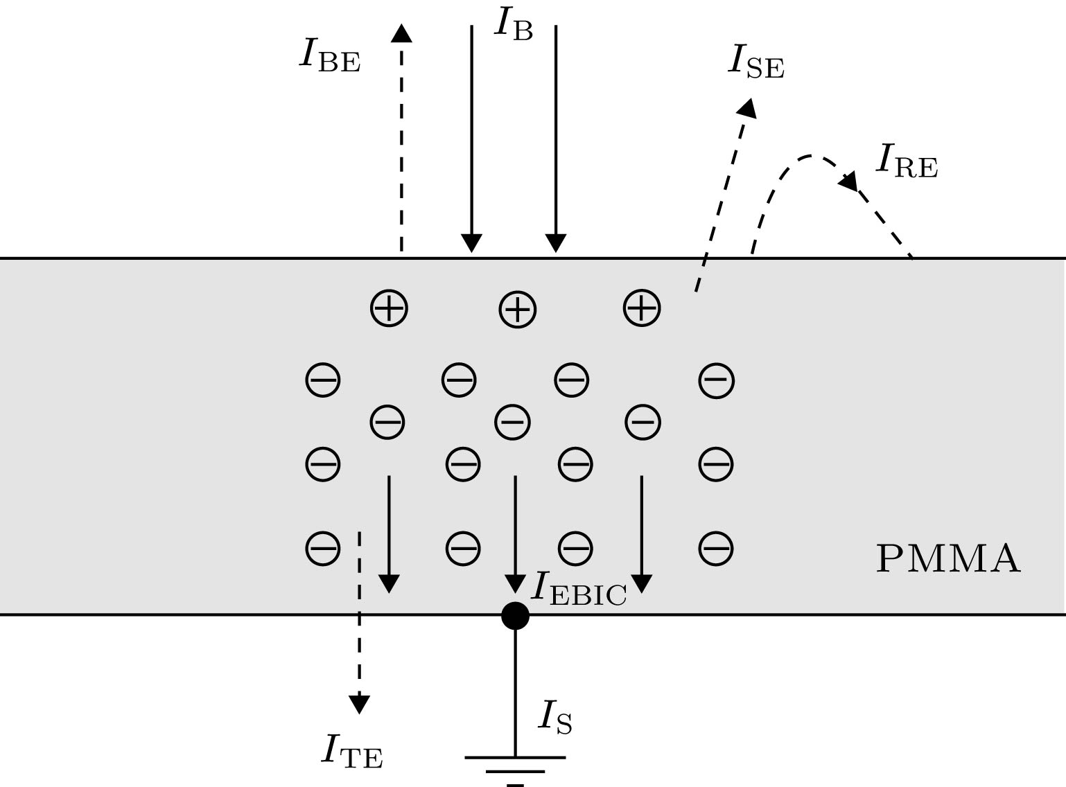
The serious charging effect of polymer film with a thickness of the order of microns under the radiation of high-energy transmission electron beam, on the reliability of the micro-nano electronic device in electron microscopy detection is investigated. The charging effect of the polymer film is numerically calculated in this paper. The scattering process is simulated by the Monte Carlo method. The elastic scattering is calculated with the Rutherford scattering model. The inelastic scattering is simulated with the fast secondary electron (SE) model and the Penn model. The transport, the capture, and the recombination process of the charges are treated with the finite difference method. The fourth-order Runge-Kutta method is used to solve the trajectory of the emitted SEs. The dynamic distributions of the net charge, the built-in electric field, the surface emission current, and the transmission current are investigated, and the influence of the film thickness and the beam energy on the charging characteristics are analyzed. The results show that due to the emission of electrons near the sample surface, the distribution of the net charge in the sample is first positive and then negative along the incident direction. In addition, under the irradiation,higher charge quantity is deposited in the sample, and the net charge density increases gradually. However, with long-time irradiation, the deposited electrons transport to the surface under the action of built-in electric field which reduces the surface net charge density. Therefore the net charge density tends to a stable value. The space potential is positive in the surface and negative inside the sample. Therefore some emitted SEs return to the surface, resulting in the electron beam-induced current. With the irradiation, the positive surface potential increases and tends to a stable value. Hence the actual surface emission current decreases to a stable value and the sample current increases to a stable value. The sample current remains unchanged due to the weak charging strength. Increasing the film thickness leads the transient time to increase, which contributes to the decline of the surface potential and the increase of the actual emission currentand sample current. The increase of the beam energy causes the transmission current to increase and the sample current to decrease. In addition, it reduces the positive surface potential and the actual surface emission current accordingly. The results conduce to the decrease of the charging effect of the polymer film under the radiation of high-energy electron beam in the electron microscopy.
-
Keywords:
- charging effect /
- numerical simulation /
- transmission current /
- transport
[1] Zhang M, Wang X X, Cao W Q, Yuan J, Cao M S 2019 Adv. Optical Mater. 6 1900689
[2] Cao M S, Wang X X, Zhang M, Shu J C, Cao W Q, Yang H J, Fang X Y, Yuan J 2019 Adv. Funct. Mater. 29 1807398
 Google Scholar
[3] Reimer L 1993 Image Formation in Low Voltage Scanning Electron Microscopy (Bellingham: SPIE Optical Engineering Press) p71
[4] Fakhfakh S, Jbara O, Rondot S, Hadjadj A, Fakhfakh Z 2012 J. Non-Cryst. Solids 358 1157
 Google Scholar
[5] Jbara O, Fakhfakh S, Belhaj M, Rondot S, Hadjadj A, Patat J M 2008 J. Phys. D 41 245504
 Google Scholar
[6] Belhaj M, Paulmier T, Hanna R, Arnaout M, Balcon N, Payan D, Puech J 2014 Nucl. Instrum. Methods Phys. Rec., Sect. B 320 46
 Google Scholar
[7] Paulmier T, Dirassen B, Payan D, Eesbeek M V 2009 IEEE Trans. Dielectr. Electr. Insul. 16 682
 Google Scholar
[8] 黄建国, 韩建伟 2010 59 2907
 Google Scholar
Huang J G, Han J W 2010 Acta Phys. Sin. 59 2907
 Google Scholar
[9] Ben Ammar L, Fakhfakh S, Jbara O, Rondot S 2017 J. Microsc. 265 322
 Google Scholar
[10] Cazaux J 2010 J. Electron Spectrosc. Relat. Phenom. 176 58
 Google Scholar
[11] Cornet N, Goeuriot D, Guerret-Piécourt C, Juvé D, Tréheux D, Touzin M, Fitting H J 2008 J. Appl. Phys. 103 064110
 Google Scholar
[12] Rau E I, Fakhfakh S, Andrianov M V, Evstafeva E N, Jbara O, Rondot S, Mouze Z 2008 Nucl. Instrum. Methods Phys. Res. Sect. B 266 719
 Google Scholar
[13] Cazaux J 2012 J. Electron Microsc. 61 261
 Google Scholar
[14] Rau E I, Tatarintsev A A 2012 J. Surf. Invest. 6 911
 Google Scholar
[15] Feng G B, Wang F, Hu T C, Cao M 2015 Chinese Phys. B 24 117901
 Google Scholar
[16] Pan S M, Min D M, Wang X P, Hou X B, Wang L, Li S T 2019 IEEE Trans. Nucl. Sci. 66 549
 Google Scholar
[17] Li W Q, Zhang H B 2010 Appl. Surf. Sci. 256 3482
 Google Scholar
[18] Li W Q, Mu K, Xia R H 2011 Micron 42 443
 Google Scholar
[19] 李维勤, 刘丁, 张海波 2014 63 227303
 Google Scholar
Li W Q, Liu D, Zhang H B 2014 Acta Phys. Sin. 63 227303
 Google Scholar
[20] 李维勤, 郝杰, 张海波 2015 64 086801
 Google Scholar
Li W Q, Hao J, Zhang H B 2015 Acta Phys. Sin. 64 086801
 Google Scholar
[21] Saloum S, Akel M, Alkhaled B 2009 J. Phys. D 42 085201
 Google Scholar
[22] Barman P, Singh M S, Maibam J, Brojen R K, Sharma B I 2010 Ind. J. Phys. 84 711
 Google Scholar
[23] 翁明, 胡天存, 曹猛, 徐伟军 2015 64 157901
 Google Scholar
Weng M, Hu T C, Cao M, Xu W J 2015 Acta Phys. Sin. 64 157901
 Google Scholar
[24] 封国宝, 曹猛, 崔万照, 李军, 刘纯亮, 王芳 2017 66 067901
 Google Scholar
Feng G B, Cao M, Cui W Z, Li J, Liu C L, Wang F 2017 Acta Phys. Sin. 66 067901
 Google Scholar
[25] Joy D C 1995 Monte Carlo Modeling for Electron Microscopy and Microanalysis (New York: Oxford University Press) p27
[26] You D S, Li H M, Ding Z J 2018 J. Electron Spectrosc. Relat. Phenom. 222 156
 Google Scholar
[27] Da B, Mao S F, Zhang G H, Ding Z J 2012 J. Appl. Phys. 112 034310
 Google Scholar
[28] Touzin M, Goeuriot D, Guerret-Piécourt C, Juvé D, Tréheux D, Fitting H J 2006 J. Appl. Phys. 99 114110
 Google Scholar
[29] Cao M S, Shu J C, Wang X X, Wang X, Zhang M, Yang H J, Fang X, Yuan J 2019 Annalen Der Physik 531 1800390
 Google Scholar
[30] Fang X Y, Yu X X, Zheng H M, Jin H B, Wang L, Cao M S 2015 Phys. Lett. A 379 2245
 Google Scholar
[31] Li S L, Yu X X, Li Y L, Jia Y H, Fang X Y, Cao M S 2019 Eur. Phys. J. B 92 155
 Google Scholar
[32] Song Z G, Ong C K, Gong H 1997 Appl. Surf. Sci. 119 169
 Google Scholar
[33] Sessler G M 1992 IEEE T. Electr. Insul. 27 961
 Google Scholar
[34] Sessler G M, Figueiredo M T, Ferreria G F L 2004 IEEE T. Dielect. El. Inl. 11 192
[35] Li Y J, Li S L, Gong P, Li Y L, Fang X Y, Jia Y H, Cao M S 2018 Physica E 104 247
 Google Scholar
[36] Rau E I 2008 Appl. Surf. Sci. 254 2110
 Google Scholar
-
表 1 参数默认取值
Table 1. Default values of parameters.
参数 取值 单位 电子束能量EB 10 keV 束流 0.16 pA 样品厚度H 2 μm 复合率 10–14 cm–3·s–1 电子迁移率μ 10–10 cm2·V–1·s–1 陷阱体密度Ntrap 1017 cm–3 -
[1] Zhang M, Wang X X, Cao W Q, Yuan J, Cao M S 2019 Adv. Optical Mater. 6 1900689
[2] Cao M S, Wang X X, Zhang M, Shu J C, Cao W Q, Yang H J, Fang X Y, Yuan J 2019 Adv. Funct. Mater. 29 1807398
 Google Scholar
[3] Reimer L 1993 Image Formation in Low Voltage Scanning Electron Microscopy (Bellingham: SPIE Optical Engineering Press) p71
[4] Fakhfakh S, Jbara O, Rondot S, Hadjadj A, Fakhfakh Z 2012 J. Non-Cryst. Solids 358 1157
 Google Scholar
[5] Jbara O, Fakhfakh S, Belhaj M, Rondot S, Hadjadj A, Patat J M 2008 J. Phys. D 41 245504
 Google Scholar
[6] Belhaj M, Paulmier T, Hanna R, Arnaout M, Balcon N, Payan D, Puech J 2014 Nucl. Instrum. Methods Phys. Rec., Sect. B 320 46
 Google Scholar
[7] Paulmier T, Dirassen B, Payan D, Eesbeek M V 2009 IEEE Trans. Dielectr. Electr. Insul. 16 682
 Google Scholar
[8] 黄建国, 韩建伟 2010 59 2907
 Google Scholar
Huang J G, Han J W 2010 Acta Phys. Sin. 59 2907
 Google Scholar
[9] Ben Ammar L, Fakhfakh S, Jbara O, Rondot S 2017 J. Microsc. 265 322
 Google Scholar
[10] Cazaux J 2010 J. Electron Spectrosc. Relat. Phenom. 176 58
 Google Scholar
[11] Cornet N, Goeuriot D, Guerret-Piécourt C, Juvé D, Tréheux D, Touzin M, Fitting H J 2008 J. Appl. Phys. 103 064110
 Google Scholar
[12] Rau E I, Fakhfakh S, Andrianov M V, Evstafeva E N, Jbara O, Rondot S, Mouze Z 2008 Nucl. Instrum. Methods Phys. Res. Sect. B 266 719
 Google Scholar
[13] Cazaux J 2012 J. Electron Microsc. 61 261
 Google Scholar
[14] Rau E I, Tatarintsev A A 2012 J. Surf. Invest. 6 911
 Google Scholar
[15] Feng G B, Wang F, Hu T C, Cao M 2015 Chinese Phys. B 24 117901
 Google Scholar
[16] Pan S M, Min D M, Wang X P, Hou X B, Wang L, Li S T 2019 IEEE Trans. Nucl. Sci. 66 549
 Google Scholar
[17] Li W Q, Zhang H B 2010 Appl. Surf. Sci. 256 3482
 Google Scholar
[18] Li W Q, Mu K, Xia R H 2011 Micron 42 443
 Google Scholar
[19] 李维勤, 刘丁, 张海波 2014 63 227303
 Google Scholar
Li W Q, Liu D, Zhang H B 2014 Acta Phys. Sin. 63 227303
 Google Scholar
[20] 李维勤, 郝杰, 张海波 2015 64 086801
 Google Scholar
Li W Q, Hao J, Zhang H B 2015 Acta Phys. Sin. 64 086801
 Google Scholar
[21] Saloum S, Akel M, Alkhaled B 2009 J. Phys. D 42 085201
 Google Scholar
[22] Barman P, Singh M S, Maibam J, Brojen R K, Sharma B I 2010 Ind. J. Phys. 84 711
 Google Scholar
[23] 翁明, 胡天存, 曹猛, 徐伟军 2015 64 157901
 Google Scholar
Weng M, Hu T C, Cao M, Xu W J 2015 Acta Phys. Sin. 64 157901
 Google Scholar
[24] 封国宝, 曹猛, 崔万照, 李军, 刘纯亮, 王芳 2017 66 067901
 Google Scholar
Feng G B, Cao M, Cui W Z, Li J, Liu C L, Wang F 2017 Acta Phys. Sin. 66 067901
 Google Scholar
[25] Joy D C 1995 Monte Carlo Modeling for Electron Microscopy and Microanalysis (New York: Oxford University Press) p27
[26] You D S, Li H M, Ding Z J 2018 J. Electron Spectrosc. Relat. Phenom. 222 156
 Google Scholar
[27] Da B, Mao S F, Zhang G H, Ding Z J 2012 J. Appl. Phys. 112 034310
 Google Scholar
[28] Touzin M, Goeuriot D, Guerret-Piécourt C, Juvé D, Tréheux D, Fitting H J 2006 J. Appl. Phys. 99 114110
 Google Scholar
[29] Cao M S, Shu J C, Wang X X, Wang X, Zhang M, Yang H J, Fang X, Yuan J 2019 Annalen Der Physik 531 1800390
 Google Scholar
[30] Fang X Y, Yu X X, Zheng H M, Jin H B, Wang L, Cao M S 2015 Phys. Lett. A 379 2245
 Google Scholar
[31] Li S L, Yu X X, Li Y L, Jia Y H, Fang X Y, Cao M S 2019 Eur. Phys. J. B 92 155
 Google Scholar
[32] Song Z G, Ong C K, Gong H 1997 Appl. Surf. Sci. 119 169
 Google Scholar
[33] Sessler G M 1992 IEEE T. Electr. Insul. 27 961
 Google Scholar
[34] Sessler G M, Figueiredo M T, Ferreria G F L 2004 IEEE T. Dielect. El. Inl. 11 192
[35] Li Y J, Li S L, Gong P, Li Y L, Fang X Y, Jia Y H, Cao M S 2018 Physica E 104 247
 Google Scholar
[36] Rau E I 2008 Appl. Surf. Sci. 254 2110
 Google Scholar
Catalog
Metrics
- Abstract views: 8671
- PDF Downloads: 64
- Cited By: 0


 DownLoad:
