-
The unidirectional propagation of the pseudospin-locked optical waves can be achieved by using the helical edge states in two-dimensional topological spin photonic crystals. Although there have been lots of researches on topological spin photonic crystal, the unidirectional propagation regulation of helical edge states has been rarely studied up to now. Herein, by tuning the diameter D of the dielectric rod and the distance R between the center of the unit cell and the center of the rod in two-dimensional topological spin photonic crystal with C6v symmetry, the effects of geometric parameters on the bandgap structure, topological properties and unidirectional propagation of helical edge states in topological spin photonics crystals are studied in detail. The results show that the parameter R has significant effects on the bandgap structure and topological properties of topological spin photonic crystal, and the diameter D of rod only affects the bandgap positions. The structures of helical edge states and their unidirectional propagations are closely related to the topological properties of the bandgaps and the frequency structures of photonic crystals on both sides of boundary. Without changing the topological properties of bandgaps, only changing the structures of the photonics crystals on either side of the boundary can also regulate the structures of the helical edge states and their unidirectional propagation. Thus, by adjusting the geometric parameters R and D of the topological spin photonic crystals, the helical edge states and their unidirectional propagations can be controlled. This study provides useful references for the selection and application of helical edge states in topological spin photonic crytals.
-
Keywords:
- topological /
- spin /
- photonic crystal /
- edge state
[1] Lu L, Joannopoulos J D, Soljačić M 2014 Nat. Photonics 8 821
 Google Scholar
[2] Hasan M Z, Kane C L 2010 Rev. Mod. Phys. 82 3045
 Google Scholar
[3] 吕新宇, 李志强 2019 68 220303
 Google Scholar
Lv X Y, Li Z Q 2019 Acta Phys. Sin. 68 220303
 Google Scholar
[4] Wu Y, Li C, Hu X Y, Ao Y T, Zhao Y F, Gong Q H 2017 Adv. Opt. Mater. 5 1700357
[5] Ozawa T, Price H M, Amo A, Goldman N, Hafezi M, Lu L, Rechtsman M C, Schuster D, Simon J, Zilberberg O, Carusotto L 2019 Rev. Mod. Phys. 91 015006
 Google Scholar
[6] 王彦兰, 李妍 2020 69 094206
 Google Scholar
Wang Y L, Li Y 2020 Acta Phys. Sin. 69 094206
 Google Scholar
[7] Haldane F M, Raghu S 2008 Phys. Rev. Lett. 100 013904
 Google Scholar
[8] Wang Z, Chong Y D, Joannopoulos J D, Soljačić M 2008 Phys. Rev. Lett. 100 013905
 Google Scholar
[9] Wang Z, Chong Y D, Joannopoulos J D, Soljačić M 2009 Nature 461 772
 Google Scholar
[10] Yin P, Wu R X, Lin Z, Yang Y, Chan C T 2011 Phys. Rev. Lett. 106 093903
 Google Scholar
[11] Skirlo S A, Lu L, Soljacic M 2014 Phys. Rev. Lett. 113 113904
 Google Scholar
[12] Yang B, Wu T, Zhang X D 2017 Appl. Phys. Lett. 110 021109
 Google Scholar
[13] Chan H C, Guo G Y 2018 Phys. Rev. B 97 45422
 Google Scholar
[14] Yang B, Zhang H F, Shi Q, Wu T, Ma Y, Lv Z T, Xiao X, Dong R X, Yan X L, Zhang X D 2020 Opt. Express 28 31487
 Google Scholar
[15] 陈剑锋, 梁文耀, 李志远 2021 光学学报 41 0823015
 Google Scholar
Chen J F, Liang W Y, Li Z Y 2021 Acta Opt. Sin. 41 0823015
 Google Scholar
[16] Hafezi M, Mittal S, Fan J, Migdall A, Taylor J M 2013 Nat. Photonics 7 1001
 Google Scholar
[17] Rechtsman M C, Zeuner J M, Plotnik Y, Lumer Y, Podolsky D, Dreisow F, Nolte S, Segev M, Szameit A 2013 Nature 496 196
 Google Scholar
[18] Mukherjee S, Spracklen A, Valiente M, Andersson E, Öhberg P, Goldman N, Thomson R R 2017 Nat. Commun. 8 13918
 Google Scholar
[19] Maczewsky L J, Zeuner J M, Nolte S, Szameit A 2017 Nat. Commun. 8 13756
 Google Scholar
[20] Chen W J, Jiang S J, Chen X D, Zhu B, Zhou L, Dong J W 2014 Nat. Commun. 5 5782
 Google Scholar
[21] Wu L H, Hu X 2015 Phys. Rev. Lett. 114 223901
 Google Scholar
[22] 方云团, 王张鑫, 范尔盼, 李小雪, 王洪金 2020 69 184101
 Google Scholar
Fang Y T, Wang Z X, Fan E P, Li X X, Wang H J 2020 Acta Phys. Sin. 69 184101
 Google Scholar
[23] Jin M C, Gao Y F, Ma Q L, Zhang W, Song H, Sun J P 2021 Phys. Rev. Mater. 5 024204
 Google Scholar
[24] Li Z, Chan H C, Xiang Y 2020 Phys. Rev. B 102 245149
 Google Scholar
[25] Xu L, Wang H X, Xu Y D, Chen H Y, Jiang J H 2016 Opt. Express 24 18059
 Google Scholar
[26] Fang Y T, Wang Z X. 2021 Opt. Commun. 479 126451
 Google Scholar
[27] Yang Y T, Xu Y F, Xu T, Wang H X, Jiang J H, Hu X, Hang Z H 2018 Phys. Rev. Lett. 120 217401
 Google Scholar
[28] Yang Y T, Qian X Y, Shi L W, Shen X P, Wang Y F, Hang Z H 2022 Opt. Express 30 5731
 Google Scholar
[29] Chen X D, Deng W M, Shi F L, Zhao F L, Chen M, Dong J W 2019 Phys. Rev. Lett. 122 233902
 Google Scholar
[30] Tang G J, He X T, Shi F L, Liu J W, Chen X D, Dong J W 2022 Laser Photonics Rev. 16 2100300
 Google Scholar
[31] Xu X F, Huang J Y, Zhang H, Guo X Y, Mu S S, Liu Y Q, Zhai N 2021 Opt. Commun. 498 127262
 Google Scholar
[32] 刘慧, 王好南, 谢博阳, 程化, 田建国, 陈树琪 2021 中国光学 14 20
 Google Scholar
Liu H, Wang H N, Xie B Y, Cheng H, Tian J G, Chen S Q 2021 Chin. Opt. 14 20
 Google Scholar
[33] Joannopoulos J D, Johnson S G, Winn J N, Meade R D 2008 Photonic Crystals: Molding The Flow of Light (2nd Ed) (New Jersey: Princeton University Press) pp80–93
[34] Yang B, Zhang H F, Wu T, Dong R X, Yan X L, Zhang X D 2019 Phys. Rev. B 99 045307
 Google Scholar
[35] Jiang Z, Gao Y F, He L, Sun J P, Song H, Wang Q 2019 Phys. Chem. Chem. Phys. 21 11367
 Google Scholar
-
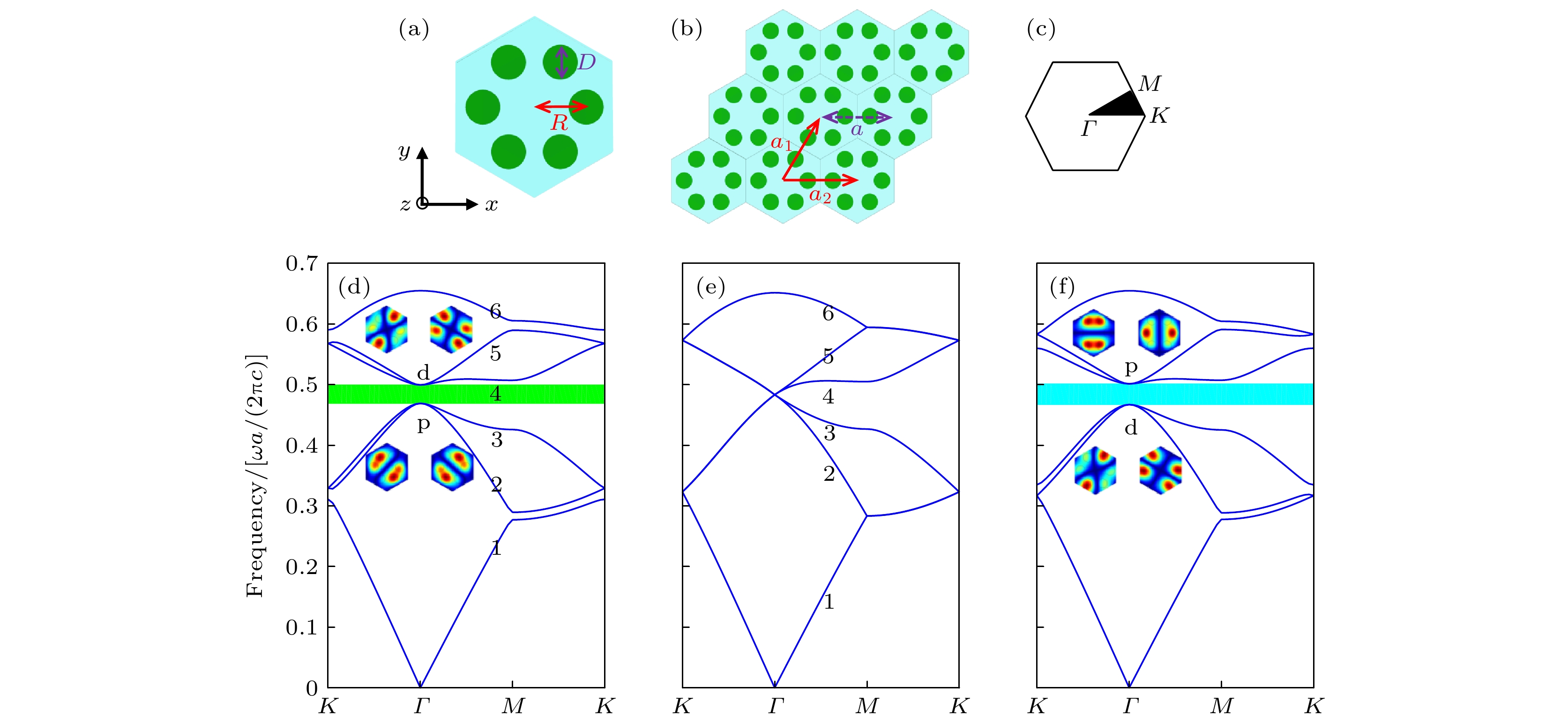
图 1 (a)二维三角晶格光子晶体原胞; (b)光子晶体周期结构; (c)三角晶格光子晶体的第一布里渊区; (d)—(f)当D = 2a/9时, R分别取a/3 – 0.02a, a/3和a/3 + 0.02a时, 光子晶体的频带结构; (d)和(f)中插图为相应的Г点处p轨道和d轨道的本征模场|Ez|
Figure 1. (a) Primitive cell of two-dimensional triangular lattice; (b) periodic structure of photonic crystal; (c) the first Brillouin zone of the periodic structure; (d)–(f) frequency band structures as D = 2a/9 and R takes values of a/3–0.02a, a/3 and a/3 + 0.02a, respectively; inserts in (d) and (f) show the distributions of eigenfields |Ez| of p and d orbits at point Г
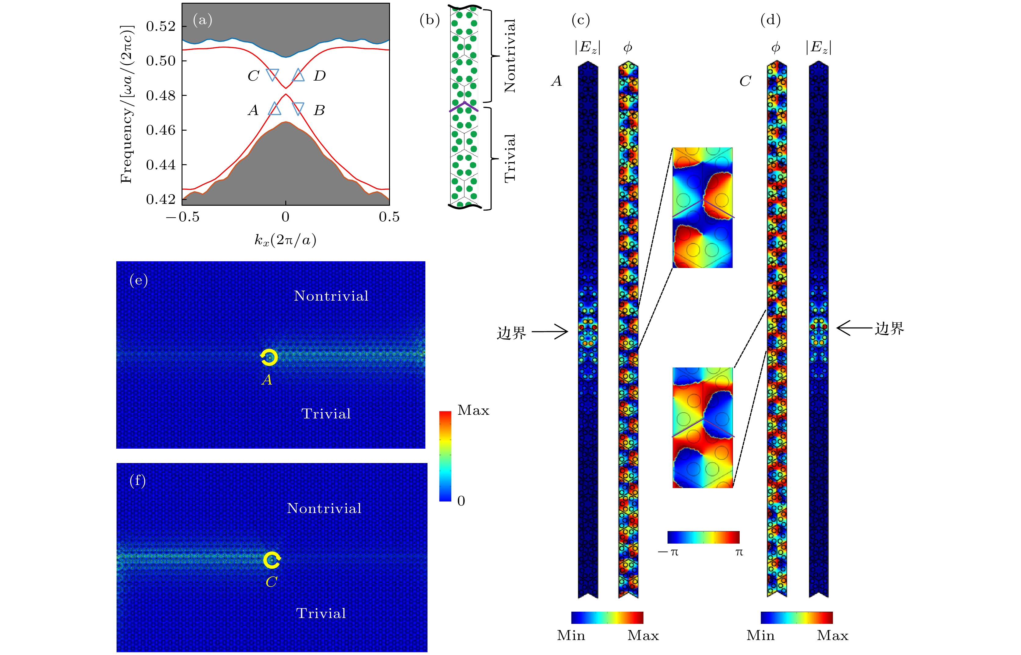
图 2 (a)赝自旋拓扑性质不同的光子晶体结构界面处的投影边界态, 阴影部分为体态, 红色曲线为螺旋边界态; (b)用于计算投影边界态的超原胞结构示意图; (c)和(d)分别与(a)图中A点和C点边界态对应的本征模场|Ez|及相位分布ϕ = arg(Ez); (e)和(f)分别与(a)图中A点和C点边界态对应的由赝自旋光源激发的光传播模拟图, 其中环形箭头表示赝自旋光源所在的位置, 箭头旋转方向表示光源的自旋方向
Figure 2. (a) Projected diagram of edge state at boundary of two photonic crystals with different pseudospin topological properties, shaded areas are bulk states, and red curves are helical edge states; (b) supercell for calculation of projected diagram; (c) and (d) the eigenfield |Ez| and phase distribution ϕ = arg(Ez) of edge states A and C in (a), respectively; (e) and (f) propagation simulation of edge states A and C excited by pseudospin sources, the yellow circular arrows denote locations of sources, and rotation directions of arrows indicate spin directions of sources.
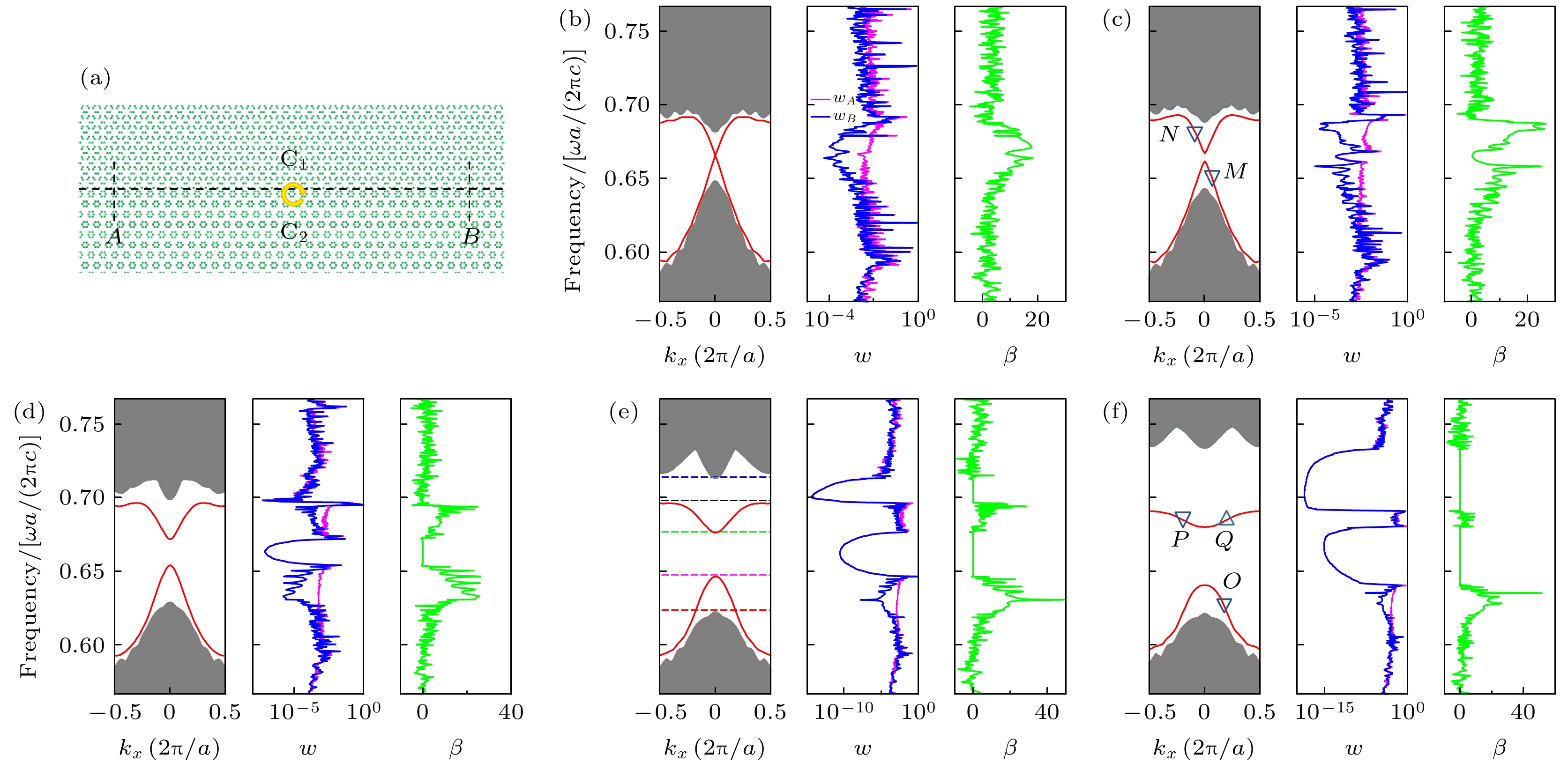
图 4 (a)模型结构示意图; (b)—(f)当D=0.13a时, 分别取r值为0.01a, 0.02a, 0.04a, 0.06a和0.08a时系统的投影边界态以及赝自旋光波在边界处的单向传输效果图, 左侧图: 投影边界态, 中间图: 光波能量wA和wB, 右侧图: 单向隔离率β; (e)中蓝、黑、绿、洋红、红色虚线(由上至下)分别对应上体态带底、上边界态带顶、上边界态带底、下边界态带顶和下体态带顶处的频率位置; (c)中M和N两点分别对应频率0.648的下边界态和频率0.684的上边界态; (f)中O点对应频率0.622的下边界态、P和Q点对应频率0.685的两上边界态
Figure 4. (a) Schematic diagram of calculation model; (b)–(f) projected diagram of edge states and unidirectional propagation of pseudospin wave at boundaries as D = 0.13a and r takes values of 0.01a, 0.02a, 0.04a, 0.06a and 0.08a, respectively. Left panel: projected diagram, central panel: optical energy wA and wB, right panel: unidirectional isolation rate β. In (e), the blue , black, green, magenta and red dashed lines (top to bottom) represent frequency positions of bottom of upper body state, top of upper edge state, bottom of upper edge state, top of lower edge state and top of lower body state, respectively. In (c), points M and N mark the lower edge state with frequency 0.648 and upper edge state with frequency 0.684, respectively. In (f), point O marks the lower edge state with frequency 0.622, points P and Q mark the upper edge states with frequency 0.685.
图 7 (a)—(c)当R1 = 0.21a, R2 = 0.41a时, D1 = D2 = D, 并分别取D为0.1a, 0.13a, 0.16a时系统的投影边界态图及赝自旋光波在边界处的单向传输效果图, 左侧图: 投影边界态, 中间图: 光波能量wA和wB, 右侧图: 单向隔离率β; (d)随着D增大, 螺旋边界态的演化, 图中曲线类型及颜色标记同图5; (e)和(f)赝自旋光源激发的(b)图中E和F点处边界态在界面处的传播
Figure 7. (a)–(c) Projected diagram of edge states and unidirectional propagation of pseudospin wave at boundaries as R1 = 0.21a, R2 = 0.41a, D1 = D2 = D and D takes values of 0.1a, 0.13a and 0.16a, respectively. Left panel: projected diagram, central panel: optical energy wA and wB, right panel: unidirectional isolation rate β. (d) Variation of helical edge states as D increases, the curve types and color legends are the same as those in Fig.5. (e) and (f) Propagation simulation of the edge states of points E and F in (b), respectively, exited by pseudospin sources.
图 8 上行图边界处激发光源附近本征场Ez的相位分布(a)—(d)分别对应图4(c)中M, N点和图4(f)中O, P点边界态相位分布;(e)自由空间中赝自旋光源的电场相位分布. 下行各图对应上行各图中白色圆圈路径上的光场的相位变化, 激发光源位于白色圆圈中心
Figure 8. Upper panels: Phase distributions ϕ = arg(Ez) of the eigenfield around excited sources at boundaries, (a)–(d) corresponding to the edge states of points M and N in Fig.4(c), and points O and P in Fig.4(f), respectively; (e) pseudospin source in free space, lower panels: variation of the phase distributions along the white circle in each upper panel, the excited source locates at the center of each white circle.
图 9 (a)—(c) C1, C2和C3结构光子晶体的频带结构, (c)中插图为其第4个频带Г点处的本征模场|Ez|; (d)和(e) C12结构和C13结构的赝自旋螺旋边界态及其单向传输效果图. 左侧图: 投影边界态, 中间图: 光波能量wA和wB, 右侧图: 单向隔离率β. (f)—(i)分别对应C12结构中赝自旋光源激发的(d)图中S点和T点边界态以及C13结构中赝自旋光源激发的(e)图中U点和V点边界态在界面处的传播
Figure 9. (a)–(c) Band structures of the photonic crystals of C1, C2 and C3, respectively, insert in (c) shows the eigenfield |Ez| of Гof the 4th band; (d) and (e) projected diagram of edge states and unidirectional propagation of pseudospin wave at boundaries of C12 and C13 structures, respectively. Left panel: projected diagram, central panel: optical energy wA and wB, right panel: unidirectional isolation rate β. (f)–(i) Propagation simulation of the edge states of points S and T in (d) of C12 structure, and edge states of points U and V in (e) of C13 structure, respectively, exited by pseudospin sources.
-
[1] Lu L, Joannopoulos J D, Soljačić M 2014 Nat. Photonics 8 821
 Google Scholar
[2] Hasan M Z, Kane C L 2010 Rev. Mod. Phys. 82 3045
 Google Scholar
[3] 吕新宇, 李志强 2019 68 220303
 Google Scholar
Lv X Y, Li Z Q 2019 Acta Phys. Sin. 68 220303
 Google Scholar
[4] Wu Y, Li C, Hu X Y, Ao Y T, Zhao Y F, Gong Q H 2017 Adv. Opt. Mater. 5 1700357
[5] Ozawa T, Price H M, Amo A, Goldman N, Hafezi M, Lu L, Rechtsman M C, Schuster D, Simon J, Zilberberg O, Carusotto L 2019 Rev. Mod. Phys. 91 015006
 Google Scholar
[6] 王彦兰, 李妍 2020 69 094206
 Google Scholar
Wang Y L, Li Y 2020 Acta Phys. Sin. 69 094206
 Google Scholar
[7] Haldane F M, Raghu S 2008 Phys. Rev. Lett. 100 013904
 Google Scholar
[8] Wang Z, Chong Y D, Joannopoulos J D, Soljačić M 2008 Phys. Rev. Lett. 100 013905
 Google Scholar
[9] Wang Z, Chong Y D, Joannopoulos J D, Soljačić M 2009 Nature 461 772
 Google Scholar
[10] Yin P, Wu R X, Lin Z, Yang Y, Chan C T 2011 Phys. Rev. Lett. 106 093903
 Google Scholar
[11] Skirlo S A, Lu L, Soljacic M 2014 Phys. Rev. Lett. 113 113904
 Google Scholar
[12] Yang B, Wu T, Zhang X D 2017 Appl. Phys. Lett. 110 021109
 Google Scholar
[13] Chan H C, Guo G Y 2018 Phys. Rev. B 97 45422
 Google Scholar
[14] Yang B, Zhang H F, Shi Q, Wu T, Ma Y, Lv Z T, Xiao X, Dong R X, Yan X L, Zhang X D 2020 Opt. Express 28 31487
 Google Scholar
[15] 陈剑锋, 梁文耀, 李志远 2021 光学学报 41 0823015
 Google Scholar
Chen J F, Liang W Y, Li Z Y 2021 Acta Opt. Sin. 41 0823015
 Google Scholar
[16] Hafezi M, Mittal S, Fan J, Migdall A, Taylor J M 2013 Nat. Photonics 7 1001
 Google Scholar
[17] Rechtsman M C, Zeuner J M, Plotnik Y, Lumer Y, Podolsky D, Dreisow F, Nolte S, Segev M, Szameit A 2013 Nature 496 196
 Google Scholar
[18] Mukherjee S, Spracklen A, Valiente M, Andersson E, Öhberg P, Goldman N, Thomson R R 2017 Nat. Commun. 8 13918
 Google Scholar
[19] Maczewsky L J, Zeuner J M, Nolte S, Szameit A 2017 Nat. Commun. 8 13756
 Google Scholar
[20] Chen W J, Jiang S J, Chen X D, Zhu B, Zhou L, Dong J W 2014 Nat. Commun. 5 5782
 Google Scholar
[21] Wu L H, Hu X 2015 Phys. Rev. Lett. 114 223901
 Google Scholar
[22] 方云团, 王张鑫, 范尔盼, 李小雪, 王洪金 2020 69 184101
 Google Scholar
Fang Y T, Wang Z X, Fan E P, Li X X, Wang H J 2020 Acta Phys. Sin. 69 184101
 Google Scholar
[23] Jin M C, Gao Y F, Ma Q L, Zhang W, Song H, Sun J P 2021 Phys. Rev. Mater. 5 024204
 Google Scholar
[24] Li Z, Chan H C, Xiang Y 2020 Phys. Rev. B 102 245149
 Google Scholar
[25] Xu L, Wang H X, Xu Y D, Chen H Y, Jiang J H 2016 Opt. Express 24 18059
 Google Scholar
[26] Fang Y T, Wang Z X. 2021 Opt. Commun. 479 126451
 Google Scholar
[27] Yang Y T, Xu Y F, Xu T, Wang H X, Jiang J H, Hu X, Hang Z H 2018 Phys. Rev. Lett. 120 217401
 Google Scholar
[28] Yang Y T, Qian X Y, Shi L W, Shen X P, Wang Y F, Hang Z H 2022 Opt. Express 30 5731
 Google Scholar
[29] Chen X D, Deng W M, Shi F L, Zhao F L, Chen M, Dong J W 2019 Phys. Rev. Lett. 122 233902
 Google Scholar
[30] Tang G J, He X T, Shi F L, Liu J W, Chen X D, Dong J W 2022 Laser Photonics Rev. 16 2100300
 Google Scholar
[31] Xu X F, Huang J Y, Zhang H, Guo X Y, Mu S S, Liu Y Q, Zhai N 2021 Opt. Commun. 498 127262
 Google Scholar
[32] 刘慧, 王好南, 谢博阳, 程化, 田建国, 陈树琪 2021 中国光学 14 20
 Google Scholar
Liu H, Wang H N, Xie B Y, Cheng H, Tian J G, Chen S Q 2021 Chin. Opt. 14 20
 Google Scholar
[33] Joannopoulos J D, Johnson S G, Winn J N, Meade R D 2008 Photonic Crystals: Molding The Flow of Light (2nd Ed) (New Jersey: Princeton University Press) pp80–93
[34] Yang B, Zhang H F, Wu T, Dong R X, Yan X L, Zhang X D 2019 Phys. Rev. B 99 045307
 Google Scholar
[35] Jiang Z, Gao Y F, He L, Sun J P, Song H, Wang Q 2019 Phys. Chem. Chem. Phys. 21 11367
 Google Scholar
Catalog
Metrics
- Abstract views: 9024
- PDF Downloads: 233
- Cited By: 0


 DownLoad:


