


-
The potential, unexpected occurrence of dielectric multipactor on the dielectric surfaces in high-power radio frequency and microwave components has become a severe constraint in the research and development of space-borne payloads of space vehicles such as satellites and space stations on the ground and their long-term reliable operations in the orbit. In this experimental research, the single-surface multipactor occurring on the dielectric surface of a penetration flange originally designed for a vacuum chamber used in environmental simulation tests of spacecraft is experimentally investigated and compared with the corresponding full-wave simulated results. Under the excitation of periodic pulsed sinusoidal signals, the unusual experimental phenomena of intermittent local jumps of nulling signals in the process of multipactor are repeatedly observed based on an agile nulling experimental system. Taking advantage of the full-wave, three-dimensional (3D) particle-in-cell simulation tool, CST Particle Studio, the entire evolution process of the dielectric multipactor, from its onset to its saturation, is simulated and carefully examined. Combining the results obtained by full-wave 3D particle simulations, some physical explanations and discussion on such phenomena are presented. It is found that under the configuration parameters of pulse signals adopted in this multipactor experiment, the transition of a single-surface dielectric multipactor from its onset to the saturation state can be finished within a single pulse. However, its transition from the saturation state to turning off can last between consecutive pulses in the absence of any high-power radio frequency signals. The obtained result is important for both the theoretical study and the engineering development of high-power dielectric components, providing a new understanding of the dielectric multipactor occurring under the excitation of pulsed high-power electric fields.
-
Keywords:
- penetration flange /
- dielectric multipactor /
- experimental study /
- particle-in-cell
[1] Woode A, Petit J 1990 ESA J. 14 467
 Google Scholar
[2] Rozario N, Lenzing H F, Reardon K F, Zarro M S, Baran C G 1994 IEEE Trans. Microwave Theory Tech. 42 558
Google Scholar
[3] Yu M 2007 IEEE Microwave Mag. 8 88
Google Scholar
[4] Kishek R A, Lau Y Y, Ang L K, Valfells A, Gilgenbach, R M 1998 Phys. Plasmas 5 2120
Google Scholar
[5] Kishek R A, Lau Y Y 1998 Phys. Rev. Lett. 80 193
Google Scholar
[6] Chang C, Liu G, Tang C, Chen C, Fang J 2011 Phys. Plasmas 18 055702
Google Scholar
[7] Hatch A J 1966 Nucl. Instrum. Methods 41 261
Google Scholar
[8] Power J G, Gai W, Gold S H, et al. 2004 Phys. Rev. Lett. 92 164801
Google Scholar
[9] Neuber A, Hemmert D, Krompholz H, et al. 1999 J. Appl. Phys. 86 1724
Google Scholar
[10] Chang C, Zhu M, Verboncoeur J, et al. 2014 Appl. Phys. Lett. 104 253504
Google Scholar
[11] Iqbal A, Wong P Y, Wen D Q, et al. 2020 Phys. Rev. E 102 043201
Google Scholar
[12] Neuber A, Butch M, Krompholz H, et al. 2000 IEEE Trans. Plasma Sci. 28 1593
Google Scholar
[13] Anderson R B, Getty W D, Brake M L, et al. 2001 Rev. Sci. Instrum. 72 3095
Google Scholar
[14] Ang L K, Lau Y Y, Kishek R A, Gilgenbach R M 1998 IEEE Trans. Plasma Sci. 26 290
Google Scholar
[15] Kim H C, Verboncoeur J P 2005 Phys. Plasmas 12 123504
Google Scholar
[16] Sazontov A, Semenov V, Buyanova M, et al. 2005 Phys. Plasmas 12 093501
Google Scholar
[17] Shen F Z, Wang X B, Cui W Z, Ran L X 2020 IEEE Trans. Plasma Sci. 48 433
Google Scholar
[18] Zhang Z Y, Sun Y Z, Cui W Z, et al. 2019 IEEE Trans. Electron Devices 66 4921
Google Scholar
[19] 董烨, 董志伟, 杨温渊, 周前红, 周海京 2013 62 197901
Google Scholar
Dong Y, Dong Z W, Yang W Y, Zhou Q H, Zhou H J 2013 Acta Phys. Sin. 62 197901
Google Scholar
[20] 张雪, 王勇, 范俊杰, 张瑞 2014 63 227901
Google Scholar
Zhang X, Wang Y, Fan J J, Zhang R 2014 Acta Phys. Sin. 63 227901
Google Scholar
[21] Langellotti S V, Jordan N M, Lau Y Y, et al. 2020 IEEE Trans. Plasma Sci. 48 1942
Google Scholar
[22] Hemmert D, Neuber A, Dickens J, et al. 2000 IEEE Trans. Plasma Sci. 28 472
Google Scholar
[23] Vaughan J R M 1988 IEEE Trans. Electron Devices 35 1172
Google Scholar
[24] Wang X B, Shen J H, Wang J Y, et al. 2017 IEEE Trans. Microwave Theory Tech. 65 2734
Google Scholar
-
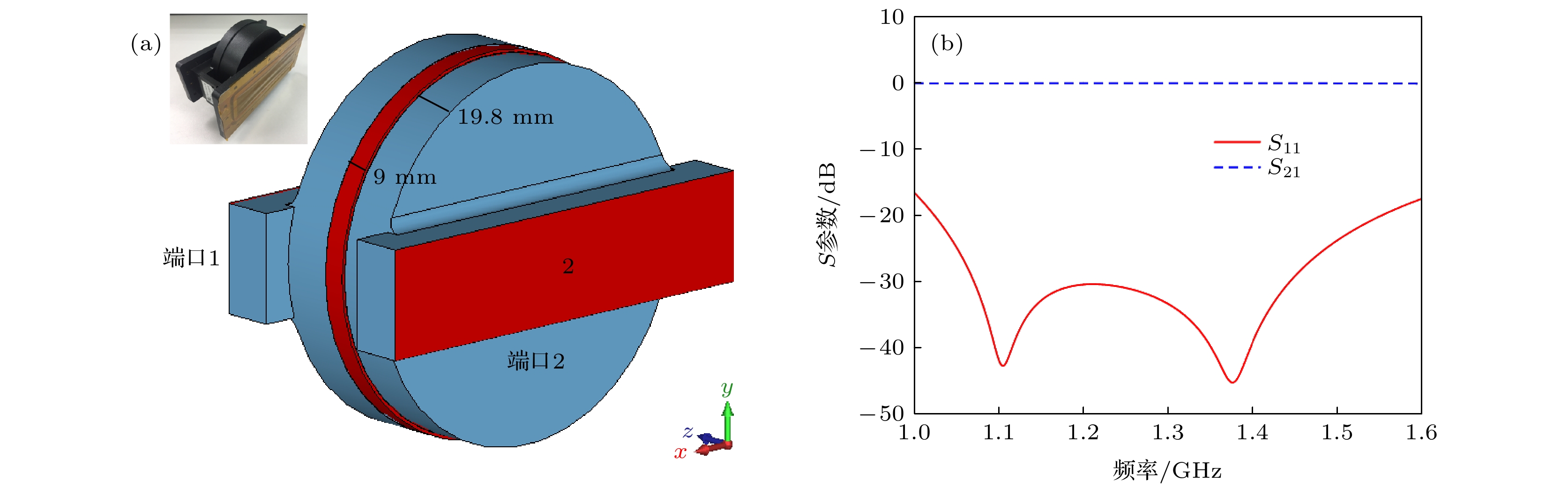
图 1 真空罐穿舱法兰的结构及其S参数 (a) 仿真模型及实物; (b) S参数
Figure 1. Structure of the penetration flange used in vacuum chambers and its S parameters: (a) Structure; (b) S parameters.
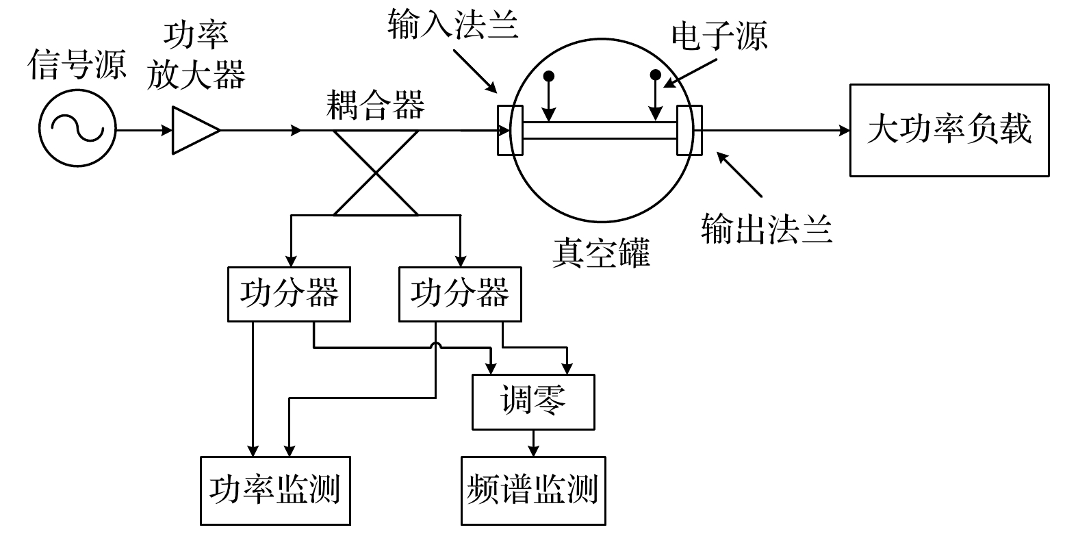
图 2 穿舱法兰微放电实验原理框图
Figure 2. Block diagram of the experimental setup.

图 3 微放电引起的调零信号跳变 (a)未发生微放电; (b)放电1; (c)放电2; (d)放电3
Figure 3. Jumps of nulling signals resulted by multipactors: (a) No multipacotr; (b) multipactor 1; (c) multipactor 2; (d) multipactor 3

图 4 微放电实验前后介质表面对比
Figure 4. Dielectric surfaces before and after a dielectric multipactor.
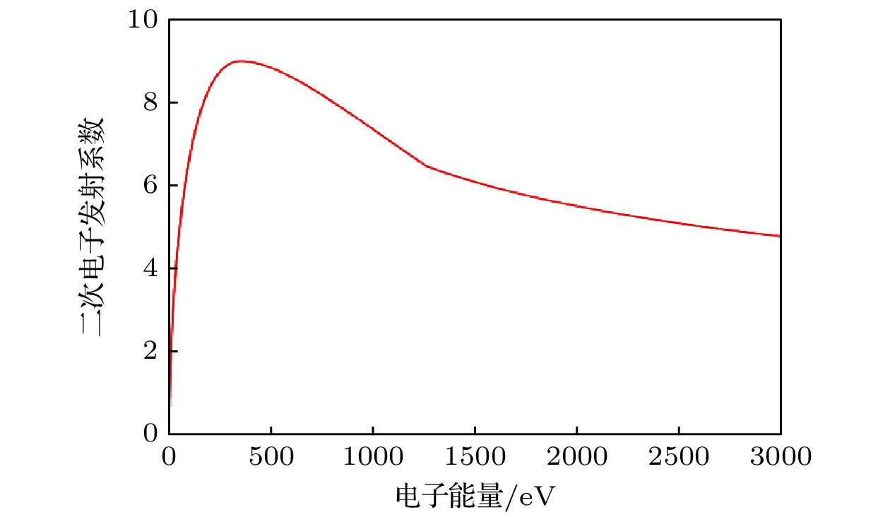
图 5 介质Al2O3的二次电子发射系数
Figure 5. Secondary emission yield of dielectric Al2O3.
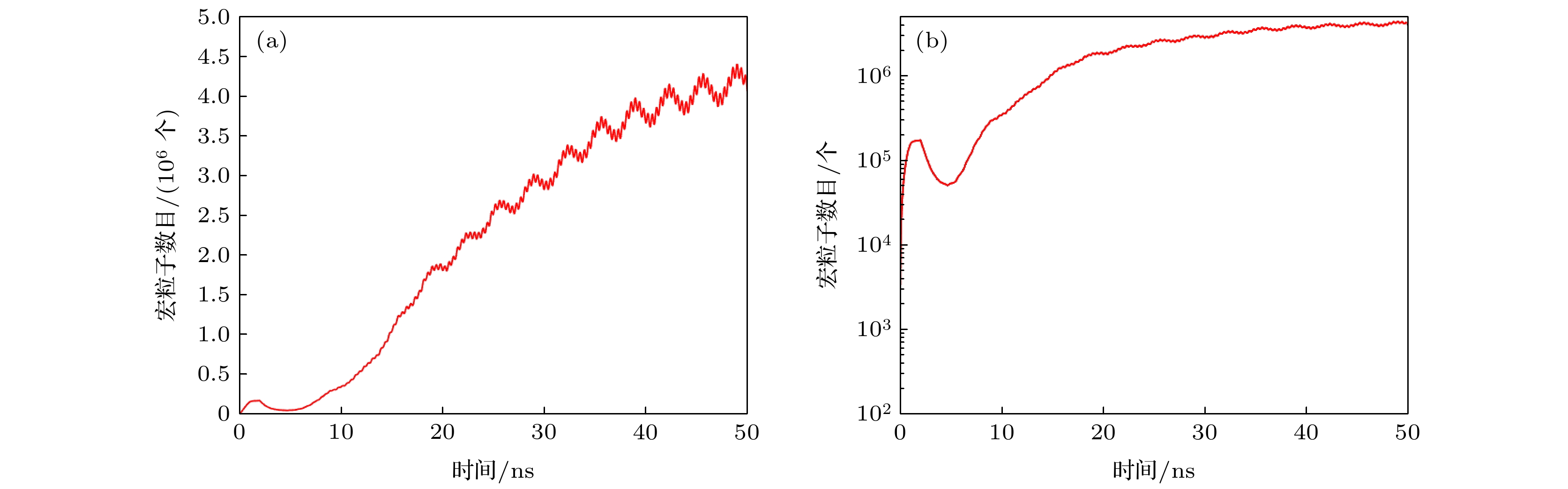
图 6 微放电过程中宏粒子数量随时间的变化 (a)纵轴为线性坐标; (b)纵轴为对数坐标
Figure 6. Accumulation of electrons during multipactions: (a) Vertical axis is linear; (b) vertical axis is logarithmic.

图 7 微放电过程中宏粒子的空间分布(侧视图) (a) 2 ns; (b) 20 ns; (c) 30 ns; (d) 293 ns
Figure 7. Distribution of space electrons accumulated at different times during a multipactor (side view): (a) 2 ns; (b) 20 ns; (c) 30 ns; (d) 293 ns.
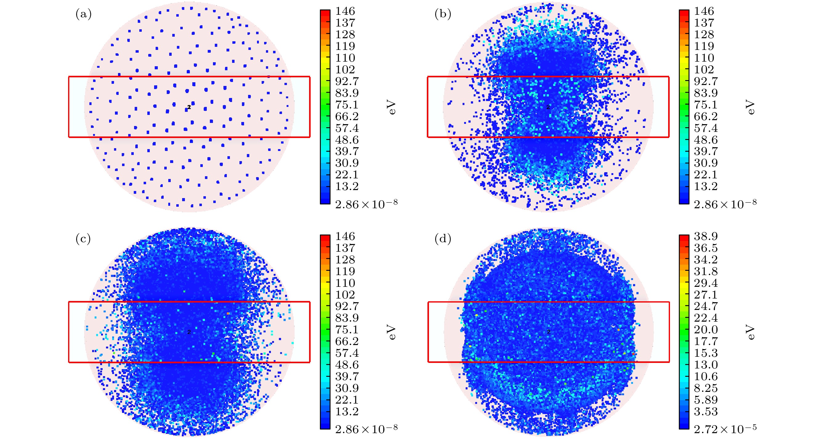
图 8 微放电过程中宏粒子的空间分布(正视图) (a) 2 ns; (b) 20 ns; (c) 30 ns; (d) 293 ns
Figure 8. Distribution of space electrons accumulated at different times during a multipactor (front view): (a) 2 ns; (b) 20 ns; (c) 30 ns; (d) 293 ns.

图 9 微放电过程中介质表面累积电荷密度的变化(颜色标尺是对数显示) (a) 2 ns; (b) 20 ns; (c) 30 ns; (d) 293 ns
Figure 9. Distribution of surface charge density accumulated during the multipactor (the color scaling is in logarithmic): (a) 2 ns; (b) 20 ns; (c) 30 ns; (d) 293 ns.
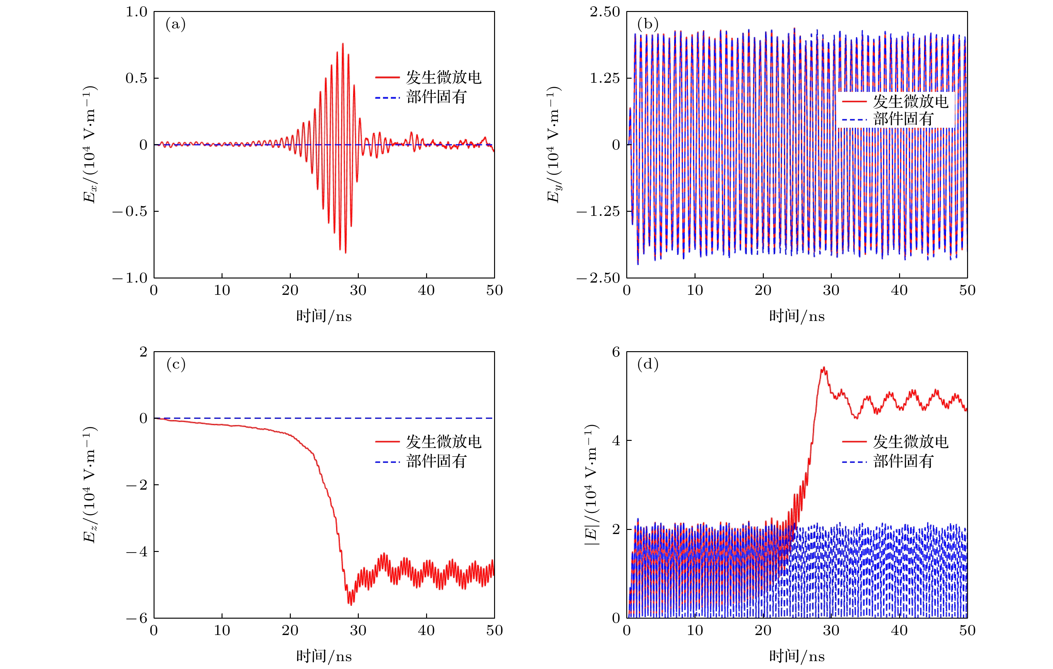
图 10 微放电过程中介质表面电场强度的变化 (a) Ex; (b) Ey; (c) Ez; (d) |E |
Figure 10. Variation of the surface electric field intensity during the multipaction: (a) Ex; (b) Ey; (c) Ez; (d) |E |
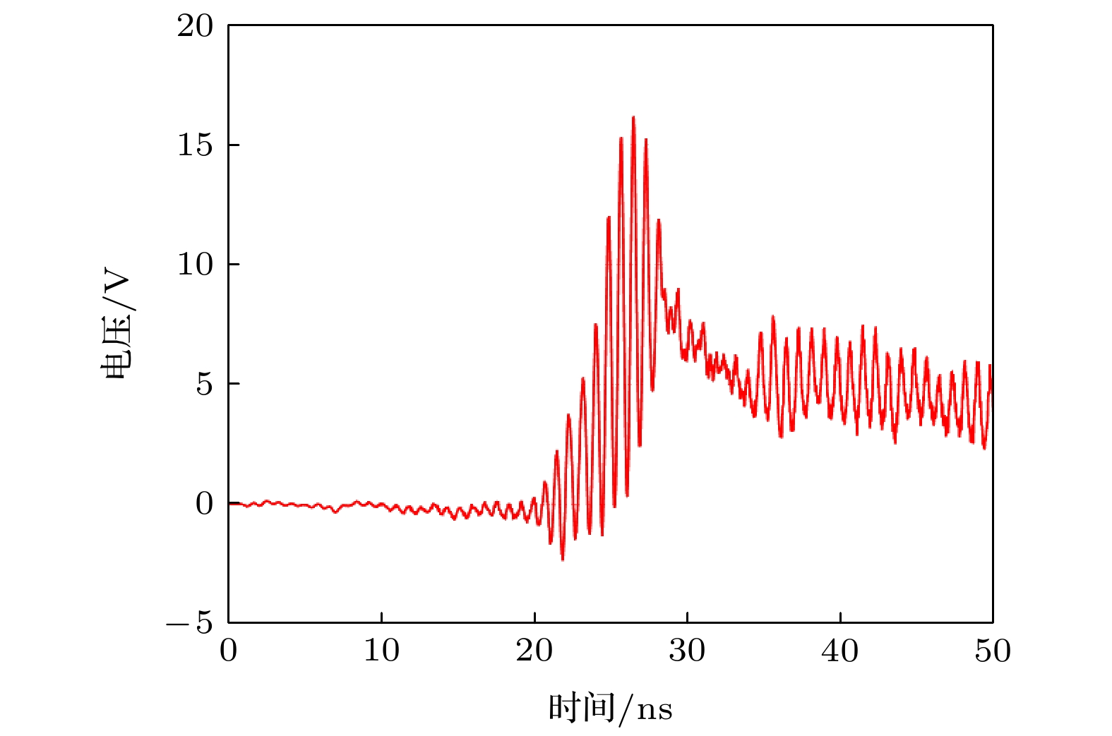
图 11 微放电过程中介质表面中心点处电压的变化
Figure 11. Variation of the surface voltage of dielectric during the multipactor.
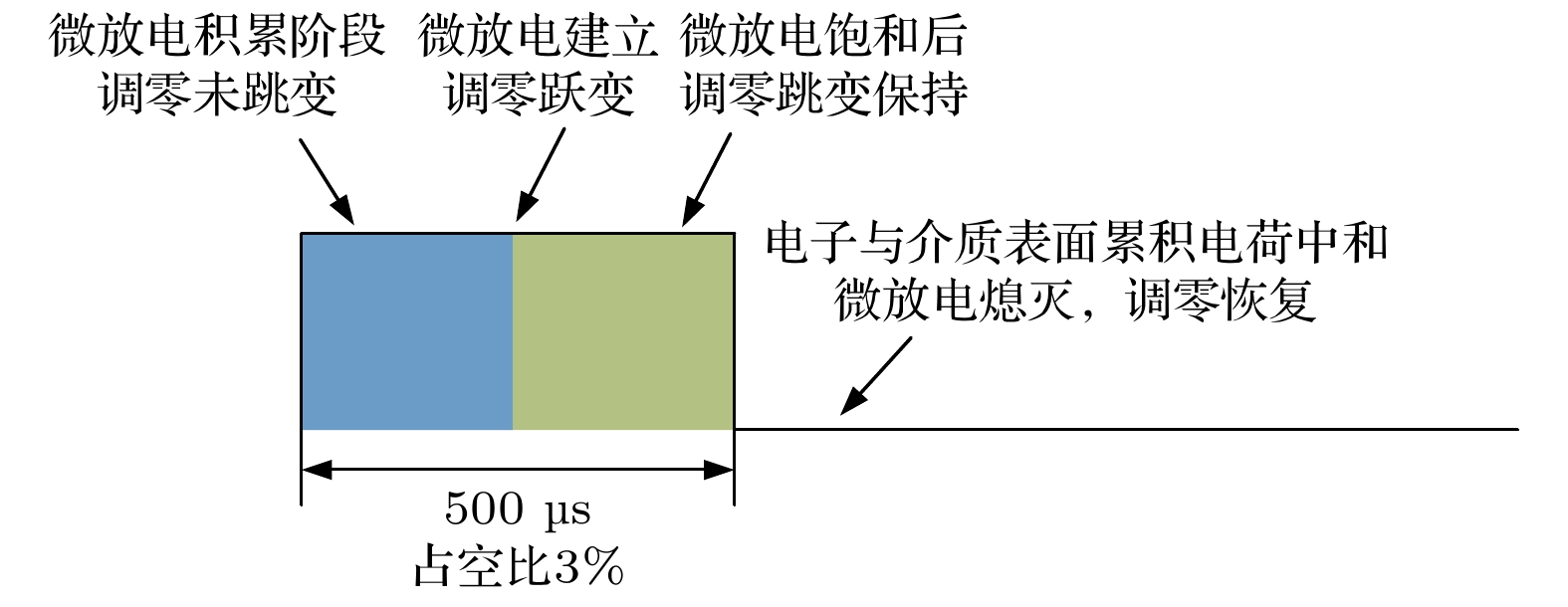
图 12 实验用脉冲信号
Figure 12. Pulse signal used in the multipactor test.
-
[1] Woode A, Petit J 1990 ESA J. 14 467
Google Scholar
[2] Rozario N, Lenzing H F, Reardon K F, Zarro M S, Baran C G 1994 IEEE Trans. Microwave Theory Tech. 42 558
Google Scholar
[3] Yu M 2007 IEEE Microwave Mag. 8 88
Google Scholar
[4] Kishek R A, Lau Y Y, Ang L K, Valfells A, Gilgenbach, R M 1998 Phys. Plasmas 5 2120
Google Scholar
[5] Kishek R A, Lau Y Y 1998 Phys. Rev. Lett. 80 193
Google Scholar
[6] Chang C, Liu G, Tang C, Chen C, Fang J 2011 Phys. Plasmas 18 055702
Google Scholar
[7] Hatch A J 1966 Nucl. Instrum. Methods 41 261
Google Scholar
[8] Power J G, Gai W, Gold S H, et al. 2004 Phys. Rev. Lett. 92 164801
Google Scholar
[9] Neuber A, Hemmert D, Krompholz H, et al. 1999 J. Appl. Phys. 86 1724
Google Scholar
[10] Chang C, Zhu M, Verboncoeur J, et al. 2014 Appl. Phys. Lett. 104 253504
Google Scholar
[11] Iqbal A, Wong P Y, Wen D Q, et al. 2020 Phys. Rev. E 102 043201
Google Scholar
[12] Neuber A, Butch M, Krompholz H, et al. 2000 IEEE Trans. Plasma Sci. 28 1593
Google Scholar
[13] Anderson R B, Getty W D, Brake M L, et al. 2001 Rev. Sci. Instrum. 72 3095
Google Scholar
[14] Ang L K, Lau Y Y, Kishek R A, Gilgenbach R M 1998 IEEE Trans. Plasma Sci. 26 290
Google Scholar
[15] Kim H C, Verboncoeur J P 2005 Phys. Plasmas 12 123504
Google Scholar
[16] Sazontov A, Semenov V, Buyanova M, et al. 2005 Phys. Plasmas 12 093501
Google Scholar
[17] Shen F Z, Wang X B, Cui W Z, Ran L X 2020 IEEE Trans. Plasma Sci. 48 433
Google Scholar
[18] Zhang Z Y, Sun Y Z, Cui W Z, et al. 2019 IEEE Trans. Electron Devices 66 4921
Google Scholar
[19] 董烨, 董志伟, 杨温渊, 周前红, 周海京 2013 62 197901
Google Scholar
Dong Y, Dong Z W, Yang W Y, Zhou Q H, Zhou H J 2013 Acta Phys. Sin. 62 197901
Google Scholar
[20] 张雪, 王勇, 范俊杰, 张瑞 2014 63 227901
Google Scholar
Zhang X, Wang Y, Fan J J, Zhang R 2014 Acta Phys. Sin. 63 227901
Google Scholar
[21] Langellotti S V, Jordan N M, Lau Y Y, et al. 2020 IEEE Trans. Plasma Sci. 48 1942
Google Scholar
[22] Hemmert D, Neuber A, Dickens J, et al. 2000 IEEE Trans. Plasma Sci. 28 472
Google Scholar
[23] Vaughan J R M 1988 IEEE Trans. Electron Devices 35 1172
Google Scholar
[24] Wang X B, Shen J H, Wang J Y, et al. 2017 IEEE Trans. Microwave Theory Tech. 65 2734
Google Scholar


 DownLoad:


Catalog
Metrics
- Abstract views: 6570
- PDF Downloads: 63
- Cited By: 0
