-
CdZnTe recently emerged as a leading semiconductor crystal for fabricating room-temperature x- and gamma-ray imaging detectors, due to its excellent energy resolution and sensitivity. However, its wide deployment is hampered by the low availability of high-quality CdZnTe crystals. As-grown CdZnTe crystals generally encounter the problems arising from the impurities and defects, especially deep level defects. The presence of impurities and defects leads to severe charge trapping, which significantly affects detector performance. Especially for high counting rate imaging detector used in medical imaging and tomography, the accumulation of space charge at deep levels significantly deforms the electric field distribution and subsequently reduces the charge collection efficiency. Therefore, a considerable interest is focused on the investigation of the space charge accumulation effect in CdZnTe crystal, which is the key factor to improve the performance of high counting rate imaging detector. Thus, the goal of this work is to investigate the effects of deep level defects on space charge distribution and internal electric field in CdZnTe detector. In order to reveal the major problem therein, Silvaco TCAD technique is used to simulate the space charge and electric field distribution profile in CdZnTe detector with considering the typical deep level defects
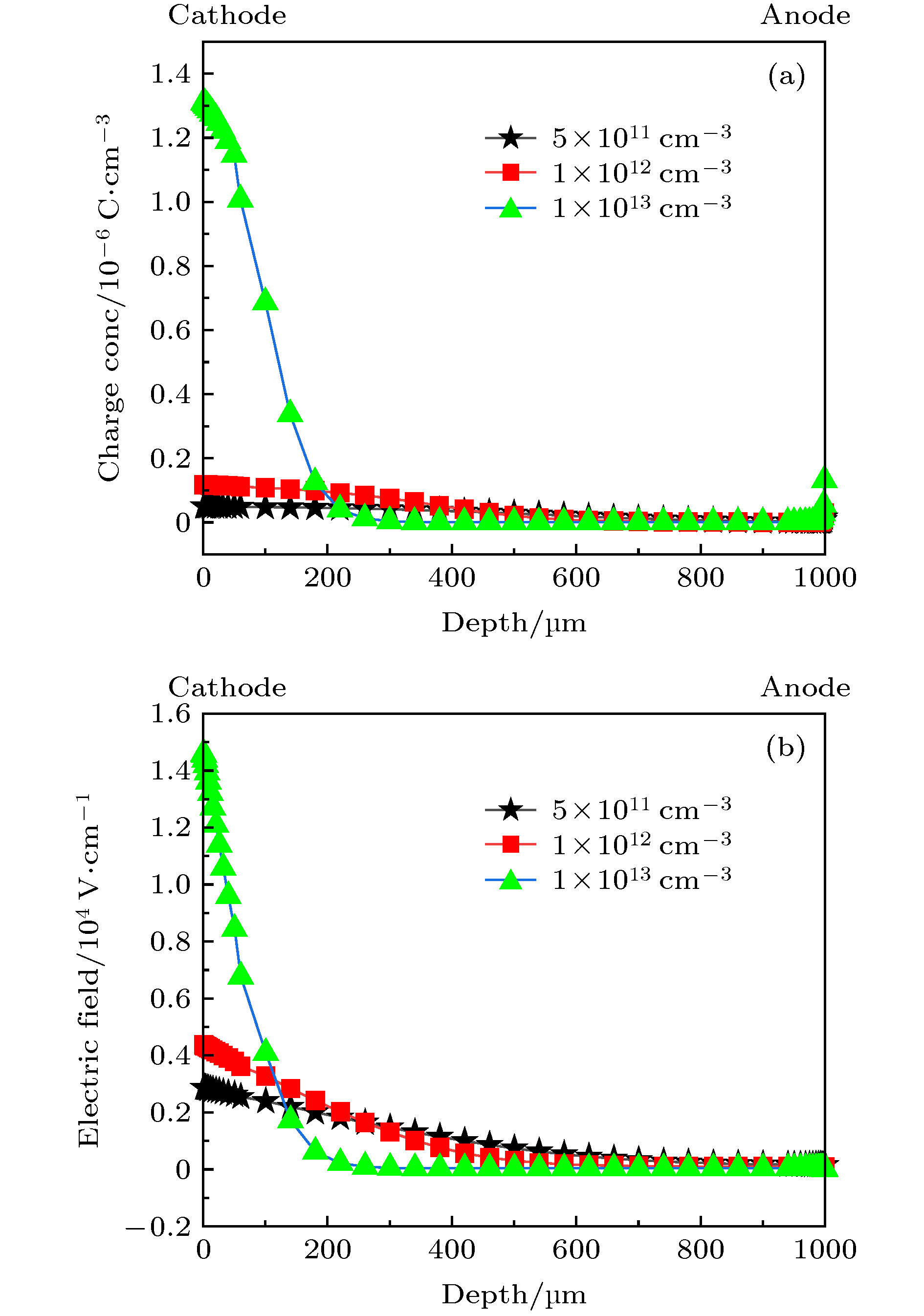
$ \rm Te_{Cd}^{++} $ in CdZnTe crystals with activation energy of Ev + 0.86 eV and concentration of 1 × 1012 cm–3 at room temperature. The simulation results demonstrate that the Au/ CdZnTe /Au energy band tilts intensively with the increase of applied bias, which makes the deep level ionization fraction increase. The space charge concentration also increases in the crystal. Meanwhile, the dead layer of electric field distribution decreases, which is of benefit to the carrier collection of CdZnTe detector. In addition, under the premiseof the high resistivity of CdZnTe crystal, the reduction of deep level defect concentration located at Ev + 0.86 eV can narrow the internal dead layer moderately. The deep level defect located at Ev + 0.8 eV can also reduce the space charge concentration near the cathode, which flattens the electric field distribution with narrower dead layer, thus significantly improving the carrier collection efficiency of CdZnTe detector. These simulation results will provide meaningful theoretical guidance for further optimizing the CdZnTe crystal growth, device design and fabrication.-
Keywords:
- CdZnTe nuclear radiation detector /
- space charge /
- deep level defect /
- charge collection efficiency
[1] Czyz S A, Farsoni A T, Gadey H R 2019 Nucl. Instrum. Methods Phys. Res., Sect. A 945 162614
 Google Scholar
[2] Johns P M, Nino J C 2019 J. Appl. Phys. 126 040902
 Google Scholar
[3] Guo Q, Beilicke M, Garson A, Kislat F, Fleming D, Krawczynski H 2012 Astropart. Phys. 41 63
 Google Scholar
[4] Prokesch M, Soldner S A, Sundaram A G, Reed M D, Li H, Eger J F, Reiber J L, Shanor C L, Wray C L, Emerick A J, Peters A F, Jones C L 2016 IEEE Trans. Nucl. Sci. 63 1854
 Google Scholar
[5] Chai L, Chen L, Yang C P, Zhou D D, Yang M M, Qu W W, Zhang G L, Hei D Q, Xu S P, Chen X J 2019 Nucl. Sci. Tech. 30 91
 Google Scholar
[6] Jiang W, Chalich Y, Deen M J 2019 Sensors 19 5019
 Google Scholar
[7] Iniewski K 2014 J. Instrum. 9 C11001
 Google Scholar
[8] Carvalho A, Tagantsev A K, Öberg S, Briddon P R, Setter N 2010 Phys. Rev. B 81 075215
 Google Scholar
[9] Chu M, Terterian S, Ting D, Wang C C, Gurgenian H K, Mesropian S 2001 Appl. Phys. Lett. 79 2728
 Google Scholar
[10] Szeles C, Shan Y, Lynn K G, Moodenbaugh A, Eissler E E 1997 Phys. Rev. B 55 6945
 Google Scholar
[11] Bale D S, Szeles C 2008 Phys. Rev. B 77 035205
 Google Scholar
[12] Soldner S A, Bale D S, Szeles C 2007 IEEE Trans. Nucl. Sci. 54 1723
 Google Scholar
[13] Cola A, Farella I 2013 Sensors 13 9414
 Google Scholar
[14] Li Y, Zha G, Guo Y, Xi S, Xu L, Jie W 2020 Sensors 20 383
 Google Scholar
[15] Bale D S, Soldner S A, Szeles C 2008 Appl. Phys. Lett. 92 082101.1
 Google Scholar
[16] Camarda G S, Bolotnikov A E, Cui Y, Hossain A, Awadalla S A, Mackenzie J, Chen H, James R B 2007 IEEE Nuclear Science Symposium Conference Record Honolulu, Hawaii, USA, October 26 – November 3, 2007 p1798
[17] Musiienko A, Grill R, Pekárek J, Belas E, Praus P, Pipek J, Dědič V, Elhadidy H 2017 Appl. Phys. Lett. 111 082103.1
 Google Scholar
[18] Mahmood S A 2019 J. Appl. Phys. 125 214505
 Google Scholar
[19] Thomas B, Veale M C, Wilson M D, Seller P, Schneider A, Iniewski K 2017 J. Instrum. 12 C12045
 Google Scholar
[20] Maneuski D, Gostilo V, Owens A 2019 J. Phys. D: Appl. Phys. 53 015114
 Google Scholar
[21] Das A, Duttagupta S P 2015 Radiat.Prot. Dosim. 167 443
 Google Scholar
[22] Johannesson D, Nawaz M, Nee H P 2019 Mater. Sci. Forum. 963 670
 Google Scholar
[23] 唐龙谷 2014 半导体工艺和器件仿真软件Silvaco TCAD实用教程 (北京: 清华大学出版社) 第99页
Tang L G 2014 Semiconductor Process and Device Simulation Software Silvaco TCAD Practical Tutorial (Beijing: Tsinghua University Press) p99 (in Chinese)
[24] Prokesch M, Szeles C 2007 Phys. Rev. B 75 245204.1
 Google Scholar
[25] Gul R, Roy U N, James R B 2017 J. Appl. Phys. 121 115701.1
 Google Scholar
[26] Simmons J G, Taylor G W 1971 Phys. Rev. B 4 502
 Google Scholar
-
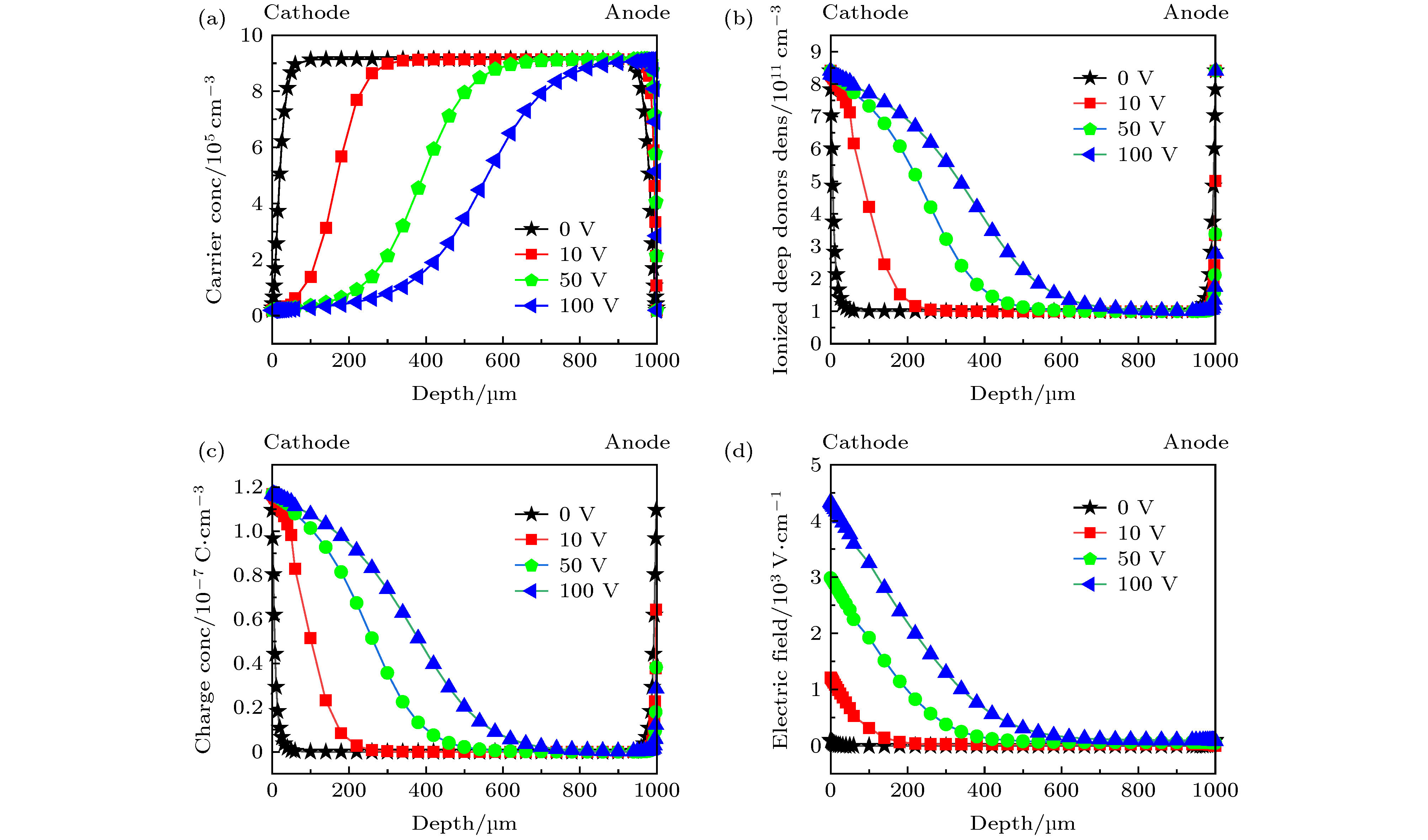
图 2 不同偏压下的Au/CdZnTe/Au器件仿真结果 (a) 载流子浓度分布; (b) 深施主的电离浓度分布; (c) 空间电荷浓度分布; (d) 内部电场强度分布变化规律
Figure 2. Simulation results of Au/CdZnTe/Au device under different bias voltages: (a) Distribution of carrier concentration; (b) density of ionized deep donors; (c) distribution of space charge concentration; (d) distribution of internal electric field intensity.
图 3 Au/CdZnTe/Au器件内能带和内部电场分布示意图 (a) 热平衡的Au/CdZnTe/Au能带结构图; (b) U > 0的Au/CdZnTe/Au能带结构图; (c) 内部电场分布示意图
Figure 3. Energy-band diagram and internal electric field distribution in Au/CdZnTe/Au device: (a) Au/CdZnTe/Au energy-band diagram in thermal equilibrium; (b) Au/CdZnTe/Au energy-band diagram under U > 0; (c) schematic diagram of internal electric field distribution.
表 1 CdZnTe晶体的基本参数
Table 1. Basic parameters of CdZnTe crystals.
介电常数 300 K时禁带宽度/eV 300 K时导带密度/cm–3 300 K时价带密度/cm–3 电子迁移率/ cm2·V–1·s–1 空穴迁移率/cm2·V–1·s–1 10.9 1.6 9.14 × 10¹⁷ 5.19 × 10¹⁸ 1000 100 表 2 深施主能级的基本信息
Table 2. Basic information of deep donor energy levels.
类型 位置/eV 浓度/cm–3 电子俘获界面/cm2 空穴俘获界面/cm2 简并度 Donor1 Ev + 0.86 5 × 10¹² 3 × 10–14 3 × 10–15 2 Donor2 Ev + 0.86 1 × 10¹² 3 × 10–14 3 × 10–15 2 Donor3 Ev + 0.86 1 × 10¹³ 3 × 10–14 3 × 10–15 2 表 3 不同深能级缺陷浓度下CdZnTe晶体的电阻率仿真结果
Table 3. The resistivity of CdZnTe crystals at different deep energy level concentrations via simulation.
能级类型 位置/eV 浓度/cm–3 电阻率/Ω·cm 无深施主能级 — — 6.08 × 10⁵ Donor1 Ev + 0.86 5 × 10¹¹ 1.50 × 10¹⁰ Donor2 Ev + 0.86 1 × 10¹² 6.66 × 10⁹ Donor3 Ev + 0.86 1 × 10¹³ 6.05 × 10⁸ -
[1] Czyz S A, Farsoni A T, Gadey H R 2019 Nucl. Instrum. Methods Phys. Res., Sect. A 945 162614
 Google Scholar
[2] Johns P M, Nino J C 2019 J. Appl. Phys. 126 040902
 Google Scholar
[3] Guo Q, Beilicke M, Garson A, Kislat F, Fleming D, Krawczynski H 2012 Astropart. Phys. 41 63
 Google Scholar
[4] Prokesch M, Soldner S A, Sundaram A G, Reed M D, Li H, Eger J F, Reiber J L, Shanor C L, Wray C L, Emerick A J, Peters A F, Jones C L 2016 IEEE Trans. Nucl. Sci. 63 1854
 Google Scholar
[5] Chai L, Chen L, Yang C P, Zhou D D, Yang M M, Qu W W, Zhang G L, Hei D Q, Xu S P, Chen X J 2019 Nucl. Sci. Tech. 30 91
 Google Scholar
[6] Jiang W, Chalich Y, Deen M J 2019 Sensors 19 5019
 Google Scholar
[7] Iniewski K 2014 J. Instrum. 9 C11001
 Google Scholar
[8] Carvalho A, Tagantsev A K, Öberg S, Briddon P R, Setter N 2010 Phys. Rev. B 81 075215
 Google Scholar
[9] Chu M, Terterian S, Ting D, Wang C C, Gurgenian H K, Mesropian S 2001 Appl. Phys. Lett. 79 2728
 Google Scholar
[10] Szeles C, Shan Y, Lynn K G, Moodenbaugh A, Eissler E E 1997 Phys. Rev. B 55 6945
 Google Scholar
[11] Bale D S, Szeles C 2008 Phys. Rev. B 77 035205
 Google Scholar
[12] Soldner S A, Bale D S, Szeles C 2007 IEEE Trans. Nucl. Sci. 54 1723
 Google Scholar
[13] Cola A, Farella I 2013 Sensors 13 9414
 Google Scholar
[14] Li Y, Zha G, Guo Y, Xi S, Xu L, Jie W 2020 Sensors 20 383
 Google Scholar
[15] Bale D S, Soldner S A, Szeles C 2008 Appl. Phys. Lett. 92 082101.1
 Google Scholar
[16] Camarda G S, Bolotnikov A E, Cui Y, Hossain A, Awadalla S A, Mackenzie J, Chen H, James R B 2007 IEEE Nuclear Science Symposium Conference Record Honolulu, Hawaii, USA, October 26 – November 3, 2007 p1798
[17] Musiienko A, Grill R, Pekárek J, Belas E, Praus P, Pipek J, Dědič V, Elhadidy H 2017 Appl. Phys. Lett. 111 082103.1
 Google Scholar
[18] Mahmood S A 2019 J. Appl. Phys. 125 214505
 Google Scholar
[19] Thomas B, Veale M C, Wilson M D, Seller P, Schneider A, Iniewski K 2017 J. Instrum. 12 C12045
 Google Scholar
[20] Maneuski D, Gostilo V, Owens A 2019 J. Phys. D: Appl. Phys. 53 015114
 Google Scholar
[21] Das A, Duttagupta S P 2015 Radiat.Prot. Dosim. 167 443
 Google Scholar
[22] Johannesson D, Nawaz M, Nee H P 2019 Mater. Sci. Forum. 963 670
 Google Scholar
[23] 唐龙谷 2014 半导体工艺和器件仿真软件Silvaco TCAD实用教程 (北京: 清华大学出版社) 第99页
Tang L G 2014 Semiconductor Process and Device Simulation Software Silvaco TCAD Practical Tutorial (Beijing: Tsinghua University Press) p99 (in Chinese)
[24] Prokesch M, Szeles C 2007 Phys. Rev. B 75 245204.1
 Google Scholar
[25] Gul R, Roy U N, James R B 2017 J. Appl. Phys. 121 115701.1
 Google Scholar
[26] Simmons J G, Taylor G W 1971 Phys. Rev. B 4 502
 Google Scholar
Catalog
Metrics
- Abstract views: 10365
- PDF Downloads: 237
- Cited By: 0


 DownLoad:


