-
无铅 K1–xNaxNbO3 薄膜作为传感器以及机电和电卡冷却装置的候选者越来越受到关注. 但是(111)取向K1–xNaxNbO3薄膜的相变与电卡效应的内在关联还并不清楚. 本文首先推导出基于八阶朗道自由能多项式的(111)取向铁电薄膜的热力学势, 并在此基础上建立了K0.5Na0.5NbO3薄膜温度-错配应变相图和室温错配应变-面外应力相图. 重点研究了(111)取向K0.5Na0.5NbO3 薄膜的室温电卡效应的应变和取向控制, 这对于实际的电卡制冷应用至关重要. 研究发现, 在无面外应力和零错配应变下, 三方铁电-顺电相变附近, 30 MV/m电场下K0.5Na0.5NbO3薄膜在居里温度附近(约673 K)最大电卡绝热温变 ΔT 可高达18 K. 施加约–6.7 GPa 的面外应力可以有效地将居里温度降低至室温, 但代价是最大绝热温变ΔT降低至7.5 K. 本工作为应变和取向工程调控 K1–xNaxNbO3基薄膜的相变和电卡性能提供了理论指导.Lead-free K1–xNaxNbO3 thin films, as a candidate for sensors and electromechanical and electrocaloric cooling devices, have increasingly received attention. However, for (111)-oriented films, the relation between phase transitions and electrocaloric effect is not clear. Here, we derive the thermodynamic potential of (111)-oriented thin film ferroelectrics K1–xNaxNbO3 based on the 8th order polynomial function, and then establish the temperature-misfit strain and out-of-plane stress-in-plane misfit strain phase diagrams and calculate electrocaloric (EC) entropy changes ΔS and temperature changes ΔT. This study focuses on mechanical and orientation controls of room-temperature EC effect of K0.5Na0.5NbO3 films, which is critical for environmentally friendly electrocaloric refrigeration applications in practice. Under the stress-free and zero misfit strain conditions, the (111)-oriented K0.5Na0.5NbO3 film in an electric field of 30 MV/m has a maximum EC ΔT of ~18 K near the rhombohedral ferroelectric-paraelectric phase transition temperature (about 673 K). However, an out-of-plane stress of about –6.7GPa can reduce the optimal operating temperature to room temperature where the K0.5Na0.5NbO3 film has the EC ΔT of ~7.5 K under the action of applied electric field of 30 MV/m. The present work provides theoretical guidance for exploring the strain engineering and orientation engineering of K1–xNaxNbO3-based thin films with optimized electrocaloric and electromechanical properties.
-
Keywords:
- ferroelectric film /
- electrocaloric /
- orientation /
- strain
[1] Moya X, Kar-Narayan S, Mathur N 2014 Nat. Mater. 13 439
 Google Scholar
[2] Mischenko A, Zhang Q, Scott J, Whatmore R, Mathur N 2006 Science 311 1270
 Google Scholar
[3] Shi J, Han D, Li Z, et al. 2019 Joule 3 1200
 Google Scholar
[4] Meng Y, Pu J, Pei Q 2021 Joule 5 780
 Google Scholar
[5] Torello A, P. Lheritier P, Usui T, et al. 2020 Science 370 125
 Google Scholar
[6] Wang Y, Zhang Z, Usui T, et al. 2020 Science 370 129
 Google Scholar
[7] Nair B, Usui T, Crossley S, et al. 2019 Nature 33 468
[8] Yasuyoshi S, Hisaaki T, Toshihiko T, Tatsuhiko N, Kazumasa T, Takahiko H, Toshiatsu N, Masaya N 2004 Nature 432 84
 Google Scholar
[9] Shrout T, Zhang S 2007 J. Electroceram. 19 185
 Google Scholar
[10] Zhang M, Wang K, Du Y, Dai G, Sun W, Li G, Hu D, Thong H, Zhao C, Xi X, Yue Z, Li J 2017 J. Am. Chem. Soc. 139 3889
 Google Scholar
[11] Li J, Wang K, Zhu F, Cheng L, Yao F 2013 J. Am. Ceram. Soc. 96 3677
 Google Scholar
[12] Gupta A, Kumar R, Singh S 2018 Scr. Mater. 143 5
 Google Scholar
[13] Wang X, Wu J, Dkhil B, Xu B, Wang X, Dong G, Yang G, Lou X 2017 Appl. Phys. Lett. 110 063904
 Google Scholar
[14] Zhao X, Wang J, Chen L 2020 Appl. Phys. Lett. 116 092902
 Google Scholar
[15] Pertsev N, Zembilgotov A, Tagantsev A 1998 Phys. Rev. Lett. 80 1988
 Google Scholar
[16] Bai G, Ma W 2010 Physica B 405 190
 Google Scholar
[17] 刘迪, 王静, 王俊升, 黄厚兵 2020 69 127801
 Google Scholar
Liu D, Wang J, Wang J S, Huang H B 2020 Acta Phys. Sin. 69 127801
 Google Scholar
[18] 高荣贞, 王静, 王俊升, 黄厚兵 2020 69 217801
 Google Scholar
Gao R, Wang J, Wang J, Huang H 2020 Acta Phys. Sin. 69 217801
 Google Scholar
[19] Zhou M, Wang J, Chen L, Nan C 2018 J. Appl. Phys. 123 154106
 Google Scholar
[20] Bai G, Qin K, Xie Q, Yan X, Gao C, Liu Z 2017 Mater. Lett. 186 146
 Google Scholar
[21] Pohlmann H, Wang J, Wang B, Chen L 2017 Appl. Phys. Lett. 110 102906
 Google Scholar
[22] Wang J, Fortino D, Wang B, Zhao X, Chen L 2020 Adv. Mater. 32 1906224
 Google Scholar
[23] Gao R, Shi X, Wang J, Zhang G, Huang H 2021 Adv. Funct. Mater. 31 2104393
 Google Scholar
[24] Bai G, Xie Q, Liu Z, Wu D 2015 J. Appl. Phys. 118 074101
 Google Scholar
[25] Shan D, Lei C, Cai Y, et al. 2021 Int. J. Solids Struct. 216 59
 Google Scholar
[26] Harrington S, Zhai J, Denev S, et al. 2011 Nat. Nanotechnol. 6 491
 Google Scholar
[27] Emelyanov A, Pertsev N, Kholkin A 2002 Phys. Rev. B 66 214108
 Google Scholar
[28] Sun X, Huang H, Wang J, Wen Y, Dang Z 2019 J. Alloys. Compd. 777 821
 Google Scholar
[29] Liu D, Bai G, Gao C 2020 J. Appl. Phys. 127 154101
 Google Scholar
[30] 白刚, 林翠, 刘端生, 许杰, 李卫, 高存法 2021 70 127701
 Google Scholar
Bai G, Lin C, Liu D S, Xu J, Li W, Gao C F 2021 Acta Phys. Sin. 70 127701
 Google Scholar
[31] Peng B, Zhang Q, Gang B, et al. 2019 Energy Environ. Sci. 12 1708
 Google Scholar
[32] Tagantsev A, Pertsev N, Muralt P, Setter N 2001 Phys. Rev. B 65 012104
 Google Scholar
[33] Akcay G, Misirlioglu I B, Alpay S P 2006 Appl. Phys. Lett. 89 042903
 Google Scholar
[34] Zhang J X, Li Y L, Wang Y, Liu Z K, Chen L Q 2007 J. Appl. Lett. 101 114105
[35] Wu H, Ma X, Zhang Z, Zeng J, Wang J, Chai G 2016 AIP Adv. 6 015309
 Google Scholar
[36] Li C, Huang Y, Wang J, et al. 2021 Npj Comput. Mater. 7 1
 Google Scholar
[37] Valant M 2012 Prog. Mater. Sci. 57 980
 Google Scholar
[38] Liu Y, Scott J, Dkhil B 2016 Appl. Phys. Rev. 3 031102
 Google Scholar
-
图 1 (111)取向K0.5Na0.5NbO3薄膜的热力学计算结果 (a) 温度-失配应变相图和(b) 没有外加电场的薄膜极化分布; 薄膜在20 MV/m 的电场下的(c)极化分布、(d)极化变化分布、(e)电卡熵变化ΔS和(f)电卡温度变化ΔT. 粗线和细线分别表示一阶和二阶相变
Fig. 1. Thermodynamic calculated results for (111)-oriented K0.5Na0.5NbO3 films: (a) The temperature-misfit strain phase diagram and (b) the distribution of polarization without electric field; (c) the distribution of polarization, (d) the distribution of polarization change, (e) the electrocaloric (EC) entropy change ΔS, and (f) the EC temperature change ΔT with temperature and misfit strain for (111)-oriented K0.5Na0.5NbO3 films under the electric field of 20 MV/m. Thick and thin lines denote the first-order and second-order phase transitions, respectively.
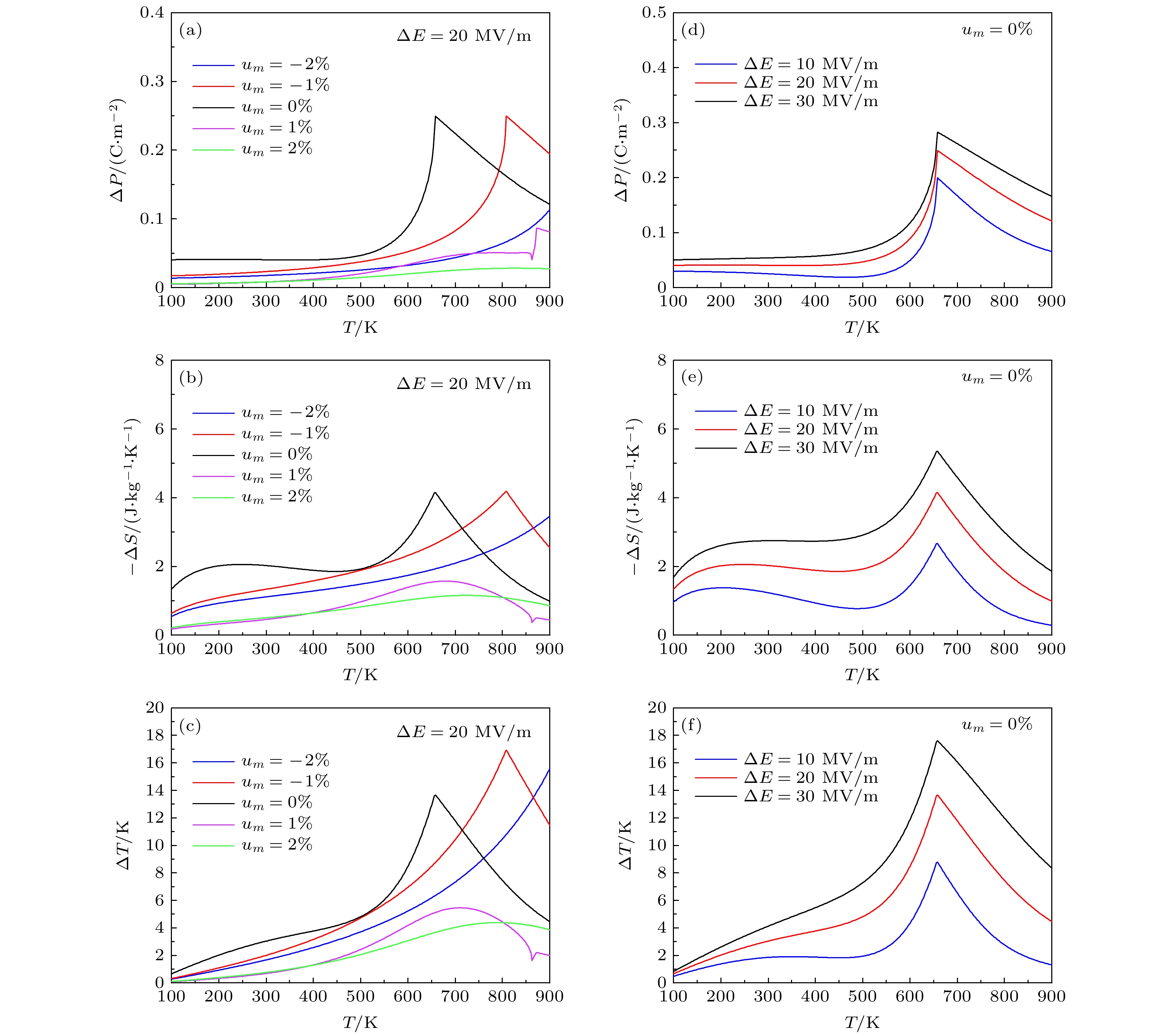
图 2 (a)—(c)在ΔE = 20 MV/m, 不同应变下, (111)取向K0.5Na0.5NbO3薄膜的极化变化、电卡 ΔS和电卡ΔT随温度的变化; (d)—(f)在um = 0, 不同电场下, (111)取向K0.5Na0.5NbO3薄膜的极化变化、电卡ΔS和电卡ΔT随温度的变化
Fig. 2. Polarization changes, the EC entropy change ΔS and the EC temperature change ΔT change with temperature for (111)-oriented K0.5Na0.5NbO3 films: (a)–(c) Under different strains at ΔE = 20 MV/m; (d)–(f) under different electric fields and strain-free conditions.
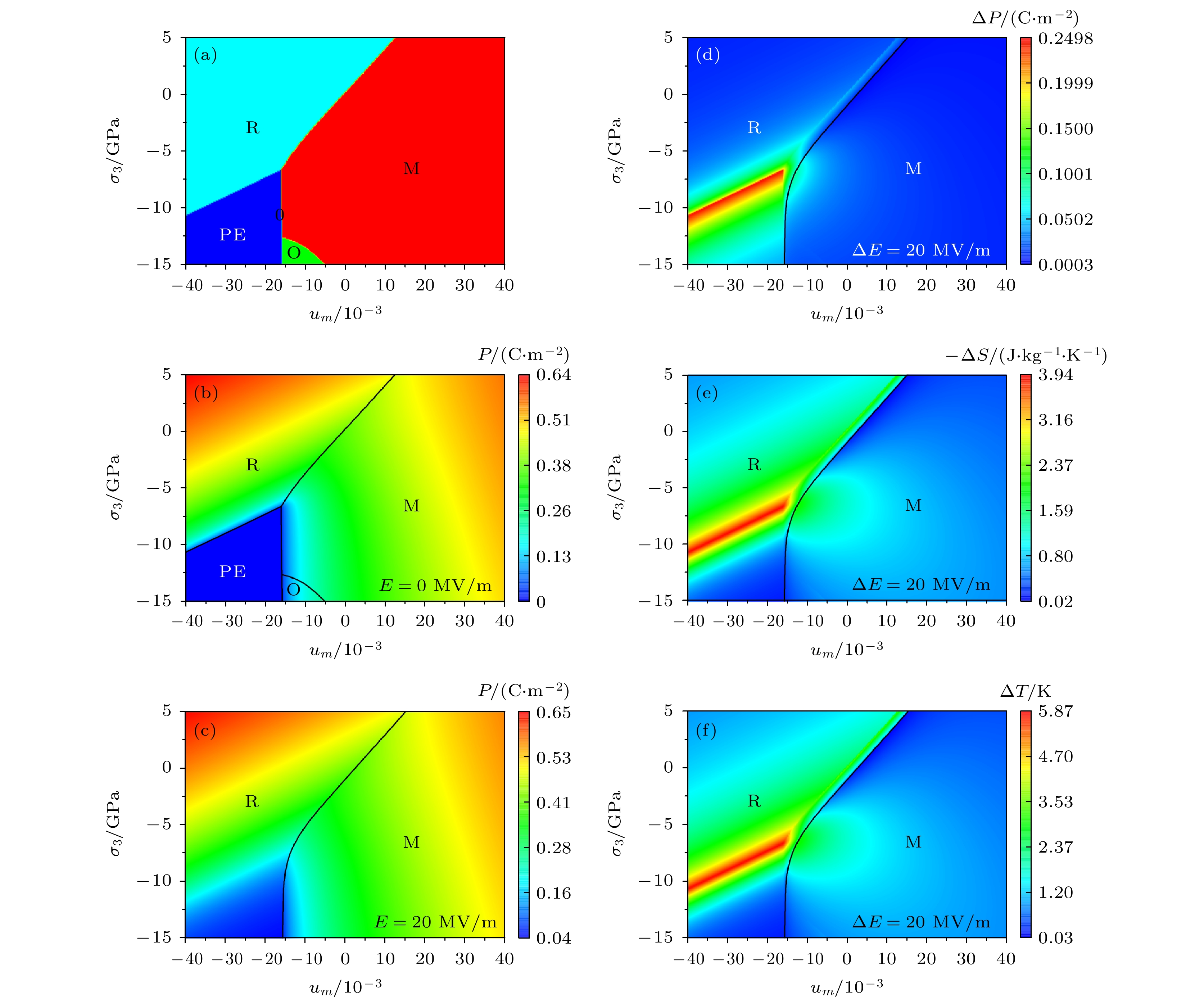
图 3 室温下(111)取向K0.5Na0.5NbO3薄膜的热力学计算结果 (a) 面外应力-面内错配应变相图和(b)没有电场的极化分布; 电场20 MV/m下, (c)极化、(d)极化变化、(e)电卡ΔS和(f)电卡ΔT在相图中的分布
Fig. 3. Thermodynamic calculated results for (111)-oriented K0.5Na0.5NbO3 films: (a) Out-of-plane stress- misfit strain phase diagram and (b) the distribution of polarization without electric field; (c) the distribution of polarization, (d) polarization change, (e) the EC entropy change ΔS, and (f) the EC temperature change ΔT with external stress and misfit strain under the electric field of 20 MV/m at room temperature (298 K). Thick and thin lines denote the first-order and second-order phase transitions, respectively.
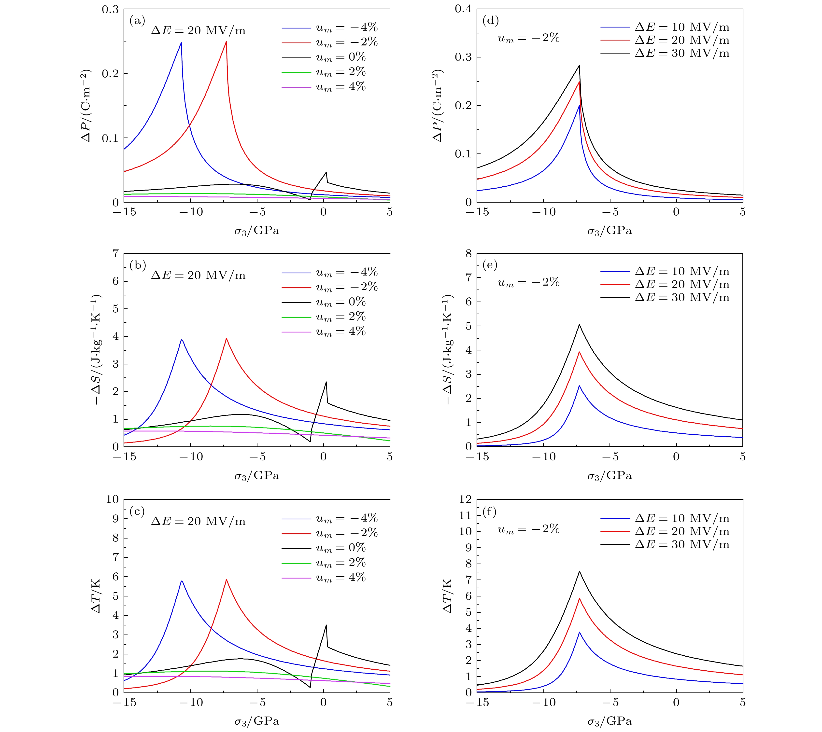
图 4 (a)—(c)在ΔE = 20 MV/m, 不同错配应变下(111)取向K0.5Na0.5NbO3薄膜的极化变化、电卡ΔS和电卡ΔT随面外应力的变化; (d)—(f)在um = –0.02, 不同电场下, (111)取向K0.5Na0.5NbO3薄膜的极化变化、电卡 ΔS和电卡ΔT随面外应力的变化
Fig. 4. Polarization changes, the EC entropy change ΔS and the EC temperature change ΔT change with out-of-plane stress for (111)-oriented K0.5Na0.5NbO3 films: (a)–(c) Under different misfit strains at ΔE = 20 MV/m; (d)–(f) under different electric fields and the misfit strain of –0.02.
-
[1] Moya X, Kar-Narayan S, Mathur N 2014 Nat. Mater. 13 439
 Google Scholar
[2] Mischenko A, Zhang Q, Scott J, Whatmore R, Mathur N 2006 Science 311 1270
 Google Scholar
[3] Shi J, Han D, Li Z, et al. 2019 Joule 3 1200
 Google Scholar
[4] Meng Y, Pu J, Pei Q 2021 Joule 5 780
 Google Scholar
[5] Torello A, P. Lheritier P, Usui T, et al. 2020 Science 370 125
 Google Scholar
[6] Wang Y, Zhang Z, Usui T, et al. 2020 Science 370 129
 Google Scholar
[7] Nair B, Usui T, Crossley S, et al. 2019 Nature 33 468
[8] Yasuyoshi S, Hisaaki T, Toshihiko T, Tatsuhiko N, Kazumasa T, Takahiko H, Toshiatsu N, Masaya N 2004 Nature 432 84
 Google Scholar
[9] Shrout T, Zhang S 2007 J. Electroceram. 19 185
 Google Scholar
[10] Zhang M, Wang K, Du Y, Dai G, Sun W, Li G, Hu D, Thong H, Zhao C, Xi X, Yue Z, Li J 2017 J. Am. Chem. Soc. 139 3889
 Google Scholar
[11] Li J, Wang K, Zhu F, Cheng L, Yao F 2013 J. Am. Ceram. Soc. 96 3677
 Google Scholar
[12] Gupta A, Kumar R, Singh S 2018 Scr. Mater. 143 5
 Google Scholar
[13] Wang X, Wu J, Dkhil B, Xu B, Wang X, Dong G, Yang G, Lou X 2017 Appl. Phys. Lett. 110 063904
 Google Scholar
[14] Zhao X, Wang J, Chen L 2020 Appl. Phys. Lett. 116 092902
 Google Scholar
[15] Pertsev N, Zembilgotov A, Tagantsev A 1998 Phys. Rev. Lett. 80 1988
 Google Scholar
[16] Bai G, Ma W 2010 Physica B 405 190
 Google Scholar
[17] 刘迪, 王静, 王俊升, 黄厚兵 2020 69 127801
 Google Scholar
Liu D, Wang J, Wang J S, Huang H B 2020 Acta Phys. Sin. 69 127801
 Google Scholar
[18] 高荣贞, 王静, 王俊升, 黄厚兵 2020 69 217801
 Google Scholar
Gao R, Wang J, Wang J, Huang H 2020 Acta Phys. Sin. 69 217801
 Google Scholar
[19] Zhou M, Wang J, Chen L, Nan C 2018 J. Appl. Phys. 123 154106
 Google Scholar
[20] Bai G, Qin K, Xie Q, Yan X, Gao C, Liu Z 2017 Mater. Lett. 186 146
 Google Scholar
[21] Pohlmann H, Wang J, Wang B, Chen L 2017 Appl. Phys. Lett. 110 102906
 Google Scholar
[22] Wang J, Fortino D, Wang B, Zhao X, Chen L 2020 Adv. Mater. 32 1906224
 Google Scholar
[23] Gao R, Shi X, Wang J, Zhang G, Huang H 2021 Adv. Funct. Mater. 31 2104393
 Google Scholar
[24] Bai G, Xie Q, Liu Z, Wu D 2015 J. Appl. Phys. 118 074101
 Google Scholar
[25] Shan D, Lei C, Cai Y, et al. 2021 Int. J. Solids Struct. 216 59
 Google Scholar
[26] Harrington S, Zhai J, Denev S, et al. 2011 Nat. Nanotechnol. 6 491
 Google Scholar
[27] Emelyanov A, Pertsev N, Kholkin A 2002 Phys. Rev. B 66 214108
 Google Scholar
[28] Sun X, Huang H, Wang J, Wen Y, Dang Z 2019 J. Alloys. Compd. 777 821
 Google Scholar
[29] Liu D, Bai G, Gao C 2020 J. Appl. Phys. 127 154101
 Google Scholar
[30] 白刚, 林翠, 刘端生, 许杰, 李卫, 高存法 2021 70 127701
 Google Scholar
Bai G, Lin C, Liu D S, Xu J, Li W, Gao C F 2021 Acta Phys. Sin. 70 127701
 Google Scholar
[31] Peng B, Zhang Q, Gang B, et al. 2019 Energy Environ. Sci. 12 1708
 Google Scholar
[32] Tagantsev A, Pertsev N, Muralt P, Setter N 2001 Phys. Rev. B 65 012104
 Google Scholar
[33] Akcay G, Misirlioglu I B, Alpay S P 2006 Appl. Phys. Lett. 89 042903
 Google Scholar
[34] Zhang J X, Li Y L, Wang Y, Liu Z K, Chen L Q 2007 J. Appl. Lett. 101 114105
[35] Wu H, Ma X, Zhang Z, Zeng J, Wang J, Chai G 2016 AIP Adv. 6 015309
 Google Scholar
[36] Li C, Huang Y, Wang J, et al. 2021 Npj Comput. Mater. 7 1
 Google Scholar
[37] Valant M 2012 Prog. Mater. Sci. 57 980
 Google Scholar
[38] Liu Y, Scott J, Dkhil B 2016 Appl. Phys. Rev. 3 031102
 Google Scholar
计量
- 文章访问数: 5745
- PDF下载量: 116
- 被引次数: 0


 下载:
下载:


