


-
利用现代材料生长技术纳米厚的半导体可以沿着良好的方向有序生长, 形成层状半导体纳米结构. 在这种半导体纳米结构中由于结构反演对称性破缺出现较强的自旋-轨道耦合, 能有效消除半导体中电子的自旋简并, 导致电子自旋极化效应, 在自旋电子学领域中具有重要的应用. 本文从理论上研究了单层半导体纳米结构中由Rashba型自旋-轨道耦合引起的电子自旋极化效应. 由于Rashba型自旋-轨道耦合, 相当强的电子自旋极化效应出现在该单层半导体纳米结构中. 自旋极化率与电子的能量和平面内波矢有关, 尤其是其可通过外加电场或半导体层厚度进行调控. 因此, 该单层半导体纳米结构可作为半导体自旋电子器件应用中的可控电子自旋过滤器.Nanothick semiconductors can grow orderly along a desired direction with the help of modern materials growth technology such as molecular beam epitaxy, which allows researchers to fabricate the so-called layered semiconductor nanostructure (LSN) experimentally. Owing to the structure inversion symmetry broken by the layered form in the LSN, the electron spins interact tightly with its momentums, in the literature referred to as the spin-orbit coupling (SOC) effect, which can be modulated well by the interfacial confining electric field or the stain engineering. These significant SOC effects can effectively eliminate the spin degeneracy of the electrons in semiconductor materials, induce the spin splitting phenomenon at the zero magnetic field and generate the electron-spin polarization in the semiconductors. In recent years, the spin-polarized transport for electrons in the LSN has attracted a lot of research interests, which is because of itself scientific importance and potential serving as spin polarized sources in the research field of semiconductor spintronics. Adopting the theoretical analysis combined with the numerical calculation, we investigate the spin-polarized transport induced by the Rashba-type SOC effect for electrons in a single-layered semiconductor nanostructure (SLSN)-InSb. The present research is to explore the new way of generating and manipulating spin current in semiconductor materials without any magnetic field, and focuses on developing new electron-spin filter for semiconductor spintronics device applications. The improved transfer matrix method (ITMM) is exploited to exactly solve Schrödinger equation for an electron in the SLSN-InSb device, which allows us to calculate the spin-dependent transmission coefficient and the spin polarization ratio. Owing to a strong Rashba-type SOC, a considerable electron-spin polarization effect appears in the SLSN-InSb device. Because of the effective potential experienced by the electrons in the SLSN-InSb device, the spin polarization ratio is associated with the electron energy and the in-plane wave vector. In particular, the spin polarization ratio can be manipulated effectively by an externally-applied electric field or the semiconductor-layer thickness, owing to the dependence of the effective potential felt by the electrons in the SLSN-InSb device on the electric field or the layer thickness. Therefore, such an SLSN-InSb device can be used as a controllable electron-spin filter acting as a manipulable spin-polarized source for the research area of semiconductor spintronics.
-
Keywords:
- single-layered semiconductor nanostructure /
- spin-orbit coupling /
- spin polarization /
- controllable electron-spin filter
[1] Faucher J, Sun Y, Jung D, Martin D, Masuda T, Lee M L 2016 Appl. Phys. Lett. 109 172105
 Google Scholar
[2] Zhao Y, Xue J S, Zhang J C, Hao Y 2014 Appl. Phys. Lett. 105 223511
Google Scholar
[3] Kang K, Lee K H, Han YM, Gao H, Xie S E, Muller D A, Park J 2017 Nature 550 229
Google Scholar
[4] Soumyanrayanan A, Reyren N, Fert A, Panagopoulos C 2016 Nature 539 509
Google Scholar
[5] Rashba E I, Efros A L 2003 Phys. Rev. Lett. 91 126405
Google Scholar
[6] Miller J B, Zumbuhl D M, Marcus C M, Lyanda-Geller Y B, Goldhaber-Gordon D, Campman K, Gossard A C 2003 Phys. Rev. Lett. 90 076807
Google Scholar
[7] Schliemann J, Loss D 2003 Phys. Rev. B 68 165311
Google Scholar
[8] Kato Y, Myers R C, Gossard A C, Awschalom D D 2004 Nature 427 50
Google Scholar
[9] Žutíc I, Fabiam J, Sarma S D 2004 Rev. Mod. Phys. 76 323
Google Scholar
[10] He Q L, Hughes T L, Armitage N P, Tokura Y, Wang K L 2022 Nature Mater. 21 15
Google Scholar
[11] Koga T, Nitta J, Datta S, Takayanagi H 2002 Phys. Rev. Lett. 88 126601
Google Scholar
[12] Voskoboynikov A, Lin S S, Lee C P 1998 Phys. Rev. B 58 15397
Google Scholar
[13] Voskoboynikov A, Lin S S, Lee C P, Tretyak O 2000 J. Appl. Phys. 87 387
Google Scholar
[14] Perel’ V I, Tarasenko S A, Bel’kov I N, Prettl W 2003 Phys. Rev. B 67 201304
Google Scholar
[15] Tarasenko S A, Perel’ V I, Yassievich I N 2004 Phys. Rev. Lett. 93 056601
Google Scholar
[16] Wang L G, Yang W, Chang K 2005 Phys. Rev. B 72 153314
Google Scholar
[17] Sandu T 2007 Phys. Rev. B 76 197301
Google Scholar
[18] Wang L G, Yang W, Chang K, Chan K S 2007 Phys. Rev. B 76 197302
Google Scholar
[19] Glazov M M, Alekseev P S, Odnoblyudov M A, Chistyakov V M, Tarasenko S A, Yassievich I N 2005 Phys. Rev. B 71 155313
Google Scholar
[20] David Z Y T, Cartoixà X 2002 Appl. Phys. Lett. 81 4198
Google Scholar
[21] Radovanović J, Isić G, Milanović V 2008 Opt. Mater. 30 1134
Google Scholar
[22] Scheid M, Kohda M, Kunihashi Y, Richter K, Nitta J 2008 Phys. Rev. Lett. 101 266401
Google Scholar
[23] Li M, Zhao Z B, Fan L B 2015 Phys. Scripta 90 015806
Google Scholar
[24] Voskoboynikov A, Lin S S, Lee C P 1999 Phys. Rev. B 59 12514
Google Scholar
[25] Erasmo A, Andrada E S, Rocca G C L 1999 Phys. Rev. B 59 15583(R
[26] Ganichev S D, Ivchenko E L, Bel’kov V V, Tarasenko S A, Sollinger M, Weiss D, Wegscheider W, Prettl W 2002 Nature 417 153
Google Scholar
[27] Cao Z L, Lu M W, Huang X H, Guo Q M, Yang S Q 2020 Superlattice Microst. 143 106545
Google Scholar
[28] Cao Z L, Lu M W, Huang X H, Guo Q M, Yang S Q 2020 J. Magn. Magn. Mater. 513 167217
Google Scholar
[29] Cao Z L, Lu M W, Huang X H, Guo Q M, Yang S Q 2021 J. Magn. Magn. Mater. 527 167785
Google Scholar
[30] Cao Z L, Lu M W, Huang X H, Guo Q M, Yang S Q 2021 Physics E 129 114646
Google Scholar
[31] Lu K Y, Lu M W, Chen S Y, Cao X L, Huang X H 2019 J. Magn. Magn. Mater. 491 165491
Google Scholar
[32] Lu M W, Chen S Y, Cao X L, Huang X H 2021 IEEE T. Electron Dev. 68 860
Google Scholar
[33] Gnanasekar K, Navaneethakrishnan K 2005 Physica E 28 328
Google Scholar
[34] Trushin M, Schliemann J 2007 New J. Phys. 9 346
Google Scholar
[35] Safranski C, Sun J Z, Xu J W, Kent A D, Schmidt G, Molenkamp L W 2020 Phys. Rev. Lett. 124 197204
Google Scholar
-

图 1 (a) SLSN-InSb结构沿着z//[001]方向生长; (b)用于理论分析与数值计算的结构模型
Fig. 1. (a) SLSN-InSb grows along the z//[001] direction; (b) the structural model used for theoretical analysis and numerical calculation.
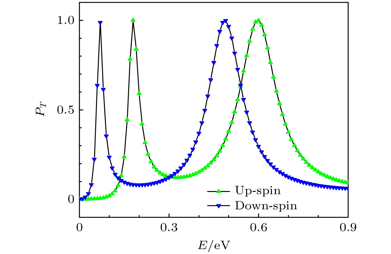
图 2 平面内波矢为 k// = 0.2 nm–1 的自旋向上电子和自旋向下电子隧穿通过 SLSN-InSb 结构(图1)的透射系数, 其他参数为 V = 0.32 eV, d = 8 nm, η = 0.012 eV·nm
Fig. 2. Transmission coefficient for spin-up and spin-down electrons with in-plane wave vector k// = 0.2 nm–1 tunneling through the SLSN-InSb (Fig. 1), where other parameters are V = 0.32 eV, d = 8 nm, η = 0.012 eV·nm.

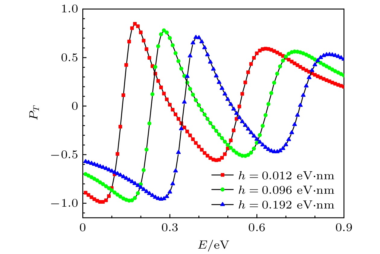
图 4 Rashba型SOC强度不同时, 外加电场对电子自旋极化的影响, 图中其他参数为k// = 0.2 nm–1, V = 0.32 eV, d = 8.0 nm
Fig. 4. Effects of externally applied electric field on the electron-spin polarization for the different Rashba-SOC strengths, where other parameters are k// = 0.2 nm–1, V = 0.32 eV, d = 8.0 nm.

图 5 InSb层厚度不同时, 外加电场对电子自旋极化的影响, 图中其他参数为 k// = 0.2 nm–1, V = 0.32 eV, η = 0.012 eV·nm
Fig. 5. Effects of externally applied electric field on the electron-spin polarization for the different InSb-layer thickness, where other parameters are k// = 0.2 nm–1, V = 0.32 eV, η = 0.012 eV·nm.
-
[1] Faucher J, Sun Y, Jung D, Martin D, Masuda T, Lee M L 2016 Appl. Phys. Lett. 109 172105
Google Scholar
[2] Zhao Y, Xue J S, Zhang J C, Hao Y 2014 Appl. Phys. Lett. 105 223511
Google Scholar
[3] Kang K, Lee K H, Han YM, Gao H, Xie S E, Muller D A, Park J 2017 Nature 550 229
Google Scholar
[4] Soumyanrayanan A, Reyren N, Fert A, Panagopoulos C 2016 Nature 539 509
Google Scholar
[5] Rashba E I, Efros A L 2003 Phys. Rev. Lett. 91 126405
Google Scholar
[6] Miller J B, Zumbuhl D M, Marcus C M, Lyanda-Geller Y B, Goldhaber-Gordon D, Campman K, Gossard A C 2003 Phys. Rev. Lett. 90 076807
Google Scholar
[7] Schliemann J, Loss D 2003 Phys. Rev. B 68 165311
Google Scholar
[8] Kato Y, Myers R C, Gossard A C, Awschalom D D 2004 Nature 427 50
Google Scholar
[9] Žutíc I, Fabiam J, Sarma S D 2004 Rev. Mod. Phys. 76 323
Google Scholar
[10] He Q L, Hughes T L, Armitage N P, Tokura Y, Wang K L 2022 Nature Mater. 21 15
Google Scholar
[11] Koga T, Nitta J, Datta S, Takayanagi H 2002 Phys. Rev. Lett. 88 126601
Google Scholar
[12] Voskoboynikov A, Lin S S, Lee C P 1998 Phys. Rev. B 58 15397
Google Scholar
[13] Voskoboynikov A, Lin S S, Lee C P, Tretyak O 2000 J. Appl. Phys. 87 387
Google Scholar
[14] Perel’ V I, Tarasenko S A, Bel’kov I N, Prettl W 2003 Phys. Rev. B 67 201304
Google Scholar
[15] Tarasenko S A, Perel’ V I, Yassievich I N 2004 Phys. Rev. Lett. 93 056601
Google Scholar
[16] Wang L G, Yang W, Chang K 2005 Phys. Rev. B 72 153314
Google Scholar
[17] Sandu T 2007 Phys. Rev. B 76 197301
Google Scholar
[18] Wang L G, Yang W, Chang K, Chan K S 2007 Phys. Rev. B 76 197302
Google Scholar
[19] Glazov M M, Alekseev P S, Odnoblyudov M A, Chistyakov V M, Tarasenko S A, Yassievich I N 2005 Phys. Rev. B 71 155313
Google Scholar
[20] David Z Y T, Cartoixà X 2002 Appl. Phys. Lett. 81 4198
Google Scholar
[21] Radovanović J, Isić G, Milanović V 2008 Opt. Mater. 30 1134
Google Scholar
[22] Scheid M, Kohda M, Kunihashi Y, Richter K, Nitta J 2008 Phys. Rev. Lett. 101 266401
Google Scholar
[23] Li M, Zhao Z B, Fan L B 2015 Phys. Scripta 90 015806
Google Scholar
[24] Voskoboynikov A, Lin S S, Lee C P 1999 Phys. Rev. B 59 12514
Google Scholar
[25] Erasmo A, Andrada E S, Rocca G C L 1999 Phys. Rev. B 59 15583(R
[26] Ganichev S D, Ivchenko E L, Bel’kov V V, Tarasenko S A, Sollinger M, Weiss D, Wegscheider W, Prettl W 2002 Nature 417 153
Google Scholar
[27] Cao Z L, Lu M W, Huang X H, Guo Q M, Yang S Q 2020 Superlattice Microst. 143 106545
Google Scholar
[28] Cao Z L, Lu M W, Huang X H, Guo Q M, Yang S Q 2020 J. Magn. Magn. Mater. 513 167217
Google Scholar
[29] Cao Z L, Lu M W, Huang X H, Guo Q M, Yang S Q 2021 J. Magn. Magn. Mater. 527 167785
Google Scholar
[30] Cao Z L, Lu M W, Huang X H, Guo Q M, Yang S Q 2021 Physics E 129 114646
Google Scholar
[31] Lu K Y, Lu M W, Chen S Y, Cao X L, Huang X H 2019 J. Magn. Magn. Mater. 491 165491
Google Scholar
[32] Lu M W, Chen S Y, Cao X L, Huang X H 2021 IEEE T. Electron Dev. 68 860
Google Scholar
[33] Gnanasekar K, Navaneethakrishnan K 2005 Physica E 28 328
Google Scholar
[34] Trushin M, Schliemann J 2007 New J. Phys. 9 346
Google Scholar
[35] Safranski C, Sun J Z, Xu J W, Kent A D, Schmidt G, Molenkamp L W 2020 Phys. Rev. Lett. 124 197204
Google Scholar


 下载:
下载:


计量
- 文章访问数: 5610
- PDF下载量: 88
- 被引次数: 0
