-
Relaxor ferroelectric single crystal piezoelectric materials have become the core components of new piezoelectric devices such as ultrasonic transducers used in high-end medical ultrasound diagnostic and therapeutic equipment. High-element density array technology and micro-electro-mechanical systems have developed rapidly. For the new generation of 20–80 MHz medical high-frequency ultrasound transducers, the thickness of high-frequency piezoelectric composite material is usually 20–60 μm, and the width of each piezoelectric column is about 5–15 μm. However, the kerf of traditional cutting-and-filling method is too wide, and it is difficult to reduce the size of the array element, which is not conducive to the density of the array element and the demand for higher frequency applications with higher resolution. In this work, a micromechanical fabrication method based on deep reactive ion etching is used to reduce the slit width and increase the array density. We study the fabrication technology of novel and high-performance relaxor ferroelectric single crystal Mn doped Pb(In1/2Nb1/2)O3-Pb(Mg1/3Nb2/3)O3-PbTiO3 (Mn-PIMNT) micro scale piezoelectric array. The influence of the parameters of lithography and deep reactive ion etching on the morphology of piezoelectric array are studied. We obtain the formation mechanisms of different kerfs, different shapes of piezoelectric array element and the relationship among etching rate of Mn-PIMNT single crystal with antenna power, bias power and etching gas ratio. Finally, the size of piezoelectric array element is less than 10 μm, the etching depth is more than 20 μm, the kerf width is less than 5 μm, the angle is controllable, and the maximum is more than 87°. The ferroelectric domain structure and the regulation of electric field effect of micro scale piezoelectric elements are studied by means of piezoelectric force microscope. The variation rules of piezoelectric properties and micro scale are obtained. This method can effectively bypass the shortcomings of the wide kerf and the destruction of the crystal orientation by the traditional cutting-and-filling method. It provides a new preparation technology for the development of high-frequency piezoelectric composites, high-density ultrasonic transducer arrays and new piezoelectric micro mechanical systems. This project presents the guidance and reference for the new micromachining technology of ferroelectric materials, and also lays the foundation for the high-frequency piezoelectric composite and high-frequency ultrasonic transducer.
[1] Wang D W, Cao M S, Zhang S J 2012 J. Am. Ceram. Soc. 95 3220
 Google Scholar
[2] Wang D W, Cao M S, Zhang S J 2012 Phys. Status Solidi RRL 6 135
 Google Scholar
[3] Wang D W, Cao M S, Zhao Q L, Cui Y, Zhang S J 2013 Phys. Status Solidi RRL 7 221
 Google Scholar
[4] Lee J S, Park E C, Lee S H, Lee D S 2005 Mater. Chem. Phys. 90 381
 Google Scholar
[5] 罗豪甦, 沈关顺, 齐振一, 许桂生, 王评初, 乐秀宏, 李金龙, 仲维卓, 殷之文 1997 人工晶体学报 26 191
Luo H S, Shen G S, Qi Z Y, Xu G S, Wang P C, Le X H, Li J L, Zhong W Z, Yin Z W 1997 J. Synthetic Crystals 26 191
[6] Luo H S, Xu G S, Wang P C, Yin Z W 1999 Ferroelectrics 231 97
 Google Scholar
[7] Xu G S, Luo H S, Xu H Q, Qi Z Y, Wang P C, Zhong W Z, Yin Z W 2001 J. Cryst. Growth. 222 202
 Google Scholar
[8] Feng Z Y, He T H, Xu H Q, Luo H S, Yin Z W 2004 Solid. State. Commun. 130 557
 Google Scholar
[9] Wu X, Liu L H, Li X B, Zhang Q H, Ren B, Lin D, Zhao X Y, Luo H S, Huang Y L 2011 J. Cryst. Growth. 318 865
 Google Scholar
[10] Deng C G, He C J, Chen Z Y, Chen H B, Mao R, Liu Y W, Zhu K J, Gao H F, Ding Y 2019 J. Appl. Phys. 126 085702
 Google Scholar
[11] He C J, Chen Z Y, Chen H B, Wu T, Wang J M, Gu X R, Liu Y W, Zhu K J 2018 J. Nanophotonics 12 046019
 Google Scholar
[12] He C J, Chen H B, Bai F, Fan Z B, Sun L, Xu F, Wang J M, Liu Y W, Zhu K J 2012 J. Appl. Phys. 112 126102
 Google Scholar
[13] Jia Y M, Luo H S, Zhao X Y, Wang F F 2008 Adv. Mater. 20 4776
 Google Scholar
[14] He C J, Chen H B, Wang J M, Gu X R, Wu T, Liu Y W 2015 J. Appl. Phys. 117 164104
 Google Scholar
[15] Yang Y, Jung J H, Yun B K, Zhang F, Pradel K C, Guo W, Wang Z L 2012 Adv. Mater. 24 5357
 Google Scholar
[16] 岳晴雯 2016 博士学位论文 (上海: 中国科学院大学)
Yue Q W 2016 Ph. D. Dissertation (Shanghai: University of Chinese Academy of Sciences) (in Chinese)
[17] Sun E W, Cao W W 2014 Prog. Mater. Sci. 65 124
 Google Scholar
[18] Zhu R F, Zhao J, Liu F, Zhang Z, Fang B J, Chen J W, Xu H Q, Wang X A, Luo H S 2020 J. Am. Ceram. Soc. 103 2575
 Google Scholar
[19] Xie Q X, Hu Y Q, Xue S D, Ma J P, Zhao X Y, Tang Y X, Wang F F, Chew K H, Lin D, Luo H S 2019 Mater. Chem. Phys. 238 121890
 Google Scholar
[20] Zhang J S, Ren W, Jing X P, Shi P, Wu X Q 2015 Ceram. Int. 41 S656
 Google Scholar
[21] Jian X H, Li S B, Huang W B, Cui Y Y, Jiang X N 2015 J. Intell. Mater. Syst. Struct. 26 2011
 Google Scholar
[22] 周丹, 罗来慧, 王飞飞, 贾艳敏, 赵祥永, 罗豪甦 2008 57 4552
 Google Scholar
Zhou D, Luo L H, Wang F F, Jia Y M, Zhao X Y, Luo H S 2008 Acta Phys. Sin. 57 4552
 Google Scholar
[23] 乔学光, 邵志华, 包维佳, 荣强周 2017 66 074205
 Google Scholar
Qiao X G, Shao Z H, Bao W J, Rong Q Z 2017 Acta Phys. Sin. 66 074205
 Google Scholar
[24] 徐萌, 晏建民, 徐志学, 郭磊, 郑仁奎, 李晓光 2018 67 157506
 Google Scholar
Xu M, Yan J M, Xu Z X, Guo L, Zheng R K, Li X G 2018 Acta Phys. Sin. 67 157506
 Google Scholar
[25] 赵章风, 张文俊, 牛丽丽, 孟龙, 郑海荣 2018 67 194302
 Google Scholar
Zhao Z F, Zhang W J, Niu L L, Meng L, Zheng H R 2018 Acta Phys. Sin. 67 194302
 Google Scholar
[26] Wang J S, Xiao J J, Zhao X Y, Wang F F, Tang Y X, Zhang Q Z, Fang B J, Zhu R F, Yue Q W, Liu D X, Deng J 2020 Ceram. Int. 46 11913
 Google Scholar
[27] Nakano N, Petrovic Z L, Makabe T 1994 Jpn. J. Appl. Phys. 33 2223
 Google Scholar
[28] Crintea D L, Czarnetzki U, Iordanova S, Koleva I, Luggenholscher D 2009 J. Phys. D: Appl. Phys. 42 045208
 Google Scholar
[29] Sakoda T, Okraku-Yirenkyi Y, Youl-Moon S, Otsubo M, Chikahisa H 2001 Jpn. J. Appl. Phys. 40 6607
 Google Scholar
[30] Uchida T, Hamaguchi S 2008 J. Phys. D: Appl. Phys. 41 083001
 Google Scholar
[31] Wang Y J, Luo C T, Wang S H, Chen C, Yuan G L, Luo H S, Viehland D 2020 Adv. Electron. Mater. 6 1900949
 Google Scholar
[32] Li Y, Lu G X, Chen J J, Jing J C, Huo T C, Chen R M, Jiang L M, Zhou Q F, Chen Z P 2019 Photoacoustics 15 100138
 Google Scholar
[33] Jiang L M, Chen R M, Xing J, Lu G X, Li R Z, Jiang Y, Shung K K, Zhu J G, Zhou Q F 2019 J. Appl. Phys. 125 214501
 Google Scholar
[34] Zhou Q F, Lam K H, Zheng H R, Qiu W B, Shung K K 2014 Prog. Mater. Sci. 66 87
 Google Scholar
[35] Zhang J S, Ren W, Liu Y T, Wu X Q, Fei C L, Quan Y, Zhou Q F 2018 Sensors 18 1
 Google Scholar
-
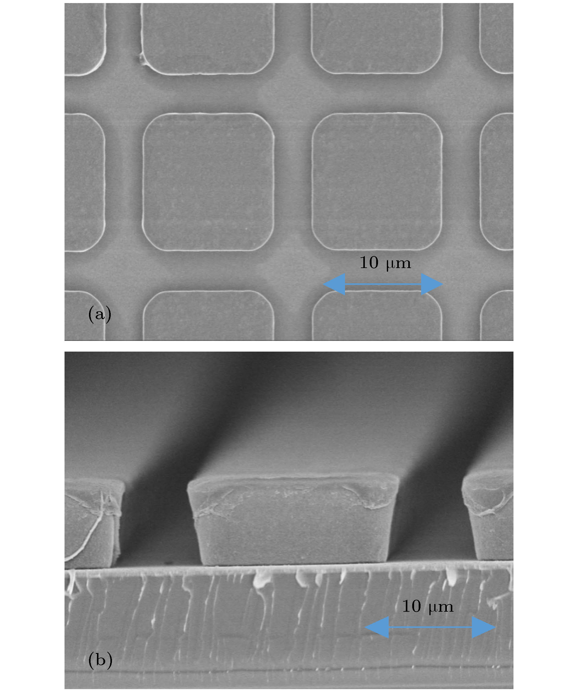
图 2 紫外光刻实验结果 (a), (b) 阵元尺寸为12.94 μm时, 光学显微镜下的表面形貌和扫描电子显微镜下的截面图; (c), (d) 阵元尺寸为13.97 μm时, 光学显微镜下的表面形貌和扫描电子显微镜下的截面图
Figure 2. Results of lithography: (a), (b) Surface morphology under optical microscope and cross section under scanning electron microscope when the element size is 12.94 μm; (c), (d) surface morphology under optical microscope and cross section under scanning electron microscope when the element size is 13.97 μm.
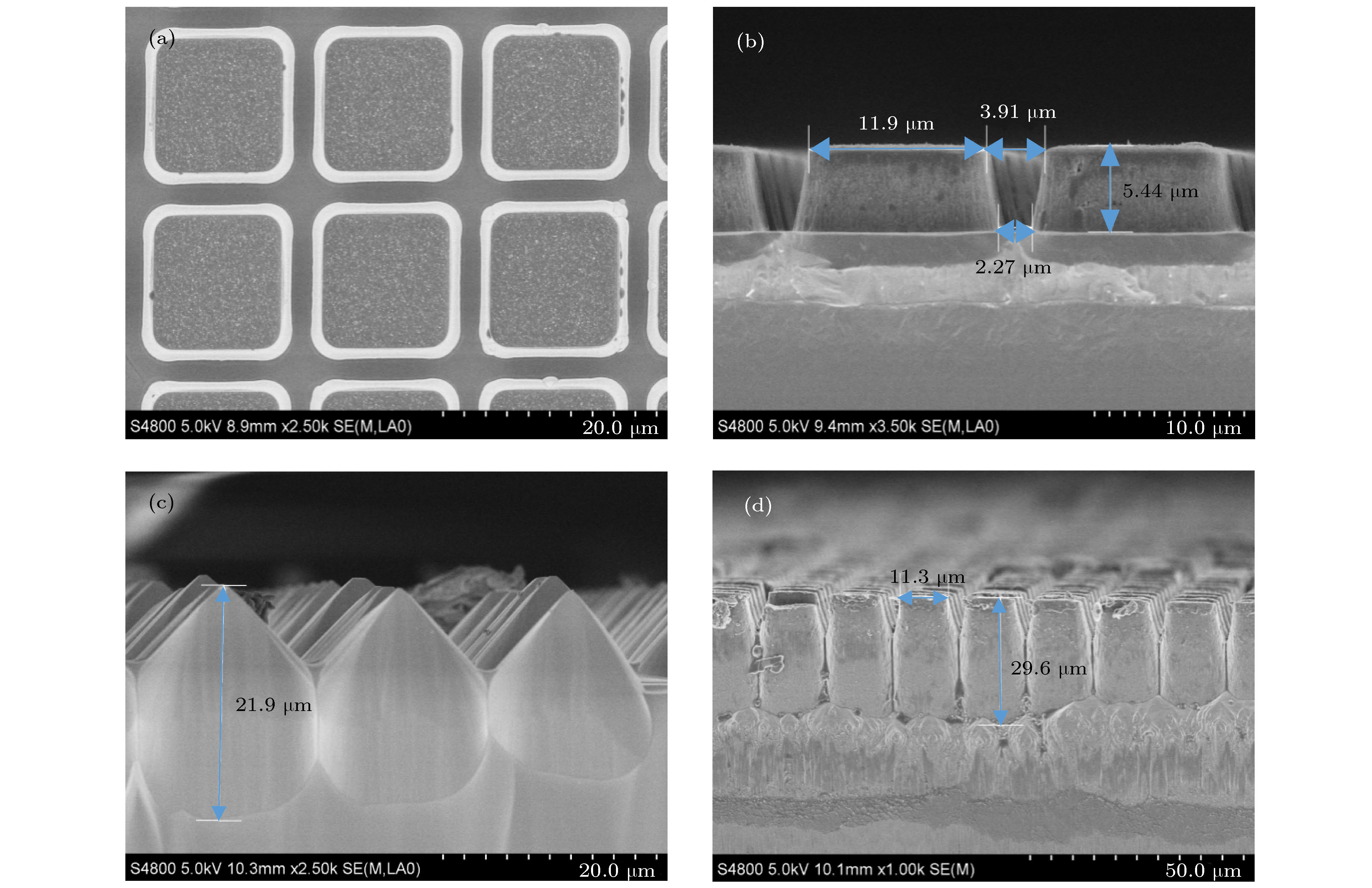
图 6 刻蚀结果 (a) 高密度面阵表面形貌; (b) 高密度面阵截面形貌; (c) 锥形阵列截面形貌; (d) 深刻蚀高密度面阵截面形貌
Figure 6. Etching results: (a) Surface morphology of high density array; (b) cross section morphology of high density array; (c) cross section morphology of conical array; (d) the surface morphology of deep etching of high density surface array.
图 7 压电力显微镜下的不同尺度区域结构 (a) 30 μm × 30 μm区域的表面形貌; (b) 30 μm × 30 μm区域的面外振幅; (c) 30 μm × 30 μm区域的相位; (d) 5 μm × 5 μm区域的表面形貌; (e) 5 μm × 5 μm区域的面外振幅; (f) 5 μm × 5 μm区域的相位; (g) 1 μm × 1 μm区域的表面形貌; (h) 1 μm × 1 μm区域的面外振幅; (i) 1 μm × 1 μm区域的相位
Figure 7. Structure of different scale areas under the piezoelectric microscope: (a) Surface morphology of 30 μm × 30 μm area; (b) out of plane amplitude of 30 μm × 30 μm area; (c) phase of 30 μm × 30 μm area; (d) surface morphology of 5 μm × 5 μm area; (e) out of plane amplitude of 5 μm × 5 μm area; (f) phase of 5 μm × 5 μm area; (g) surface morphology of 1 μm × 1 μm area; (h) out of plane amplitude of 1 μm × 1 μm area; (i) phase of 1 μm × 1 μm area.
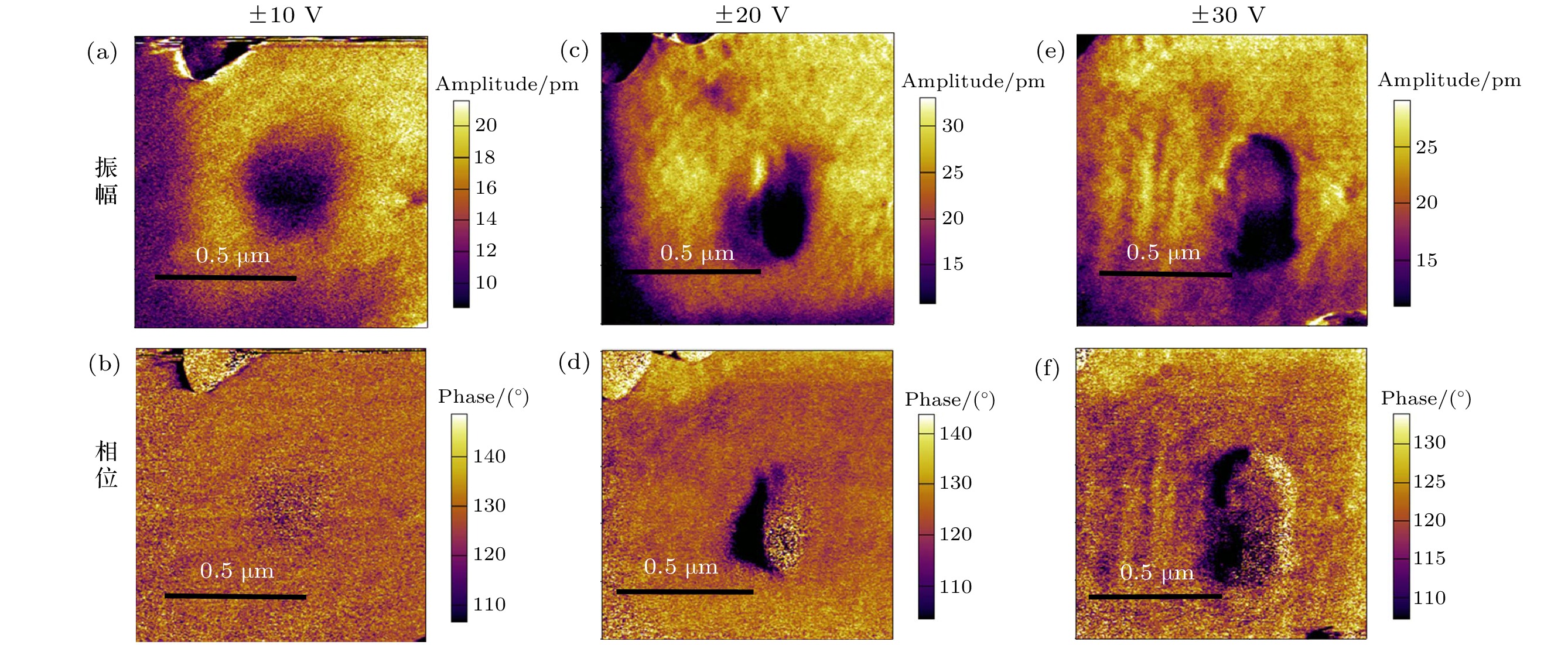
图 8 压电力显微镜下1 μm × 1 μm区域的结果 (a) ± 10 V电压下的面外振幅; (b) ± 10 V电压下的相位; (c) ± 20 V电压下的面外振幅; (d) ± 20 V电压下的相位; (e) ± 30 V电压下的面外振幅; (f) ± 30 V电压下的相位
Figure 8. Results of 1 μm × 1 μm area under the piezoelectric force microscope: (a) Out of plane amplitude at ± 10 V; (b) phase at ± 10 V; (c) out of plane amplitude at ± 20 V; (d) phase at ± 20 V; (e) out of plane amplitude at ± 30 V; (f) phase at ± 30 V.
表 1 电镀液配料成分及含量
Table 1. Composition and content of electroplate bath ingredients.
成分 含量 氨基磺酸镍/g·L–1 280—400 硼酸/g·L–1 40—50 阳极活化剂/g·L–1 60—100 润湿剂/mL·L–1 1—5 去应力剂 适量 -
[1] Wang D W, Cao M S, Zhang S J 2012 J. Am. Ceram. Soc. 95 3220
 Google Scholar
[2] Wang D W, Cao M S, Zhang S J 2012 Phys. Status Solidi RRL 6 135
 Google Scholar
[3] Wang D W, Cao M S, Zhao Q L, Cui Y, Zhang S J 2013 Phys. Status Solidi RRL 7 221
 Google Scholar
[4] Lee J S, Park E C, Lee S H, Lee D S 2005 Mater. Chem. Phys. 90 381
 Google Scholar
[5] 罗豪甦, 沈关顺, 齐振一, 许桂生, 王评初, 乐秀宏, 李金龙, 仲维卓, 殷之文 1997 人工晶体学报 26 191
Luo H S, Shen G S, Qi Z Y, Xu G S, Wang P C, Le X H, Li J L, Zhong W Z, Yin Z W 1997 J. Synthetic Crystals 26 191
[6] Luo H S, Xu G S, Wang P C, Yin Z W 1999 Ferroelectrics 231 97
 Google Scholar
[7] Xu G S, Luo H S, Xu H Q, Qi Z Y, Wang P C, Zhong W Z, Yin Z W 2001 J. Cryst. Growth. 222 202
 Google Scholar
[8] Feng Z Y, He T H, Xu H Q, Luo H S, Yin Z W 2004 Solid. State. Commun. 130 557
 Google Scholar
[9] Wu X, Liu L H, Li X B, Zhang Q H, Ren B, Lin D, Zhao X Y, Luo H S, Huang Y L 2011 J. Cryst. Growth. 318 865
 Google Scholar
[10] Deng C G, He C J, Chen Z Y, Chen H B, Mao R, Liu Y W, Zhu K J, Gao H F, Ding Y 2019 J. Appl. Phys. 126 085702
 Google Scholar
[11] He C J, Chen Z Y, Chen H B, Wu T, Wang J M, Gu X R, Liu Y W, Zhu K J 2018 J. Nanophotonics 12 046019
 Google Scholar
[12] He C J, Chen H B, Bai F, Fan Z B, Sun L, Xu F, Wang J M, Liu Y W, Zhu K J 2012 J. Appl. Phys. 112 126102
 Google Scholar
[13] Jia Y M, Luo H S, Zhao X Y, Wang F F 2008 Adv. Mater. 20 4776
 Google Scholar
[14] He C J, Chen H B, Wang J M, Gu X R, Wu T, Liu Y W 2015 J. Appl. Phys. 117 164104
 Google Scholar
[15] Yang Y, Jung J H, Yun B K, Zhang F, Pradel K C, Guo W, Wang Z L 2012 Adv. Mater. 24 5357
 Google Scholar
[16] 岳晴雯 2016 博士学位论文 (上海: 中国科学院大学)
Yue Q W 2016 Ph. D. Dissertation (Shanghai: University of Chinese Academy of Sciences) (in Chinese)
[17] Sun E W, Cao W W 2014 Prog. Mater. Sci. 65 124
 Google Scholar
[18] Zhu R F, Zhao J, Liu F, Zhang Z, Fang B J, Chen J W, Xu H Q, Wang X A, Luo H S 2020 J. Am. Ceram. Soc. 103 2575
 Google Scholar
[19] Xie Q X, Hu Y Q, Xue S D, Ma J P, Zhao X Y, Tang Y X, Wang F F, Chew K H, Lin D, Luo H S 2019 Mater. Chem. Phys. 238 121890
 Google Scholar
[20] Zhang J S, Ren W, Jing X P, Shi P, Wu X Q 2015 Ceram. Int. 41 S656
 Google Scholar
[21] Jian X H, Li S B, Huang W B, Cui Y Y, Jiang X N 2015 J. Intell. Mater. Syst. Struct. 26 2011
 Google Scholar
[22] 周丹, 罗来慧, 王飞飞, 贾艳敏, 赵祥永, 罗豪甦 2008 57 4552
 Google Scholar
Zhou D, Luo L H, Wang F F, Jia Y M, Zhao X Y, Luo H S 2008 Acta Phys. Sin. 57 4552
 Google Scholar
[23] 乔学光, 邵志华, 包维佳, 荣强周 2017 66 074205
 Google Scholar
Qiao X G, Shao Z H, Bao W J, Rong Q Z 2017 Acta Phys. Sin. 66 074205
 Google Scholar
[24] 徐萌, 晏建民, 徐志学, 郭磊, 郑仁奎, 李晓光 2018 67 157506
 Google Scholar
Xu M, Yan J M, Xu Z X, Guo L, Zheng R K, Li X G 2018 Acta Phys. Sin. 67 157506
 Google Scholar
[25] 赵章风, 张文俊, 牛丽丽, 孟龙, 郑海荣 2018 67 194302
 Google Scholar
Zhao Z F, Zhang W J, Niu L L, Meng L, Zheng H R 2018 Acta Phys. Sin. 67 194302
 Google Scholar
[26] Wang J S, Xiao J J, Zhao X Y, Wang F F, Tang Y X, Zhang Q Z, Fang B J, Zhu R F, Yue Q W, Liu D X, Deng J 2020 Ceram. Int. 46 11913
 Google Scholar
[27] Nakano N, Petrovic Z L, Makabe T 1994 Jpn. J. Appl. Phys. 33 2223
 Google Scholar
[28] Crintea D L, Czarnetzki U, Iordanova S, Koleva I, Luggenholscher D 2009 J. Phys. D: Appl. Phys. 42 045208
 Google Scholar
[29] Sakoda T, Okraku-Yirenkyi Y, Youl-Moon S, Otsubo M, Chikahisa H 2001 Jpn. J. Appl. Phys. 40 6607
 Google Scholar
[30] Uchida T, Hamaguchi S 2008 J. Phys. D: Appl. Phys. 41 083001
 Google Scholar
[31] Wang Y J, Luo C T, Wang S H, Chen C, Yuan G L, Luo H S, Viehland D 2020 Adv. Electron. Mater. 6 1900949
 Google Scholar
[32] Li Y, Lu G X, Chen J J, Jing J C, Huo T C, Chen R M, Jiang L M, Zhou Q F, Chen Z P 2019 Photoacoustics 15 100138
 Google Scholar
[33] Jiang L M, Chen R M, Xing J, Lu G X, Li R Z, Jiang Y, Shung K K, Zhu J G, Zhou Q F 2019 J. Appl. Phys. 125 214501
 Google Scholar
[34] Zhou Q F, Lam K H, Zheng H R, Qiu W B, Shung K K 2014 Prog. Mater. Sci. 66 87
 Google Scholar
[35] Zhang J S, Ren W, Liu Y T, Wu X Q, Fei C L, Quan Y, Zhou Q F 2018 Sensors 18 1
 Google Scholar
Catalog
Metrics
- Abstract views: 8425
- PDF Downloads: 117
- Cited By: 0


 DownLoad:

