-
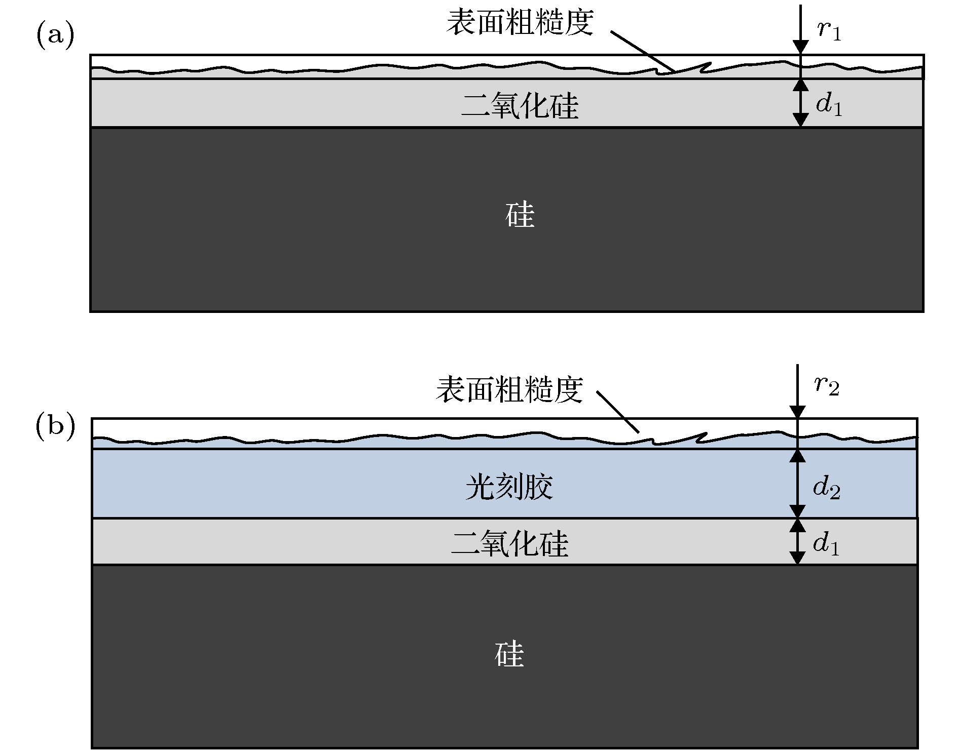
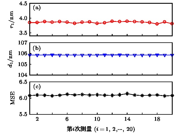
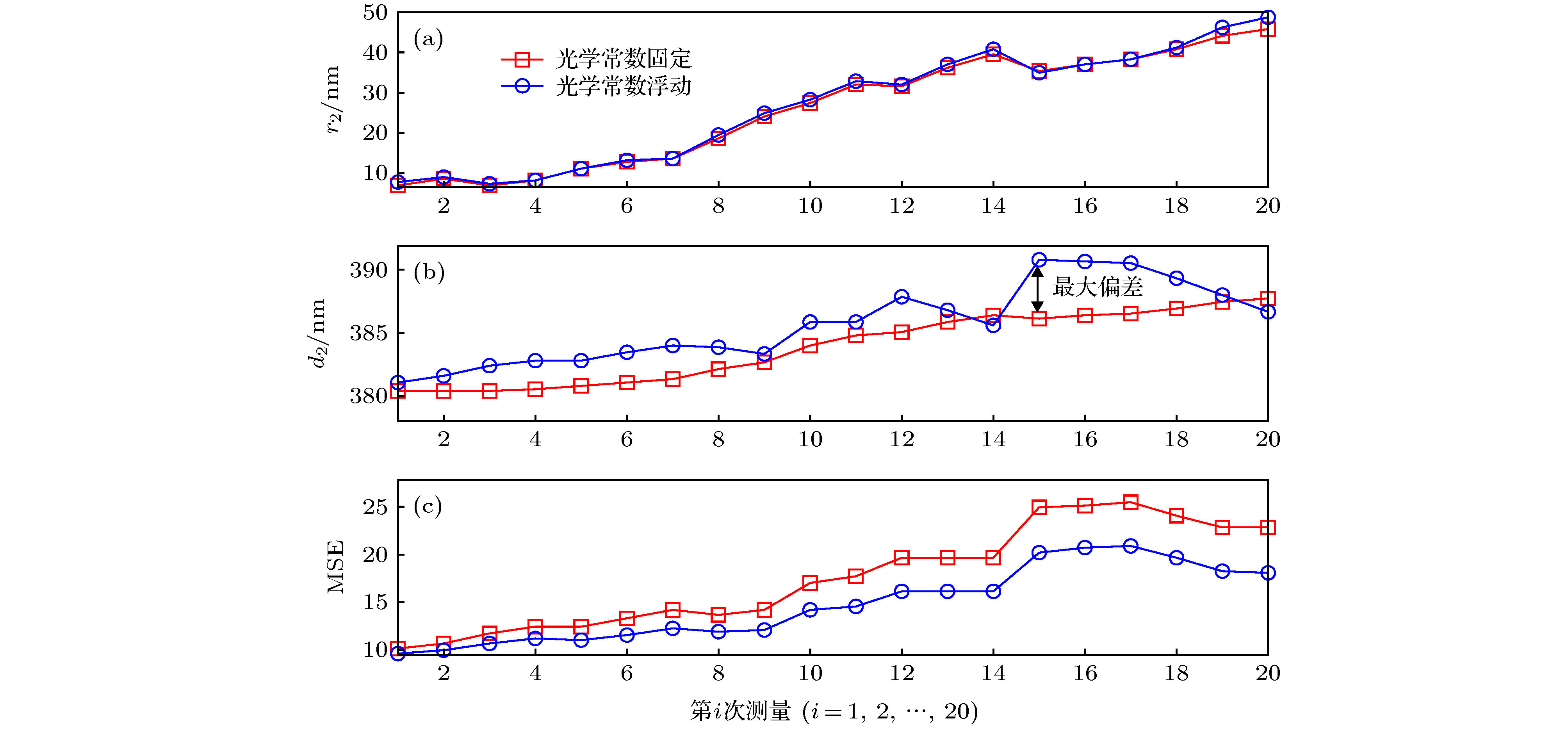
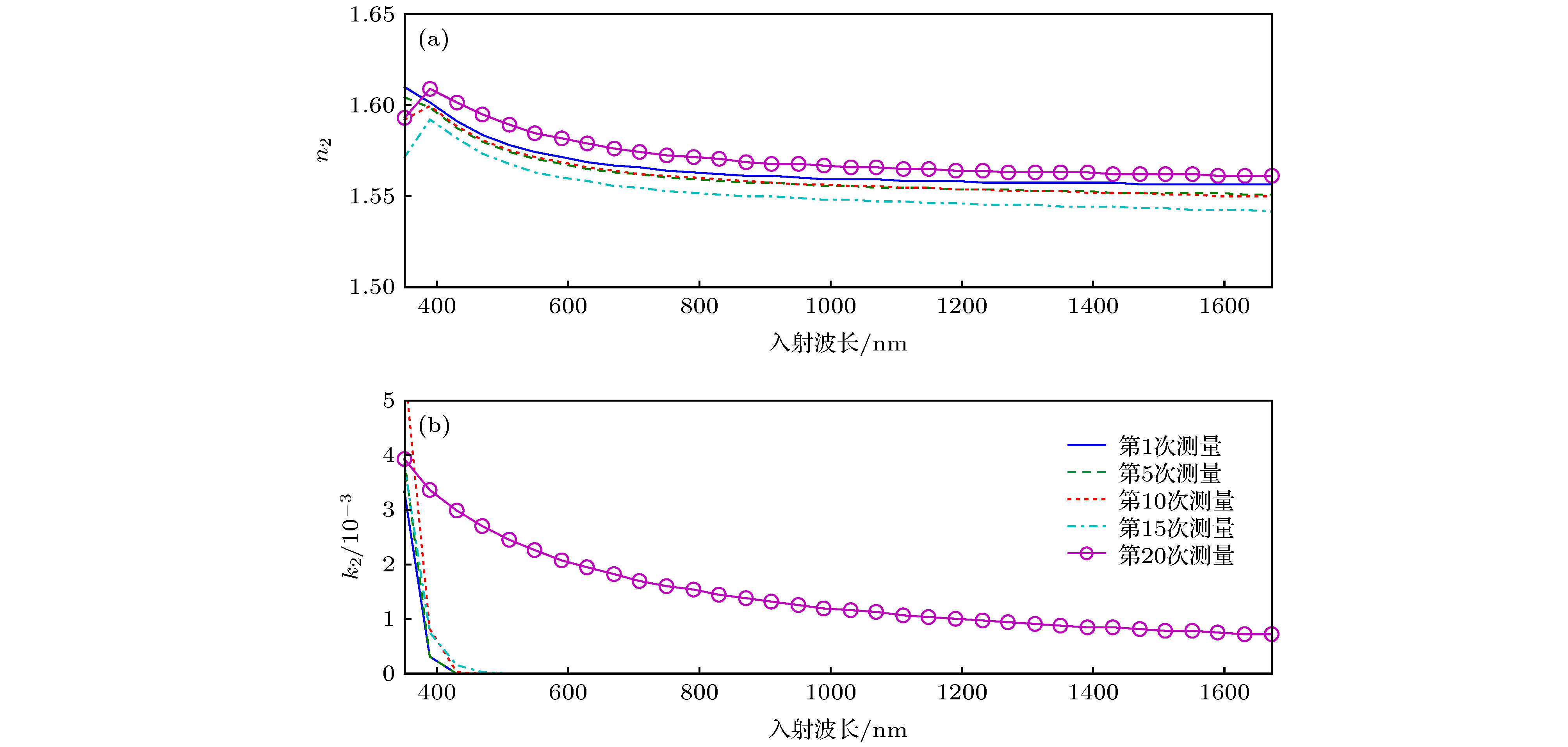
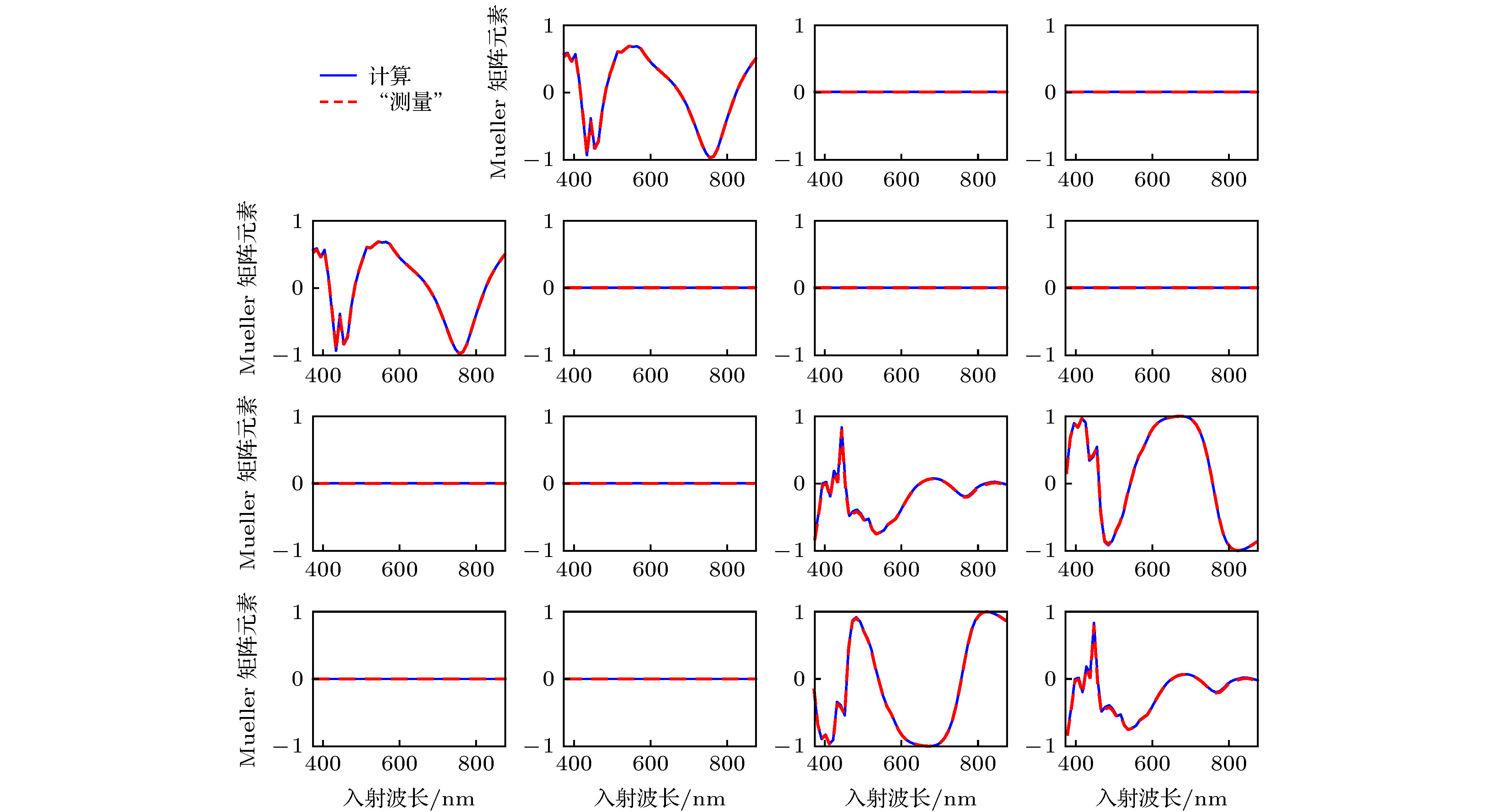
Optical scatterometry, as a fast, low-cost, and non-contact measurement instrument, is widely used in the profile characterization of nanostructure in the semiconductor manufacturing industry. In general, it involves two procedures, i.e. the forward optical modeling of sub-wavelength nanostructures and the reconstruction of structural profiles from the measured signatures. Here, the general term signature means the scattered light information from the diffractive grating structure, which can be in the form of reflectance, ellipsometric angles, Stokes vector elements, or Mueller matrix elements. The profile reconstruction process is an inverse problem with the objective of optimizing a set of floating profile parameters (e.g., critical dimension, sidewall angle, and height) whose theoretical signatures can best match the measured ones through regression analysis or library search. During solving the inverse problem, the refractive index and distinction coefficient of the material of nanostructure are assumed to be constants and they are generally fixed. This assumption is valid for most of the materials in semiconductor industry, but not for certain materials that are very photosensitive. That is, the optical constants of photosensitive materials may vary with the illumination time of the incident light beam in spectroscopic ellipsometer, and the error caused by the variation of optical constants propagates to the final extracted results of structural profiles, which should not be neglected, especially for high precision and accuracy metrology. Experiments performed on SiO2 and polymethyl methacrylate (PMMA) thin films are conducted and demonstrate that the extracted geometric parameters and optical constants of SiO2 film do not change with illumination time increasing, while the twenty groups of values of extracted refractive index n and distinction coefficient k of PMMA resist film vary obviously, and the difference between the extracted maximum and minimum film thickness has reached 40.5 nm, which to some extent illustrates that the above assumption is not valid for PMMA resist, so that the incident light beam of spectroscopic ellipsometer has a great influence on the extracted film thickness. Further, simulations based on a three-dimensional PMMA grating also indicate that the error of optical constant has considerably transferred to the extracted profile parameters. This finding is of significance for improving the accuracy of nanostructure characterization in optical scatterometry. -
Keywords:
- optical scatterometry /
- photoresist nanostructure /
- polymethyl methacrylate /
- optical constant
[1] Fang F Z, Zhang X D, Gao W, Guo Y B, Byrne G, Hansen H N 2017 CIRP Ann.- Manuf. Technol. 66 683
 Google Scholar
[2] 刘宇宏, 雒建斌 2013 中国基础科学 15 3
 Google Scholar
Liu Y H, Luo J B 2013 China Basic Sci. 15 3
 Google Scholar
[3] Fujiwara H 2007 Spectroscopic Ellipsometry Principles and Applications (New York: John Wiley & Sons Inc) pp81–141
[4] Liu J M, Lin J B, Jiang H, Gu H G, Chen X G, Zhang C W, Liao G L, Liu S Y 2019 Phys. Scripta 94 085802
 Google Scholar
[5] Sunkoju S, Schujman S, Dixit D, Diebold A, Li J, Collins R, Haldar P 2016 Thin Solid Films 606 113
 Google Scholar
[6] Matthias W, Johannes E, Jürgen P, Max S, Alexander D, Bernd B 2017 Opt. Express 25 2460
 Google Scholar
[7] 陈修国, 刘世元, 张传维, 吴懿平, 马智超, 孙堂友, 徐智谋 2014 63 180701
 Google Scholar
Chen X G, Liu S Y, Zhang C W, Wu Y P, Ma Z C, Sun T Y, Xu Z M 2014 Acta Phys. Sin. 63 180701
 Google Scholar
[8] Huang H T, Kong W, Terry Jr F L 2001 Appl. Phys. Lett. 78 3983
 Google Scholar
[9] 张铮, 徐智谋, 孙堂友, 何健, 徐海峰, 张学明, 刘世元 2013 62 168102
 Google Scholar
Zhang Z, Xu Z M, Sun T Y, He J, Xu H F, Zhang X M, Liu S Y 2013 Acta Phys.Sin 62 168102
 Google Scholar
[10] Chen X, Zhang C, and Liu S 2013 Appl. Phys. Lett. 103 151605
 Google Scholar
[11] Liu S, Chen X, and Zhang C 2015 Thin Solid Films 584 176
 Google Scholar
[12] Moharam M G, Grann E B, Pommet D A 1995 J. Opt. Soc. Am. A 12 1068
 Google Scholar
[13] Zhu J L, Liu S Y, Zhang C W, Chen X G, Dong Z Q 2013 J. Micro-Nanolith. Mem. 12 013004
[14] Ichikawa H 1998 J. Opt. Soc. Am. A 15 152
[15] Nakata Y, Koshiba M 1990 J. Opt. Soc. Am. A 7 1494
 Google Scholar
[16] 傅克祥, 王植恒, 张大跃, 张靖, 张奇志 1999 中国科学(A辑) 29 356
Fu K X, Wang Z H, Zhang D Y, Zhang J, Zhang Q Z 1999 Sci. China Ser. A 29 356
[17] Moharam M G, Pommet D A, Grann E B, Gaylord T K 1995 J. Opt. Soc. Am. A 12 1077
 Google Scholar
[18] Raymond C J, Littau M E, Chuprin A, Ward S 2004 Proceedings of SPIE Santa Clara, California, United States, May 24, 2004 p564
[19] Levenberg, K 1944 Quart. Appl. Math. 2 164
 Google Scholar
[20] Hanke, M 1997 Inverse Probl. 13 79
 Google Scholar
[21] Vagos P, Hu J, Liu Z, Rabello S 2009 Proc. SPIE 7272 72721N
 Google Scholar
[22] Littau M, Forman D, Bruce J, Raymond C J, Hummel S G 2006 Proceedings of SPIE San Jose, California, United States, March 24, 2006 p615236
[23] Chen X, Liu S, Zhang C, Jiang H, Ma Z, Sun T, Xu Z 2014 Opt. Express 22 15165
 Google Scholar
[24] Chen X, Liu S, Zhang C, Jiang H 2013 J. Micro-Nanolith. Mem. 12 033013
[25] Dong Z, Liu S, Chen X, Zhang C 2014 Thin Solid Films 562 16
 Google Scholar
[26] Li Y G, Susumu S 2007 Microsyst. Technol. 13 227
[27] 李以贵, 颜平, 黄远, 杉山进 2016 红外与激光工程 45 0620001
Li Y G, Yan P, Huang Y, Susumu S 2016 Infrared Laser Eng. 45 0620001
[28] Li L 1996 J. Opt. Soc. Am. A 13 1870
 Google Scholar
[29] Marquardt D 1963 J. Soc. Indust. Appl. Math. 11 431
[30] Collins R W, Koh J 1999 J.Opt. Soc. Am. A 16 1997
 Google Scholar
[31] Shekar P V, Latha D M, Pisipati V G K M 2017 Opt. Mater. 64 564
 Google Scholar
[32] Zhang Y H, Zhou X Q, Cao K, Chen X G, Deng Z, Liu S Y, Shan B, Chen R 2015 Thin Solid Films 593 144
 Google Scholar
[33] Nidamanuri R R, Zbell B 2010 Prog. Phys. Geog. 34 47
 Google Scholar
[34] Herzinger C M, Johs B, McGahan W A, Woollam J A, Paulson M 1998 J. Appl. Phys 83 3323
 Google Scholar
[35] 韩建, 巴音贺希格, 李文昊, 孔鹏 2012 光学精密工程 20 2380
 Google Scholar
Han J, Bayanheshig, Li W H, Kong P 2012 Opt. Precis. Eng. 20 2380
 Google Scholar
-
表 1 对比PMMA仿真光栅3个待测形貌参数的拟合值与真实值
Table 1. Comparison of these three true dimensions and the extracted results of the simulated PMMA grating.
参数名称 真实值 拟合值 绝对误差 顶部线宽w1/nm 350.00 352.90 2.90 线高h/nm 387.42 387.90 0.50 底部线宽w2/nm 365.00 368.50 0.35 -
[1] Fang F Z, Zhang X D, Gao W, Guo Y B, Byrne G, Hansen H N 2017 CIRP Ann.- Manuf. Technol. 66 683
 Google Scholar
[2] 刘宇宏, 雒建斌 2013 中国基础科学 15 3
 Google Scholar
Liu Y H, Luo J B 2013 China Basic Sci. 15 3
 Google Scholar
[3] Fujiwara H 2007 Spectroscopic Ellipsometry Principles and Applications (New York: John Wiley & Sons Inc) pp81–141
[4] Liu J M, Lin J B, Jiang H, Gu H G, Chen X G, Zhang C W, Liao G L, Liu S Y 2019 Phys. Scripta 94 085802
 Google Scholar
[5] Sunkoju S, Schujman S, Dixit D, Diebold A, Li J, Collins R, Haldar P 2016 Thin Solid Films 606 113
 Google Scholar
[6] Matthias W, Johannes E, Jürgen P, Max S, Alexander D, Bernd B 2017 Opt. Express 25 2460
 Google Scholar
[7] 陈修国, 刘世元, 张传维, 吴懿平, 马智超, 孙堂友, 徐智谋 2014 63 180701
 Google Scholar
Chen X G, Liu S Y, Zhang C W, Wu Y P, Ma Z C, Sun T Y, Xu Z M 2014 Acta Phys. Sin. 63 180701
 Google Scholar
[8] Huang H T, Kong W, Terry Jr F L 2001 Appl. Phys. Lett. 78 3983
 Google Scholar
[9] 张铮, 徐智谋, 孙堂友, 何健, 徐海峰, 张学明, 刘世元 2013 62 168102
 Google Scholar
Zhang Z, Xu Z M, Sun T Y, He J, Xu H F, Zhang X M, Liu S Y 2013 Acta Phys.Sin 62 168102
 Google Scholar
[10] Chen X, Zhang C, and Liu S 2013 Appl. Phys. Lett. 103 151605
 Google Scholar
[11] Liu S, Chen X, and Zhang C 2015 Thin Solid Films 584 176
 Google Scholar
[12] Moharam M G, Grann E B, Pommet D A 1995 J. Opt. Soc. Am. A 12 1068
 Google Scholar
[13] Zhu J L, Liu S Y, Zhang C W, Chen X G, Dong Z Q 2013 J. Micro-Nanolith. Mem. 12 013004
[14] Ichikawa H 1998 J. Opt. Soc. Am. A 15 152
[15] Nakata Y, Koshiba M 1990 J. Opt. Soc. Am. A 7 1494
 Google Scholar
[16] 傅克祥, 王植恒, 张大跃, 张靖, 张奇志 1999 中国科学(A辑) 29 356
Fu K X, Wang Z H, Zhang D Y, Zhang J, Zhang Q Z 1999 Sci. China Ser. A 29 356
[17] Moharam M G, Pommet D A, Grann E B, Gaylord T K 1995 J. Opt. Soc. Am. A 12 1077
 Google Scholar
[18] Raymond C J, Littau M E, Chuprin A, Ward S 2004 Proceedings of SPIE Santa Clara, California, United States, May 24, 2004 p564
[19] Levenberg, K 1944 Quart. Appl. Math. 2 164
 Google Scholar
[20] Hanke, M 1997 Inverse Probl. 13 79
 Google Scholar
[21] Vagos P, Hu J, Liu Z, Rabello S 2009 Proc. SPIE 7272 72721N
 Google Scholar
[22] Littau M, Forman D, Bruce J, Raymond C J, Hummel S G 2006 Proceedings of SPIE San Jose, California, United States, March 24, 2006 p615236
[23] Chen X, Liu S, Zhang C, Jiang H, Ma Z, Sun T, Xu Z 2014 Opt. Express 22 15165
 Google Scholar
[24] Chen X, Liu S, Zhang C, Jiang H 2013 J. Micro-Nanolith. Mem. 12 033013
[25] Dong Z, Liu S, Chen X, Zhang C 2014 Thin Solid Films 562 16
 Google Scholar
[26] Li Y G, Susumu S 2007 Microsyst. Technol. 13 227
[27] 李以贵, 颜平, 黄远, 杉山进 2016 红外与激光工程 45 0620001
Li Y G, Yan P, Huang Y, Susumu S 2016 Infrared Laser Eng. 45 0620001
[28] Li L 1996 J. Opt. Soc. Am. A 13 1870
 Google Scholar
[29] Marquardt D 1963 J. Soc. Indust. Appl. Math. 11 431
[30] Collins R W, Koh J 1999 J.Opt. Soc. Am. A 16 1997
 Google Scholar
[31] Shekar P V, Latha D M, Pisipati V G K M 2017 Opt. Mater. 64 564
 Google Scholar
[32] Zhang Y H, Zhou X Q, Cao K, Chen X G, Deng Z, Liu S Y, Shan B, Chen R 2015 Thin Solid Films 593 144
 Google Scholar
[33] Nidamanuri R R, Zbell B 2010 Prog. Phys. Geog. 34 47
 Google Scholar
[34] Herzinger C M, Johs B, McGahan W A, Woollam J A, Paulson M 1998 J. Appl. Phys 83 3323
 Google Scholar
[35] 韩建, 巴音贺希格, 李文昊, 孔鹏 2012 光学精密工程 20 2380
 Google Scholar
Han J, Bayanheshig, Li W H, Kong P 2012 Opt. Precis. Eng. 20 2380
 Google Scholar
Catalog
Metrics
- Abstract views: 13811
- PDF Downloads: 222
- Cited By: 0


 DownLoad:

