-
The manipulation of electronic structures of conventional semiconductors remains the key issue of modern semiconductor physics and devices. Compare to limited modulation of semiconductors by conventional gate technique, we theoretically demonstrate that, polarized interfaces can generate a strong built-in electric field (about 10 MV/cm) in both polar and non-polar semiconductors, and the polarized interfaces can tune the band gaps in a wide range (approximately 0—2 eV), and significantly enhances the Rashba spin-orbit coupling strength as well. In this paper, we introduce polarized interfaces in polar semiconductor InN and non-polar semiconductor Ge, and generate topological insulator phases by polarized interfaces. The polarized interface is compatible with conventional semiconductor fabrication techniques and shows interesting physics and potential optoelectronic applications.
-
Keywords:
- spin-orbit coupling /
- polarization /
- interfaces /
- semiconductors
[1] Klitzing K V, Dorda G, Pepper M 1980 Physical Review Letters 45 494
 Google Scholar
[2] Tsui D C, Stormer H L, Gossard A C 1982 Physical Review Letters 48 1559
 Google Scholar
[3] Haldane F D M 1988 Physical Review Letters 61 2015
 Google Scholar
[4] Chang C Z, Zhang J, Feng X, Shen J, Zhang Z, Guo M, Li K, Ou Y, Wei P, Wang L L, Ji Z Q, Feng Y, Ji S, Chen X, Jia J, Dai X, Fang Z, Zhang S C, He K, Wang Y, Lu L, Ma X C, Xue Q K 2013 Science 340 167
 Google Scholar
[5] Hasan M Z, Kane C L 2010 Rev. Mod. Phys. 82 3045
 Google Scholar
[6] He Q L, Pan L, Stern A L, Burks E C, Che X, Yin G, Wang J, Lian B, Zhou Q, Choi E S, Murata K, Kou X, Chen Z, Nie T, Shao Q, Fan Y, Zhang S C, Liu K, Xia J, Wang K L 2017 Science 357 294
 Google Scholar
[7] Weng H, Fang C, Fang Z, Bernevig B A, Dai X 2015 Physical Review X 5 011029
[8] Yoshida S, Misawa S, Gonda S 1983 Appl. Phys. Lett. 42 427
 Google Scholar
[9] Amano H, Sawaki N, Akasaki I, Toyoda Y 1986 Appl. Phys. Lett. 48 353
 Google Scholar
[10] Asif Khan M, Kuznia J N, Olson D T, George T, Pike W T 1993 Appl. Phys. Lett. 63 3470
 Google Scholar
[11] Hwang H Y, Iwasa Y, Kawasaki M, Keimer B, Nagaosa N, Tokura Y 2012 Nat. Mater. 11 103
 Google Scholar
[12] Natural Editorial 2012 Nat. Mater. 11 91
[13] Seibold G, Caprara S, Grilli M, Raimondi R 2017 Physical Review Letters 119 256801
 Google Scholar
[14] Kroemer H 2001 Rev. Mod. Phys. 73 783
 Google Scholar
[15] Bernardini F, Fiorentini V, Vanderbilt D 1997 Physical Review B 56 R10024
 Google Scholar
[16] Xia J-B 1989 Physical Review B 40 8500
 Google Scholar
[17] 夏建白, 朱邦芬 1995 半导体超晶格物理 (上海: 上海科学技术出版社)
Xia J B, Zhu B F 1995 Semiconductor Superlattice Physics(Shanghai: Shanghai Scientific & Technical Publishers) (in Chinese)
[18] 褚君浩 2005 窄禁带半导体物理学 (1 Ed.) (北京: 科学出版社)
Chu J H 2005 Narrow Gap Semiconductor Physics (1 Ed.) (Beijing: Science Press) (in Chinese)
[19] Miao M S, Yan Q, Van de Walle C G, Lou W K, Li L L, Chang K 2012 Phys. Rev. Lett. 109 186803
 Google Scholar
[20] Bernevig B A, Hughes T L, Zhang S C 2006 Science 314 1757
 Google Scholar
[21] Nitta J, Akazaki T, Takayanagi H, Enoki T 1997 Physical Review Letters 78 1335
 Google Scholar
[22] Grundler D 2000 Phys. Rev. Lett. 84 6074
 Google Scholar
[23] Winkler R 2003 Spin-Orbit Coupling Effects in Two-Dimensional Electron and Hole Systems (Springer)
[24] Zawadzki W, Pfeffer P 2004 Semicond. Sci. Technol. 19 R1
 Google Scholar
[25] Yang W, Chang K, Zhang S C 2008 Phys. Rev. Lett. 100 056602
 Google Scholar
[26] Li J, Chang K 2009 Appl. Phys. Lett. 95 222110
 Google Scholar
[27] Li J, Yang W, Chang K 2009 Phys. Rev. B 80 035303
 Google Scholar
[28] Qi X L, Zhang S C 2011 Rev. Mod. Phys. 83 1057
 Google Scholar
[29] Knez I, Du R-R, Sullivan G 2011 Phys. Rev. Lett. 107 136603
 Google Scholar
[30] Mishra U K, Shen L, Kazior T E, Yi-Feng W 2008 Proceedings of the IEEE 96 287
 Google Scholar
[31] Songbek C, Akihiko Y, Hiroshi W, Yoshihiro I, Akihiko Y 2009 Appl. Phys. Express 2 021001
 Google Scholar
[32] Pan W, Dimakis E, Wang G T, Moustakas T D, Tsui D C 2014 Appl. Phys. Lett. 105 213503
 Google Scholar
[33] 蒋维栋, 张翔九, 王迅 1989 物理 18 205
Jiang W D, Zang X J, Wang X 1989 Acta Phys. Sin. 18 205
[34] Zhang D, Lou W, Miao M, Zhang S-c, Chang K 2013 Phys. Rev. Lett. 111 156402
 Google Scholar
-
图 3 InN厚度为2层(a)、4层(b)情况下GaN/InN/GaN量子阱Γ点直接带隙. (c) 极性方向[0001]与非极性方向[1010]生长GaN/InN/GaN量子阱带隙随InN层厚变化关系, 内插[1010]方向生长量子阱晶格示意图. (d) 內建极化场随量子阱中InN厚度变化关系, 蓝色与橙色点线分别表示极性方向[0001]和非极性方向[1010]生长量子阱情况. GaN、InN区域极化场方向由内插图例示意
Figure 3. (a) and (b) Band structure of a GaN/InN/GaN QW around the Γ point for 2 and 4 ML of InN, based on first-principles DFT-HSE calculations. The green lines represent electron states, red lines light-hole states, and blue lines heavy-hole states. (c) calculated energy gaps as a function of the thickness of InN layers for polar ([0001]) (blue squares) and nonpolar ([1010]) (orange diamonds) GaN/InN/GaN QWs. The thicknesses were scaled to the thickness of 1 ML of InN in a polar QW and therefore correspond to the number of InN layers in the polar case. The inset shows a ([1010]) QW with two InN layers. (d) polarization field as a function of number of inserted InN layers calculated by DFT-HSE (blue squares) and based on theoretical polarization constants (orange circles). The blue and red block arrows in the inset show the polarization direction of GaN and InN regions.
图 4 (a)GaN/InN/ GaN量子阱能级随阱宽的变化关系; (b)从八带Kane哈密顿量得到的16Å GaN/InN/ GaN QW的能带结构, 红线, 蓝线和绿线分别代表电子态E1, 轻空穴态LH1和重空穴态HH1. 内插图为E1, LH1和HH1在波矢k = 0处的波函数分布; (c)通过求解有效六带模型得到的霍尔条带的能带结构. 左右插图显示了一对Kramers边缘态的密度分布: 左边是k|| = –0.1Å–1处的自旋态, 右边是k|| = 0.1Å–1处的自旋向下态. 中间插图为无限长霍尔条带的示意图, 其宽度(沿y)为1000埃. 沿[0001]生长方向的厚度(标记为z)包括InN量子阱区、加上两侧的两个200 Å厚的GaN势垒层. 黄线表示螺旋边缘态, 绿色箭头表示自旋方向. 短黑箭头表示极化电场方向. (d)电子(绿色), HH(蓝色)和LH(红色)子带的Rashba自旋劈裂(RSS)
Figure 4. (a) The energy level varies with GaN/InN/GaN quantum wells width ; (b) the energy band structure of 16Å GaN/InN/GaN QW obtained from the eight-band Kane Hamiltonian, the red line, the blue line and the green line represent the electronic state E1, the light hole state LH1 and the heavy hole state HH1, respectively. The inner illustrations are the wave function distribution of E1, LH1 and HH1 at the wave vector k = 0; (c) band structure of the Hall bar obtained by solving the effective six-band model. The left and right insets show the density distributions of one Kramers pair of edge states: on the left the spin-up state at k|| = –0.1Å–1, on the right the spin-down state at k|| = –0.1Å–1; The middle inset is schematic of an infinite long spin Hall bar with a width (along y) of 1000 Å. The thickness along the [0001] growth direction (labeled as z) comprises the InN QW plus two 200-Å -thick GaN barrier layers on either side. The yellow lines show the helical edge states, and the green arrows show the spin orientation. The short black arrows indicate the polarization induced electric field; (d) rashba spin splitting (RSS) of electron (green), HH (blue) and LH (red) subbands
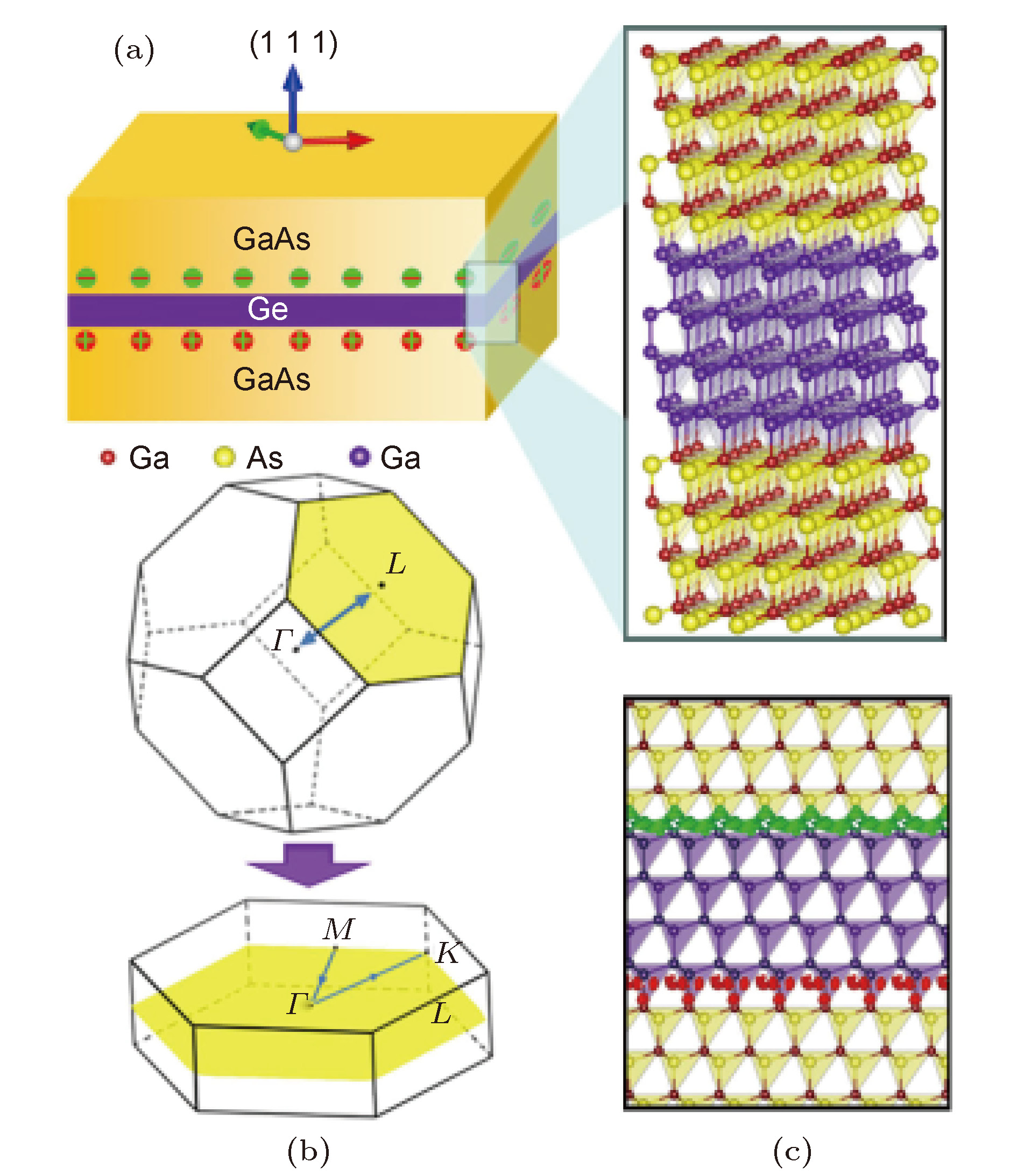
图 5 (a) GaAs/Ge/GaAs[111]量子阱示意图, (b)布里渊区折叠示意图, (c) GaAs/Ge/GaAs[111]量子阱上下极性界面电荷积累示意图.
Figure 5. (a) Schematic of the structure of an ultrathin Ge layer sandwiched by thick GaAs layers (the upper left-hand panel). The upper right-hand panel amplifies the atomic configuration of the GaAs/Ge/GaAs quantum well containing four bilayer Ge. Notice that the Ga and As atoms locate at the opposite interfaces which leads to a charge accumulation schematically shown in the left-hand panel. (b) the BZ of bulk Ge and the folded BZ of GaAs = Ge = GaAs QW along the [111] crystallographic direction. (c) the charge accumulation at two opposite interfaces obtained from the first-principles calculation. The red and green isosurfaces describe the positive and negative charge accumulations at opposite interfaces.
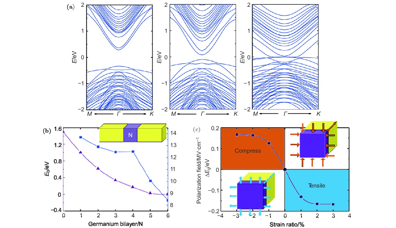
图 6 不同Ge层厚GaAs/Ge/GaAs[111]量子阱的带隙, (a)从左至右分别对应Ge层厚为2、4个双原子层以及4个双原子层量子阱并考虑3%平面内张应力情况. 左下(b)为量子阱能隙以及內建电场大小随Ge层厚增加的变化关系. (d)平面内应力对能隙的改变.
Figure 6. (a) Band structures of GaAs/Ge/GaAs sandwiched structures with different Ge portions obtained from the first-principles HSE calculations. From left to right, two Ge bilayers, four Ge bilayers, and four Ge bilayers with 3% in-plane tensile strain. (b) the band gap (purple line with diamonds) and the inner polarization field strength (blue line with squares) as functions of the number of Ge bilayers. (c) the variation of band gap Eg = Estrain g-Eg as a function of in-plane strain.
图 7 (a)从30带k.p模型获得的具有18Å 的Ge层厚度的GaAs/Ge/GaAs QW结构的能带结构. 插图显示了电子, 重空穴(HH)和轻空穴(LH)的Rashba自旋分裂(RSS). (b)通过求解有效四带模型得到的量子线的能带结构. 无能隙的边缘态由图中的红线表示. 中心插图显示了量子线的示意图和螺旋边缘态. 右(红色)和左峰(蓝色)分别描述了在k|| = -0.01Å-1处的自旋向上和自旋向下边缘状态的密度分布.
Figure 7. (a) Band structures of a GaAs/Ge/GaAs QW structure with 18 Å Ge layer thickness obtained from the 30-band k.p model. The inset shows the Rashba spin splitting (RSS) of electron, heavy hole (HH), and light hole (LH). (b) Band structure of the quantum wire obtained by solving the effective four-band model. The gapless edge states are shown by the red line. The central inset shows the schematic of the quantum wire and the helical edge states. The right (red) and left peaks (blue) describe the density distribution of the spin-up and spin-down edge states at k|| = -0.01Å-1, respectively.
-
[1] Klitzing K V, Dorda G, Pepper M 1980 Physical Review Letters 45 494
 Google Scholar
[2] Tsui D C, Stormer H L, Gossard A C 1982 Physical Review Letters 48 1559
 Google Scholar
[3] Haldane F D M 1988 Physical Review Letters 61 2015
 Google Scholar
[4] Chang C Z, Zhang J, Feng X, Shen J, Zhang Z, Guo M, Li K, Ou Y, Wei P, Wang L L, Ji Z Q, Feng Y, Ji S, Chen X, Jia J, Dai X, Fang Z, Zhang S C, He K, Wang Y, Lu L, Ma X C, Xue Q K 2013 Science 340 167
 Google Scholar
[5] Hasan M Z, Kane C L 2010 Rev. Mod. Phys. 82 3045
 Google Scholar
[6] He Q L, Pan L, Stern A L, Burks E C, Che X, Yin G, Wang J, Lian B, Zhou Q, Choi E S, Murata K, Kou X, Chen Z, Nie T, Shao Q, Fan Y, Zhang S C, Liu K, Xia J, Wang K L 2017 Science 357 294
 Google Scholar
[7] Weng H, Fang C, Fang Z, Bernevig B A, Dai X 2015 Physical Review X 5 011029
[8] Yoshida S, Misawa S, Gonda S 1983 Appl. Phys. Lett. 42 427
 Google Scholar
[9] Amano H, Sawaki N, Akasaki I, Toyoda Y 1986 Appl. Phys. Lett. 48 353
 Google Scholar
[10] Asif Khan M, Kuznia J N, Olson D T, George T, Pike W T 1993 Appl. Phys. Lett. 63 3470
 Google Scholar
[11] Hwang H Y, Iwasa Y, Kawasaki M, Keimer B, Nagaosa N, Tokura Y 2012 Nat. Mater. 11 103
 Google Scholar
[12] Natural Editorial 2012 Nat. Mater. 11 91
[13] Seibold G, Caprara S, Grilli M, Raimondi R 2017 Physical Review Letters 119 256801
 Google Scholar
[14] Kroemer H 2001 Rev. Mod. Phys. 73 783
 Google Scholar
[15] Bernardini F, Fiorentini V, Vanderbilt D 1997 Physical Review B 56 R10024
 Google Scholar
[16] Xia J-B 1989 Physical Review B 40 8500
 Google Scholar
[17] 夏建白, 朱邦芬 1995 半导体超晶格物理 (上海: 上海科学技术出版社)
Xia J B, Zhu B F 1995 Semiconductor Superlattice Physics(Shanghai: Shanghai Scientific & Technical Publishers) (in Chinese)
[18] 褚君浩 2005 窄禁带半导体物理学 (1 Ed.) (北京: 科学出版社)
Chu J H 2005 Narrow Gap Semiconductor Physics (1 Ed.) (Beijing: Science Press) (in Chinese)
[19] Miao M S, Yan Q, Van de Walle C G, Lou W K, Li L L, Chang K 2012 Phys. Rev. Lett. 109 186803
 Google Scholar
[20] Bernevig B A, Hughes T L, Zhang S C 2006 Science 314 1757
 Google Scholar
[21] Nitta J, Akazaki T, Takayanagi H, Enoki T 1997 Physical Review Letters 78 1335
 Google Scholar
[22] Grundler D 2000 Phys. Rev. Lett. 84 6074
 Google Scholar
[23] Winkler R 2003 Spin-Orbit Coupling Effects in Two-Dimensional Electron and Hole Systems (Springer)
[24] Zawadzki W, Pfeffer P 2004 Semicond. Sci. Technol. 19 R1
 Google Scholar
[25] Yang W, Chang K, Zhang S C 2008 Phys. Rev. Lett. 100 056602
 Google Scholar
[26] Li J, Chang K 2009 Appl. Phys. Lett. 95 222110
 Google Scholar
[27] Li J, Yang W, Chang K 2009 Phys. Rev. B 80 035303
 Google Scholar
[28] Qi X L, Zhang S C 2011 Rev. Mod. Phys. 83 1057
 Google Scholar
[29] Knez I, Du R-R, Sullivan G 2011 Phys. Rev. Lett. 107 136603
 Google Scholar
[30] Mishra U K, Shen L, Kazior T E, Yi-Feng W 2008 Proceedings of the IEEE 96 287
 Google Scholar
[31] Songbek C, Akihiko Y, Hiroshi W, Yoshihiro I, Akihiko Y 2009 Appl. Phys. Express 2 021001
 Google Scholar
[32] Pan W, Dimakis E, Wang G T, Moustakas T D, Tsui D C 2014 Appl. Phys. Lett. 105 213503
 Google Scholar
[33] 蒋维栋, 张翔九, 王迅 1989 物理 18 205
Jiang W D, Zang X J, Wang X 1989 Acta Phys. Sin. 18 205
[34] Zhang D, Lou W, Miao M, Zhang S-c, Chang K 2013 Phys. Rev. Lett. 111 156402
 Google Scholar
Catalog
Metrics
- Abstract views: 19862
- PDF Downloads: 378
- Cited By: 0


 DownLoad:


