-
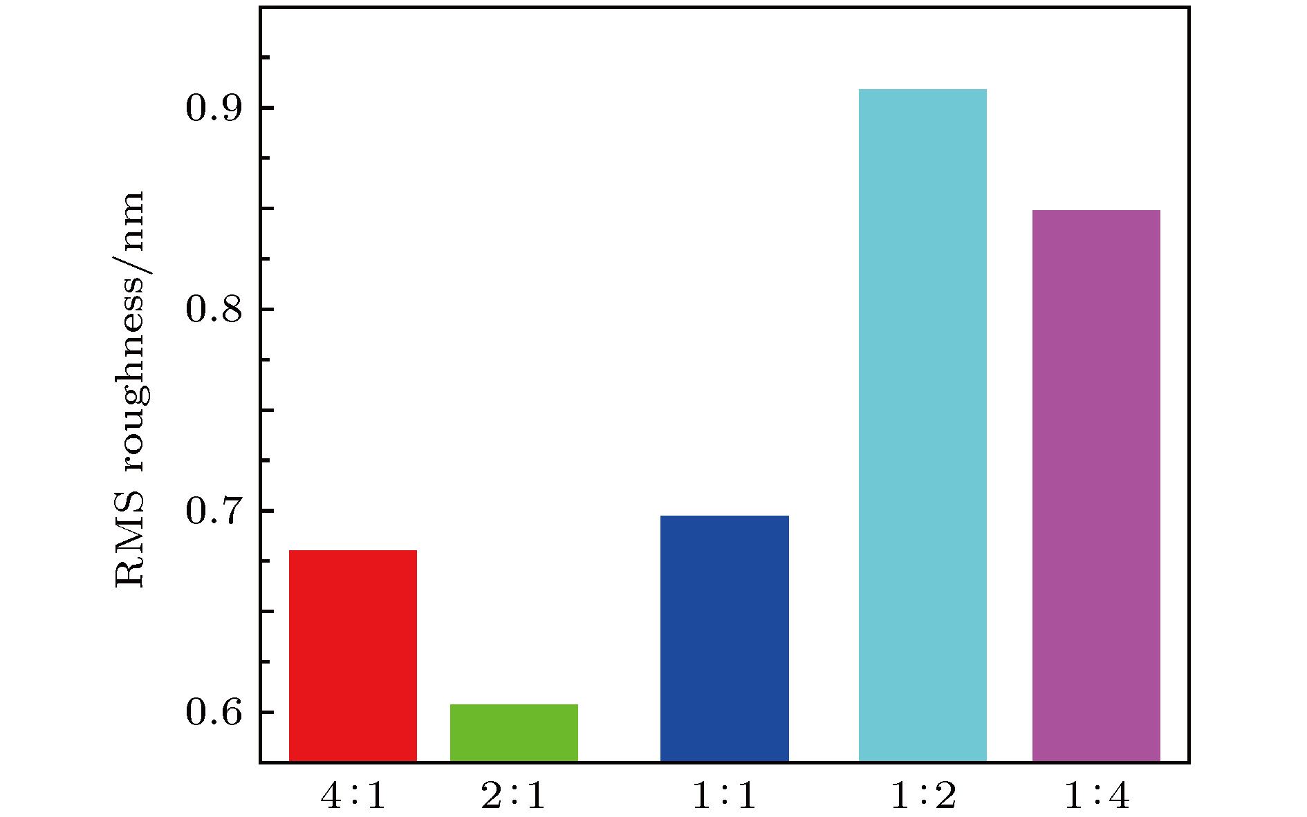
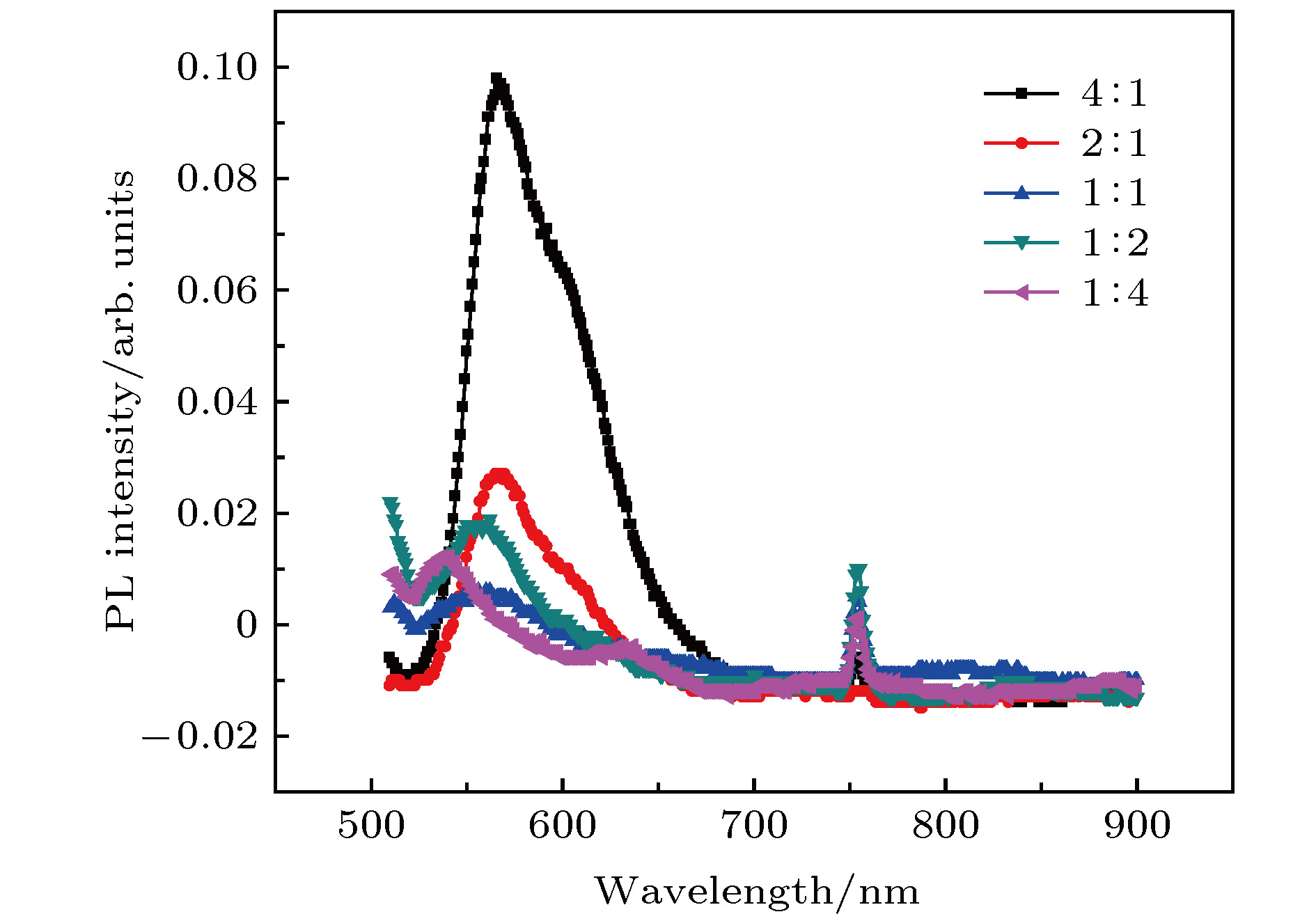
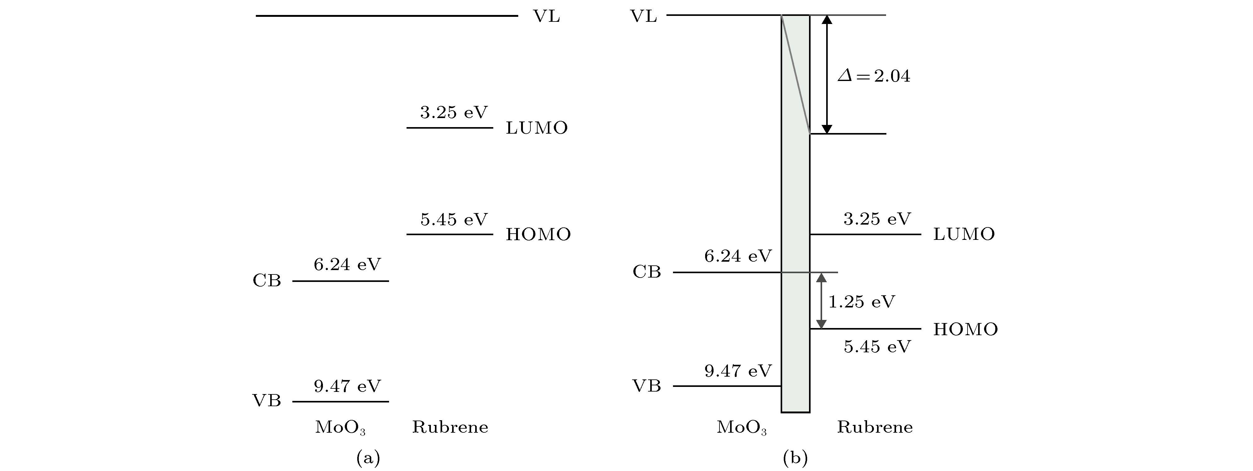
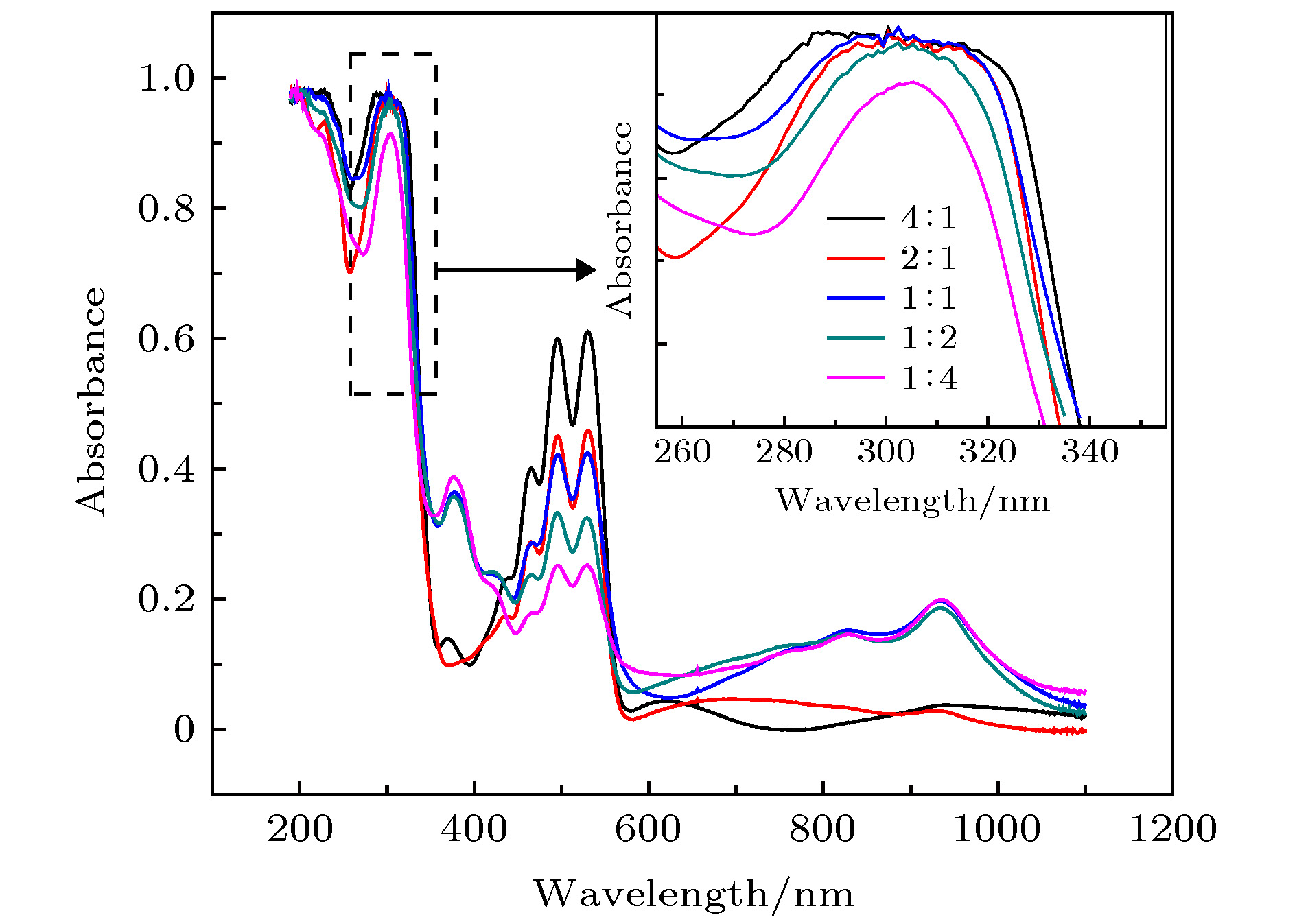
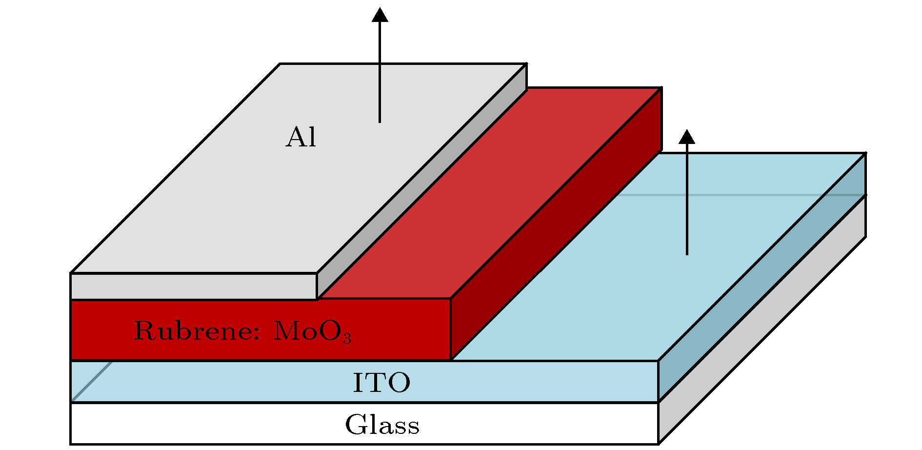
In this paper, the mixed films with different rubrene-to-MoO3 ratios are deposited on the substrates of Si, indium tin oxide and quartz glass by using the thermal evaporation technique. First, these films are characterized by atomic force microscopy and X-ray diffraction in order to identify their surface morphology and their structure properties. The results show that all the films are amorphous and the film has the best flatness when the rubrene-to-MoO3 ratio is 2∶1. Second, the optical properties of the mixed films are investigated by both photoluminescence (PL) spectra and absorption spectra. The optical band gap of rubrene and MoO3 are 2.2 eV and 3.49 eV respectively and there is almost no absorption about rubrene and MoO3 in the near-infrared (NIR) region. However the PL spectrum shows a peak in NIR region and it indicates that the interface between rubrene and MoO3 possesses an abrupt discontinuity at the vacuum level, resulting in electron wave functions overlapping and charge-transfer complex (CTC) forming. The intermediate state within the original band gap of rubrene with energy of 1.25 eV is induced by the CTC, which suggests the possibility of charge transfer exciton generated upon NIR excitation. The absorption spectra of the mixed films show that there is an obvious absorption. All the films have the same absorption peak except the film with a rubrene-to-MoO3 ratio of 4∶1 and it indicates that the concentration of MoO3 has almost no influence on the absorption of the mixed films. The optical band gaps of the mixed thin films are calculated in a spectral range of 345-1035 nm according to the Tauc equation, and the results show that the optical band gap of the film with a rubrene-to-MoO3 ratio of 2∶1 is narrowest (~2.23 eV). In order to study the electrical characteristics of the mixed films, an Al/rubrene:MoO3/ITO device is fabricated. The current density-voltage (J-V) characteristic is also investigated. The analysis of the J-V measurement for the device indicates that the current conduction in the Al/rubrene:MoO3/ITO device is Ohmic type when the rubrene-to-MoO3 ratios are 4∶1 and 2∶1, and it is Schottky type when the ratio is other value. The current for rubrene-to-MoO3 ratio of 1∶1 is larger than that for 1∶2, which indicates that the contact is better when the surface is more smooth. These properties of the mixed films can result in the applications in the near-infrared region. -
Keywords:
- mixed film of rubrene∶MoO3 /
- atomic force microscope /
- X-ray diffraction /
- properties of optical and electrical
[1] Sundar V C, Zaumseil J, Podzorov V, et al. 2004 Science 303 1644
 Google Scholar
[2] Luo Y, Brun M, Rannou P, et al. 2007 Phys. Status Solidi 204 1851
 Google Scholar
[3] Park S W, Jeong S H, Choi J M, et al. 2007 Appl. Phys. Lett. 91 26
[4] 邓金祥, 康成龙, 杨冰, 等 2012 真空科学与技术学报 32 678
 Google Scholar
Deng J X, Kang C L, Yang B, et al. 2012 Chin. J. Vacu. Sci. Tech. 32 678
 Google Scholar
[5] Ng T W, Lo M F, Yang Q D, et al. 2012 Adv. Func. Mater. 22 3035
 Google Scholar
[6] Liu Y, Wu X M, Xiao Z H, et al. 2017 Appl. Surf. Sci. 413 302
 Google Scholar
[7] Hsu C H, Deng J, Staddon C R, et al. 2007 Appl. Phys. Lett. 91 193505
 Google Scholar
[8] Matsushima T, Jin G H, Kanai Y, et al. 2011 Org. Elec. 12 520
 Google Scholar
[9] Kubo M, Iketaki K, Kaji T, et al. 2011 Appl. Phys. Lett. 98 40
[10] Nakanotani H, Kakizoe H, Adachi C 2011 Sol. Sta. Com. 151 93
 Google Scholar
[11] 杨海刚, 尤天友, 宋桂林, 等 2011 真空 48 58
 Google Scholar
Yang H G, You T Y, Song J L, et al. 2011 Vacuum 48 58
 Google Scholar
[12] 王娜娜, 于军胜, 王琦, 等 2011 量子电子学报 28 191
 Google Scholar
Wang N N, Yu J S, Wang Q, et al. 2011 Chin. J. Quan. Elec. 28 191
 Google Scholar
[13] 刘恩科, 朱秉生, 罗晋生 2017 半导体物理学 (第七版) (北京: 电子工业出版社) 第201页
Liu E K, Zhu B S, Luo J S 2017 The Physics Semiconductors E7 (Beijing: Publishing House of Electronics Industry) p201 (in Chinese)
[14] 李林娜,陈新亮,刘晨等 2010 光电子·激光 21 4
 Google Scholar
Li L N, Chen X L, Liu C, et al. 2010 Journal of Optoelectronics·Laser 21 4
 Google Scholar
[15] 冯丽萍, 刘正堂 2008 材料开发与应用 23 5
 Google Scholar
Feng L P, Liu Z T 2008 Devel. Appl. Mater. 23 5
 Google Scholar
[16] 吴伟杰 2016 硕士学位论文 (成都: 电子科技大学)
Wu W J 2016 M. S. Thesis (Chengdu: University of Electronic Science and Technology of China) (in Chinese)
[17] Arfaoui A, Mhamdi A, Besrour N, et al. 2018 Thin Solid Films 648 12
 Google Scholar
[18] He X X, Chow W L, Liu F C, et al. 2017 Small 13 1602558
 Google Scholar
[19] El-Nahass M M, Farag A M, Abd El-Rahman K F, et al. 2005 Opt. Laser Technol. 37 513
 Google Scholar
[20] Ambily S, Menon C S 1999 Thin Solid Films 347 284
 Google Scholar
[21] Farag A A M, Yahia I S 2010 Opt. Commun. 283 4310
 Google Scholar
[22] Petrenko T, Krylova O, Neese F, et al. 2009 New J. Phys. 11 1367
 Google Scholar
[23] Mitrofanov O, Lang D V, Kloc C, et al. 2006 Phys. Rev. Lett. 97 166601
 Google Scholar
[24] Tavazzi S, Borghesi A, Papagni A, et al. 2007 Phys. Rev. B 75 245416
 Google Scholar
[25] Tuğluoğlu N, Barış B, Gürel H, et al. 2014 J. Alloy Compd. 582 696
 Google Scholar
[26] 伍春燕, 钟韶, 陈易明等 2002 光谱学与光谱分析 22 495
 Google Scholar
Wu C Y, Zhong S, Chen Y M, et al. 2002 Spec. Spec. Anal. 22 495
 Google Scholar
-
Rubrene∶MoO3 4∶1 2∶1 1∶1 1∶2 1∶4 能隙Eg/eV 2.24 2.23 2.25 2.25 2.25 -
[1] Sundar V C, Zaumseil J, Podzorov V, et al. 2004 Science 303 1644
 Google Scholar
[2] Luo Y, Brun M, Rannou P, et al. 2007 Phys. Status Solidi 204 1851
 Google Scholar
[3] Park S W, Jeong S H, Choi J M, et al. 2007 Appl. Phys. Lett. 91 26
[4] 邓金祥, 康成龙, 杨冰, 等 2012 真空科学与技术学报 32 678
 Google Scholar
Deng J X, Kang C L, Yang B, et al. 2012 Chin. J. Vacu. Sci. Tech. 32 678
 Google Scholar
[5] Ng T W, Lo M F, Yang Q D, et al. 2012 Adv. Func. Mater. 22 3035
 Google Scholar
[6] Liu Y, Wu X M, Xiao Z H, et al. 2017 Appl. Surf. Sci. 413 302
 Google Scholar
[7] Hsu C H, Deng J, Staddon C R, et al. 2007 Appl. Phys. Lett. 91 193505
 Google Scholar
[8] Matsushima T, Jin G H, Kanai Y, et al. 2011 Org. Elec. 12 520
 Google Scholar
[9] Kubo M, Iketaki K, Kaji T, et al. 2011 Appl. Phys. Lett. 98 40
[10] Nakanotani H, Kakizoe H, Adachi C 2011 Sol. Sta. Com. 151 93
 Google Scholar
[11] 杨海刚, 尤天友, 宋桂林, 等 2011 真空 48 58
 Google Scholar
Yang H G, You T Y, Song J L, et al. 2011 Vacuum 48 58
 Google Scholar
[12] 王娜娜, 于军胜, 王琦, 等 2011 量子电子学报 28 191
 Google Scholar
Wang N N, Yu J S, Wang Q, et al. 2011 Chin. J. Quan. Elec. 28 191
 Google Scholar
[13] 刘恩科, 朱秉生, 罗晋生 2017 半导体物理学 (第七版) (北京: 电子工业出版社) 第201页
Liu E K, Zhu B S, Luo J S 2017 The Physics Semiconductors E7 (Beijing: Publishing House of Electronics Industry) p201 (in Chinese)
[14] 李林娜,陈新亮,刘晨等 2010 光电子·激光 21 4
 Google Scholar
Li L N, Chen X L, Liu C, et al. 2010 Journal of Optoelectronics·Laser 21 4
 Google Scholar
[15] 冯丽萍, 刘正堂 2008 材料开发与应用 23 5
 Google Scholar
Feng L P, Liu Z T 2008 Devel. Appl. Mater. 23 5
 Google Scholar
[16] 吴伟杰 2016 硕士学位论文 (成都: 电子科技大学)
Wu W J 2016 M. S. Thesis (Chengdu: University of Electronic Science and Technology of China) (in Chinese)
[17] Arfaoui A, Mhamdi A, Besrour N, et al. 2018 Thin Solid Films 648 12
 Google Scholar
[18] He X X, Chow W L, Liu F C, et al. 2017 Small 13 1602558
 Google Scholar
[19] El-Nahass M M, Farag A M, Abd El-Rahman K F, et al. 2005 Opt. Laser Technol. 37 513
 Google Scholar
[20] Ambily S, Menon C S 1999 Thin Solid Films 347 284
 Google Scholar
[21] Farag A A M, Yahia I S 2010 Opt. Commun. 283 4310
 Google Scholar
[22] Petrenko T, Krylova O, Neese F, et al. 2009 New J. Phys. 11 1367
 Google Scholar
[23] Mitrofanov O, Lang D V, Kloc C, et al. 2006 Phys. Rev. Lett. 97 166601
 Google Scholar
[24] Tavazzi S, Borghesi A, Papagni A, et al. 2007 Phys. Rev. B 75 245416
 Google Scholar
[25] Tuğluoğlu N, Barış B, Gürel H, et al. 2014 J. Alloy Compd. 582 696
 Google Scholar
[26] 伍春燕, 钟韶, 陈易明等 2002 光谱学与光谱分析 22 495
 Google Scholar
Wu C Y, Zhong S, Chen Y M, et al. 2002 Spec. Spec. Anal. 22 495
 Google Scholar
Catalog
Metrics
- Abstract views: 12793
- PDF Downloads: 111
- Cited By: 0


 DownLoad:
