


-
本文对第四代双沟槽型碳化硅场效应晶体管开展了不同栅极偏置电压下的60Co-γ辐照实验, 并在辐照后进行了室温退火实验. 实验结果表明, 辐照后器件的阈值电压负向漂移, 且在正向栅极偏压下电学性能退化尤为明显. 通过分析器件的1/f噪声特性发现, 在不同栅极偏置条件下辐照后器件的漏极电流噪声归一化功率谱密度升高了4—9个数量级, 这表明辐照后器件内部缺陷密度显著增加. 对辐照后器件进行了24, 48和168 h的室温退火实验, 退火后器件阈值电压有所升高, 表明器件的电学性能在室温下可以部分恢复, 主要因为辐照产生的浅氧化物陷阱电荷在室温下退火, 而深氧化物陷阱电荷和界面陷阱电荷在室温难以恢复. 结合TCAD仿真模拟进一步分析器件总剂量效应微观机制. 结果表明, 辐照在氧化层中诱生的大量氧化物陷阱电荷造成栅极氧化层中靠近沟道一侧的电场强度增大, 导致器件的阈值电压负向漂移, 影响器件性能.In this work, the influence of 60Co-γ ray irradiation on double trench SiC metal–oxide–semiconductor field-effect transistors (MOSFETs) is investigated under different conditions. First, the effects of the total ionizing dose (TID) on the electrical performance of the device at different gate bias voltages are studied. The results indicate that at 150 krad(Si) irradiation dose, the threshold voltage of the device after being irradiated decreases by 3.28 and 2.36 V for gate voltages of +5 and –5 V bias, respectively, whereas the threshold voltage of the device after being irradiated decreases by only 1.36 V for a gate voltage of 0 V bias. The threshold voltage of the device after irradiation drifts in the negative direction, and the degradation of the electrical performance is especially obvious under the positive gate bias. This is attributed to the increase in the number of charges trapped in the oxide layer. At the same time, room temperature annealing experiments are performed on the irradiated devices for 24, 48, and 168 h. The shallow oxide trap charges generated by irradiation are annealed at room temperature, while the deep oxide trap charges and interface trap charges are difficult to recover at room temperature, resulting in an increase in the threshold voltage of the devices after being annealed, indicating that the electrical properties of the devices can be partially recovered after being annealed at room temperature. In order to characterize the effect of 60Co-γ ray irradiation on the interfacial state defect density of the devices, low frequency noise (1/f ) tests are performed at different doses and different gate bias voltages. The 1/f low frequency noise testing shows that under different bias voltages, the density of irradiation defects in the device increases due to the presence of induced oxide trap charges in the oxide layer of the device after being irradiated and the interfacial trap charges generated at the SiO2/SiC interface. This results in an increase of 4–9 orders of magnitude in the normalized power spectral density of the drain current noise of the irradiated device. To further ascertain the irradiation damage mechanism of the device, a numerical simulation is carried out using the TCAD simulation tool, and the results show that a large number of oxide trap charges induced by irradiation in the oxide layer cause an increase in the electric field strength in the gate oxide layer close to the trench side, which leads to a negative drift of the threshold voltage of the device and affects the performance of the device. The results of this work can provide important theoretical references for investigating the radiation effect mechanism and designing the anti radiation reinforcement of double trench SiC MOSFET devices.
-
Keywords:
- double-trench /
- silicon carbide /
- low-frequency noise /
- total ionizing dose effect
[1] Matsuda T, Yokoseki T, Mitomo S, Murata K, Makino T, Abe H, Takeyama A, Onoda S, Tanaka Y, Kandori M, Yoshie T, Hijikata Y, Ohshima T 2016 Mater. Sci. Forum 858 860
 Google Scholar
[2] Murata K, Mitomo S, Matsuda T, Yokoseki T, Makino T, Onoda S, Takeyama A, Ohshima T, Okubo S, Tanaka Y, Kandori M, Yoshie T, Hijikata Y 2017 Phys. Status Solidi A 214 1600446
Google Scholar
[3] Ohshima T, Yoshikawa M, Itoh H, Aoki Y, Nashiyama I 1999 Mater. Sci. Eng., B 61–62 480
[4] Takeyama A, Makino T, Okubo S, Tanaka Y, Yoshie T, Hijikata Y, Ohshima T 2019 Materials 12 2741
Google Scholar
[5] Dimitrijev S, Jamet P 2003 Microelectron. Reliab. 43 225
Google Scholar
[6] Liu J, Lu J, Tian X, Chen H, Bai Y, Liu X 2020 Electron. Lett. 56 1273
Google Scholar
[7] Pappis D, Zacharias P 2017 2017 19th European Conference on Power Electronics and Applications (EPE’17 ECCE Europe) Warsaw, Poland, September 11–14, 2017 p2017-12-14
[8] Sato I, Tanaka T, Hori M, Yamada R, Toba A, Kubota H 2021 Electr. Eng. Jpn. 214 e23323
Google Scholar
[9] Winokur P S, Schwank J R, McWhorter P J, Dressendorfer P V, Turpin D C 1984 IEEE Trans. Nucl. Sci. 31 1453
Google Scholar
[10] Akturk A, McGarrity J M, Potbhare S, Goldsman N 2012 IEEE Trans. Nucl. Sci. 59 3258
Google Scholar
[11] Popelka S, Hazdra P 2016 Mater. Sci. Forum 858 856
Google Scholar
[12] Yu Q, Ali W, Cao S, Wang H, Lv H, Sun Y, Mo R, Wang Q, Mei B, Sun J, Zhang H, Tang M, Bai S, Zhang T, Bai Y, Zhang C 2022 IEEE Trans. Nucl. Sci. 69 1127
Google Scholar
[13] Sampath M, Morisette D, Cooper J 2018 Mater. Sci. Forum 924 752
Google Scholar
[14] 顾朝桥, 郭红霞, 潘霄宇, 雷志峰, 张凤祁, 张鸿, 琚安安, 柳奕天 2021 70 166101
Google Scholar
Gu Z Q, Guo H X, Pan X Y, Lei Z F, Zhang F Q, Zhang H, Ju A A, Liu Y T 2021 Acta Phys. Sin. 70 166101
Google Scholar
[15] 陈伟华, 杜磊, 庄奕琪, 包军林, 何亮, 张天福, 张雪 2009 58 4090
Google Scholar
Chen W H, Du L, Zhuang Y Q, Bao J L, He L, Zhang T F, Zhang X 2009 Acta Phys. Sin. 58 4090
Google Scholar
[16] 刘张李, 胡志远, 张正选, 邵华, 宁冰旭, 毕大炜, 陈明, 邹世昌 2011 60 116103
Google Scholar
Liu Z L, Hu Z Y, Zhang Z X, Shao H, Ning B X, Bi D W, Chen M, Zou S C 2011 Acta Phys. Sin. 60 116103
Google Scholar
[17] Oldham T R, McLean F B 2003 IEEE Trans. Nucl. Sci. 50 483
Google Scholar
[18] 孟洋 2024 硕士学位论文学位论文 (扬州: 扬州大学)
Meng Y 2024 M. S. Thesis (Yangzhou: Yang Zhou University
[19] 万欣 2017 博士学位论文学位论文 (北京: 清华大学)
Wan X 2016 Ph. D. Dissertation (Beijing: Tsinghua University
[20] Fleetwood D M, Winokur P S, Schwank J R 1988 IEEE Trans. Nucl. Sci. 35 1497
Google Scholar
[21] Shaneyfelt M R, Schwank J R, Fleetwood D M, Winokur P S, Hughes K L, Sexton F W 1990 IEEE Trans. Nucl. Sci. 37 1632
Google Scholar
[22] McWhorter P J, Winokur P S 1986 Appl. Phys. Lett. 48 133
Google Scholar
[23] Mitomo S, Matsuda T, Murata K, Yokoseki T, Makino T, Takeyama A, Onoda S, Ohshima T, Okubo S, Tanaka Y, Kandori M, Yoshie T, Hijikata Y 2017 Phys. Status Solidi A 214 1600425
Google Scholar
[24] Scofield J H, Fleetwood D M 1991 IEEE Trans. Nucl. Sci. 38 1567
Google Scholar
[25] Silvestri M, Uren M J, Killat N, Marcon D, Kuball M 2013 Appl. Phys. Lett. 103 043506
Google Scholar
[26] Wang J L, Chen Y Q, Feng J T, Xu X B, En Y F, Hou B, Gao R, Chen Y, Huang Y, Geng K W 2020 IEEE J. Electron Devices Soc. 8 145
Google Scholar
-
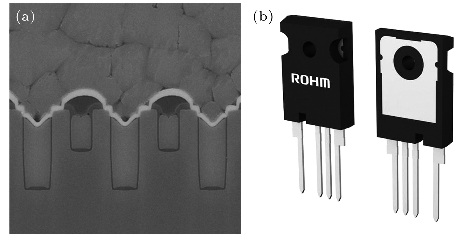
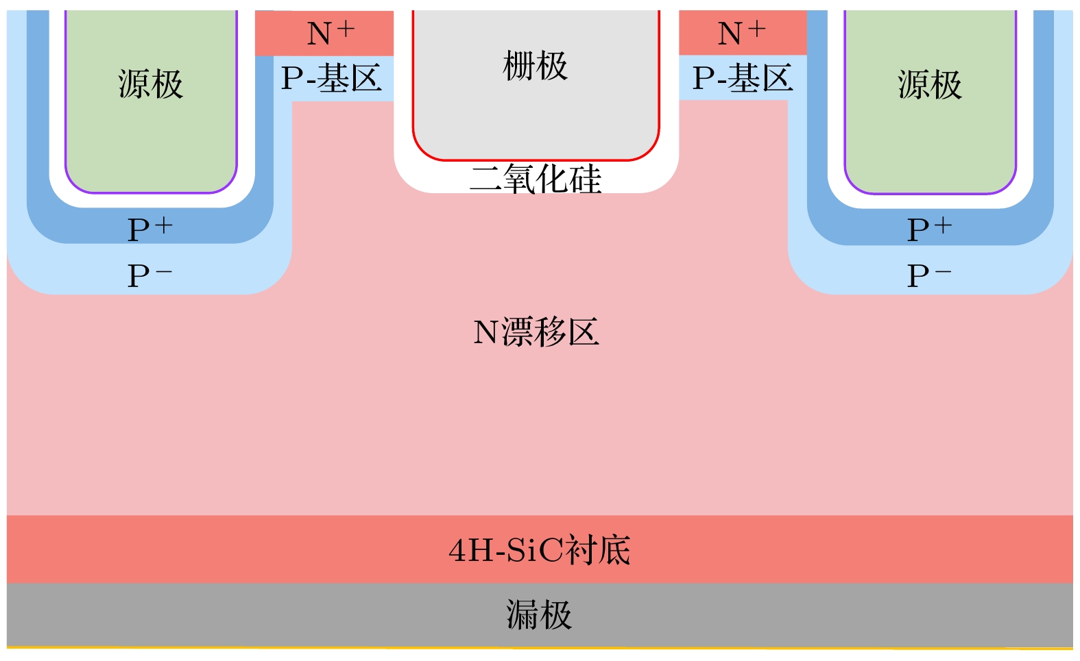
图 1 (a) SiC DTMOSFET单胞结构图; (b) 实际器件的照片
Fig. 1. (a) SiC DTMOSFET cell structure; (b) photo of real device.
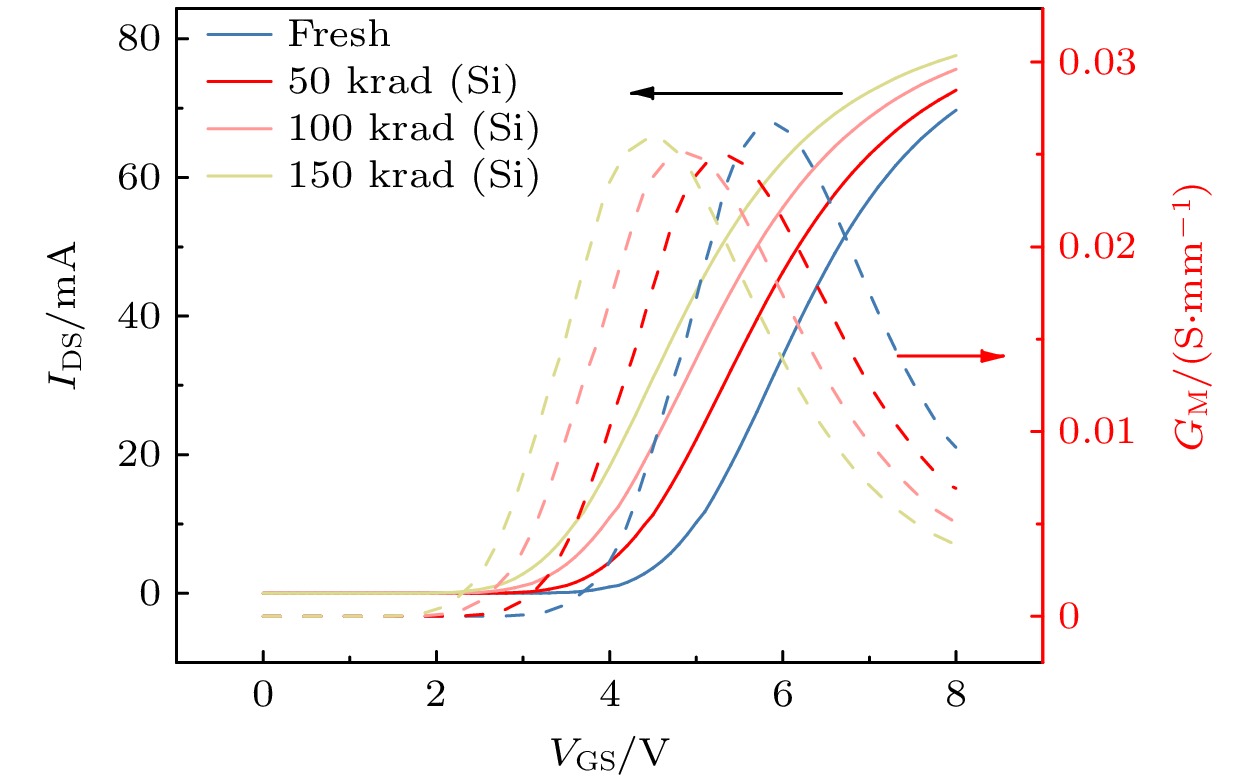
图 2 在VG = 0 V辐照条件下, SiC DTMOSFET的转移特性曲线随总剂量的变化趋势
Fig. 2. Under the irradiation condition of VG = 0 V, the transfer characteristic curve of SiC DTMOSFET changes with the total dose.
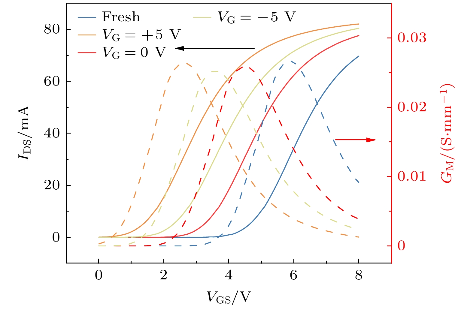
图 3 在剂量为150 krad(Si)辐照条件下, SiC DTMOSFET的转移特性曲线随栅极偏压的变化趋势
Fig. 3. Transfer characteristic curves of SiC DTMOSFET varies with gate bias under the irradiation dose of 150 krad(Si).
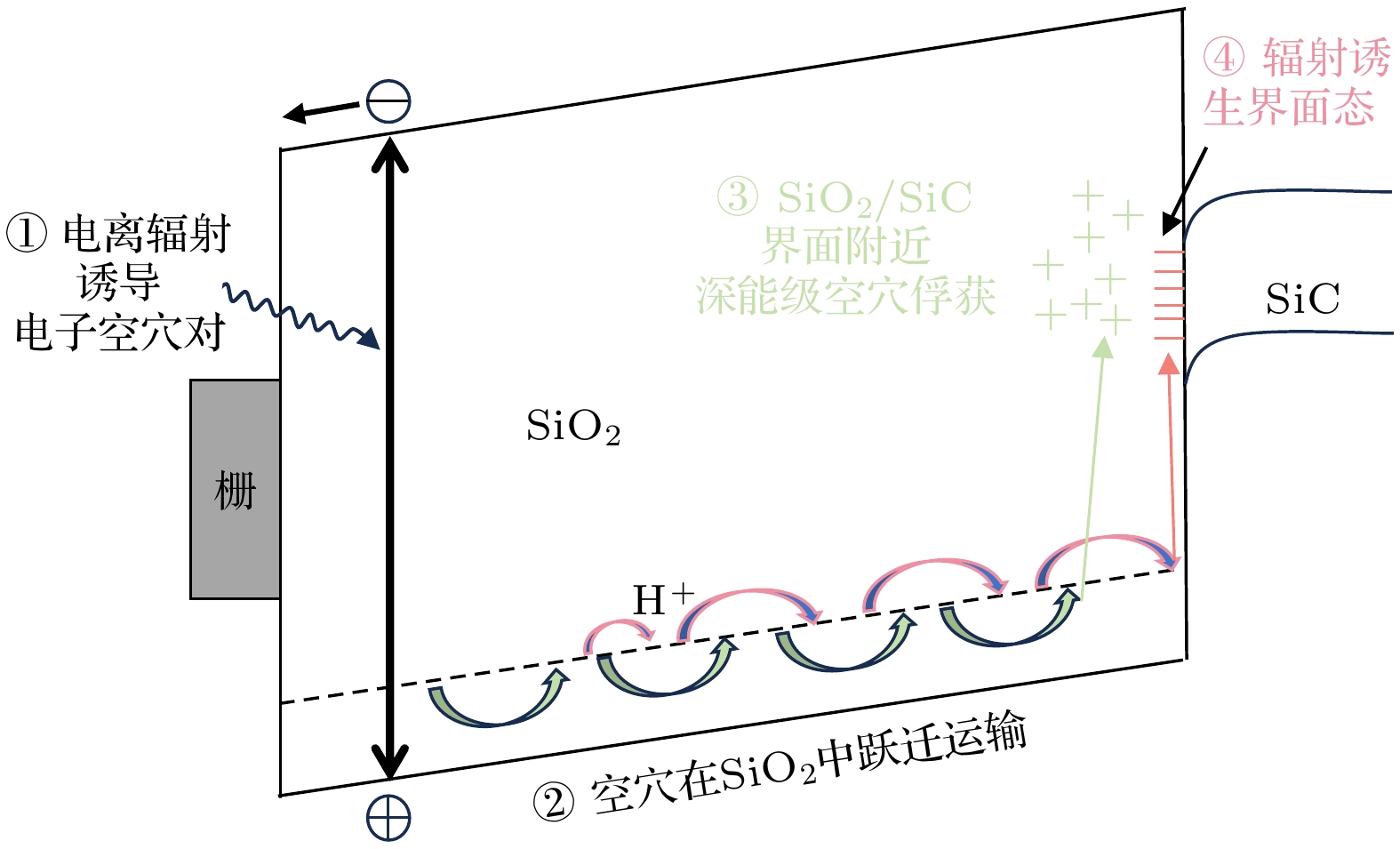
图 4 辐照后器件性能退化物理机制
Fig. 4. Physical mechanism of device performance degradation after irradiation.

图 5 SiC DTMOSFET的低频噪声特性 (a) 在VG = 0 V辐照条件下SiC DTMOSFET的低频噪声特性随总剂量的变化趋势; (b) 剂量为150 krad(Si)辐照条件下SiC DTMOSFET的低频噪声特性随栅极偏压的变化趋势
Fig. 5. Low frequency noise characteristics of SiC DTMOSFET: (a) The variation trend of low frequency noise characteristics of SiC DTMOSFET with total dose under VG = 0 V irradiation; (b) the variation trend of low-frequency noise characteristics of SiC DTMOSFET with gate bias under the irradiation dose of 150 krad(Si).
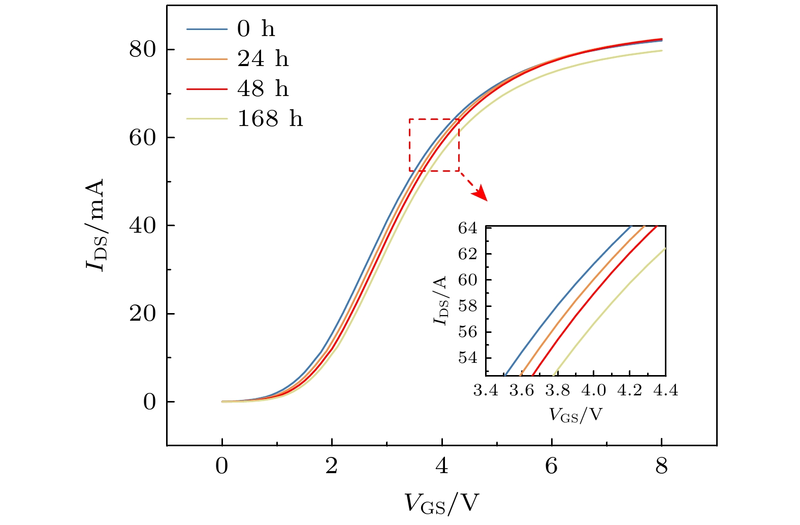
图 6 SiC DTMOSFET器件退火前后的转移特性(图中的子图为转移特性曲线局部放大图)
Fig. 6. Transfer characteristic of double-trench SiC MOSFET devices before and after annealing. The illustration in the figure is a partial enlargement of the transfer characteristic curve.
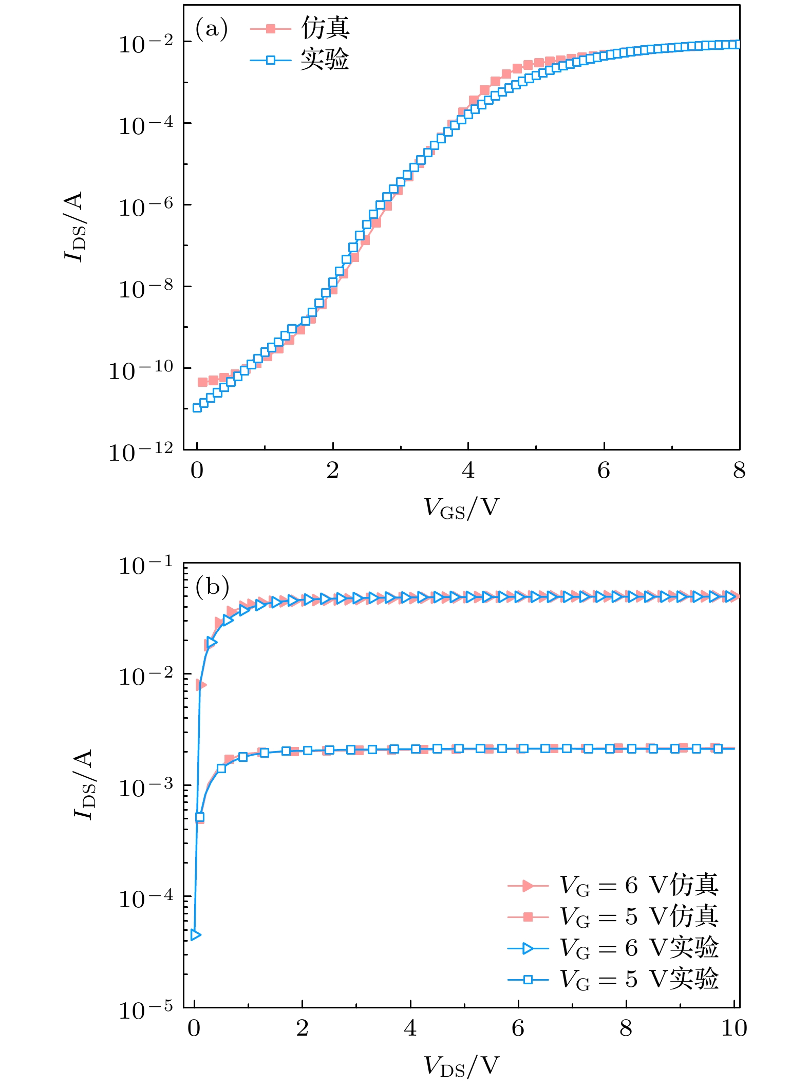
图 8 实验和TCAD仿真所得SiC DTMOSFET器件 (a)转移特性曲线; (b)输出特性曲线
Fig. 8. (a) Transfer characteristic curves; (b) output characteristic curves of SiC DTMOSFET device obtained by experiment and TCAD simulation.
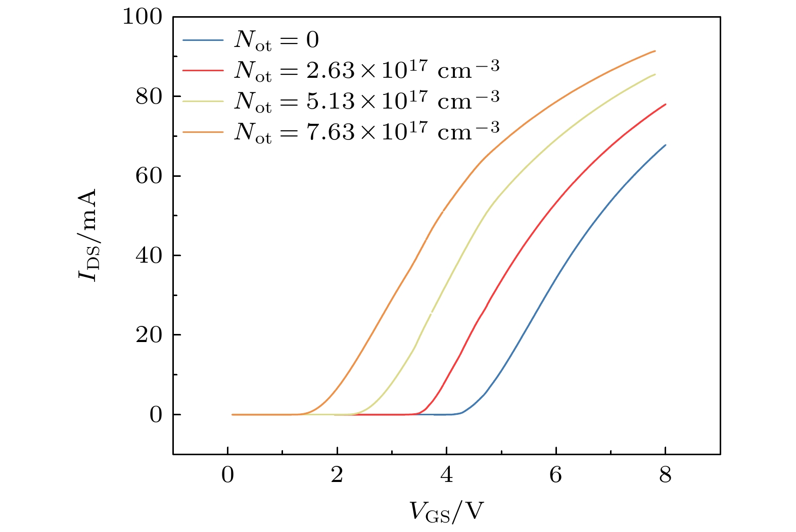
图 9 栅氧化层引入不同浓度的氧化物固定电荷造成SiC DTMOSFET器件转移特性曲线的漂移
Fig. 9. The gate oxide introduces different concentration of oxide fixed charge, which causes the drift of the transfer characteristic curve of SiC DTMOSFET device.
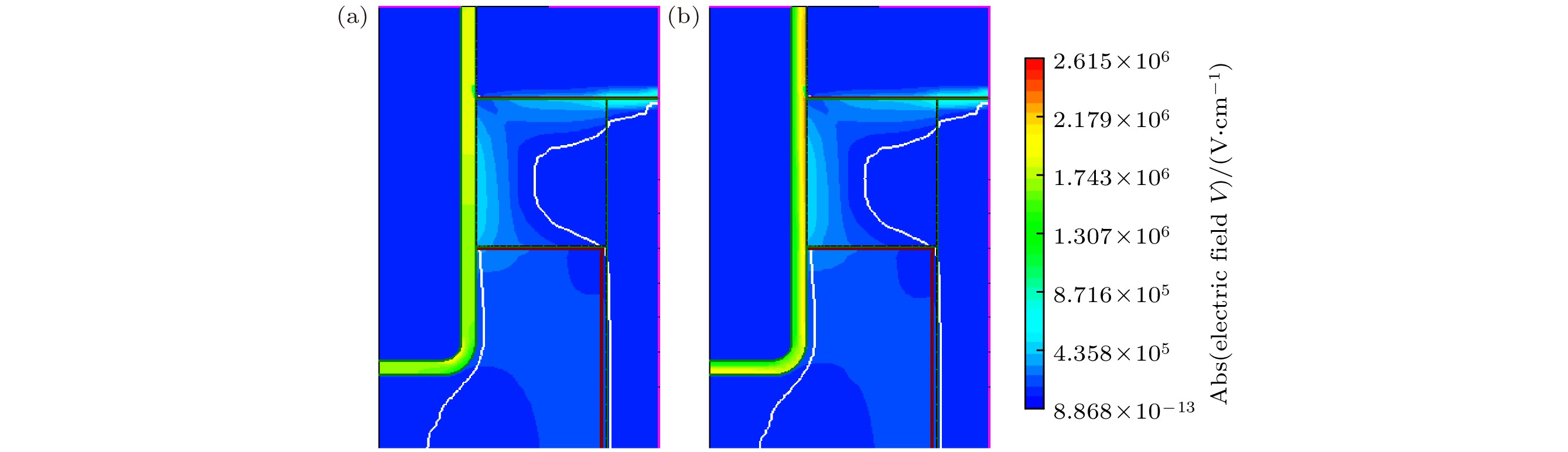
图 10 器件模型氧化层电场分布情况 (a) 引入氧化物陷阱电荷之前; (b)引入氧化物陷阱电荷之后
Fig. 10. Electric field distribution of oxide layer: (a) Before oxide trap charge injection; (b) after oxide trap charge injection.
表 1 不同栅极偏置电压和辐照剂量下SiC DTMOSFET器件的阈值电压变化量
Table 1. The amount of threshold voltage variation for double-trench SiC MOSFET devices with different gate voltages and irradiation doses.
实验条件 VG = 0 V VG = –5 V VG = +5 V 50 krad(Si) –0.58 V –1.27 V –1.52 V 100 krad(Si) –1.07 V –1.54 V –2.15 V 150 krad(Si) –1.36 V –2.36 V –3.28 V  下载: 导出CSV
表 2 辐照剂量为150 krad(Si)时不同栅极偏压下的氧化物陷阱电荷和界面态陷阱电荷密度
Table 2. The oxide trap charge density and interface trap charge density at different voltages when the irradiation dose is 150 krad(Si).
实验条件 VG = 0 V VG = –5 V VG = +5 V Not/(1010 cm–2) 7.63 12.70 20.10 Nit/(108 cm–2) 28.90 5.75 133.00
下载: 导出CSV
表 3 辐照剂量为150 krad(Si)时栅极氧化层中引入不同氧化物固定电荷密度下器件阈值电压变化量
Table 3. The threshold voltage variation of the device with different oxide fixed charge concentrations introduced into the gate oxide layer at the irradiation dose of 150 krad(Si).
$N_{\text{ot}}$/(1017 cm–3) 2.63 5.13 7.63 $\Delta V_{\text{th}}$/V –0.969 –1.902 –2.826
下载: 导出CSV
-
[1] Matsuda T, Yokoseki T, Mitomo S, Murata K, Makino T, Abe H, Takeyama A, Onoda S, Tanaka Y, Kandori M, Yoshie T, Hijikata Y, Ohshima T 2016 Mater. Sci. Forum 858 860
Google Scholar
[2] Murata K, Mitomo S, Matsuda T, Yokoseki T, Makino T, Onoda S, Takeyama A, Ohshima T, Okubo S, Tanaka Y, Kandori M, Yoshie T, Hijikata Y 2017 Phys. Status Solidi A 214 1600446
Google Scholar
[3] Ohshima T, Yoshikawa M, Itoh H, Aoki Y, Nashiyama I 1999 Mater. Sci. Eng., B 61–62 480
[4] Takeyama A, Makino T, Okubo S, Tanaka Y, Yoshie T, Hijikata Y, Ohshima T 2019 Materials 12 2741
Google Scholar
[5] Dimitrijev S, Jamet P 2003 Microelectron. Reliab. 43 225
Google Scholar
[6] Liu J, Lu J, Tian X, Chen H, Bai Y, Liu X 2020 Electron. Lett. 56 1273
Google Scholar
[7] Pappis D, Zacharias P 2017 2017 19th European Conference on Power Electronics and Applications (EPE’17 ECCE Europe) Warsaw, Poland, September 11–14, 2017 p2017-12-14
[8] Sato I, Tanaka T, Hori M, Yamada R, Toba A, Kubota H 2021 Electr. Eng. Jpn. 214 e23323
Google Scholar
[9] Winokur P S, Schwank J R, McWhorter P J, Dressendorfer P V, Turpin D C 1984 IEEE Trans. Nucl. Sci. 31 1453
Google Scholar
[10] Akturk A, McGarrity J M, Potbhare S, Goldsman N 2012 IEEE Trans. Nucl. Sci. 59 3258
Google Scholar
[11] Popelka S, Hazdra P 2016 Mater. Sci. Forum 858 856
Google Scholar
[12] Yu Q, Ali W, Cao S, Wang H, Lv H, Sun Y, Mo R, Wang Q, Mei B, Sun J, Zhang H, Tang M, Bai S, Zhang T, Bai Y, Zhang C 2022 IEEE Trans. Nucl. Sci. 69 1127
Google Scholar
[13] Sampath M, Morisette D, Cooper J 2018 Mater. Sci. Forum 924 752
Google Scholar
[14] 顾朝桥, 郭红霞, 潘霄宇, 雷志峰, 张凤祁, 张鸿, 琚安安, 柳奕天 2021 70 166101
Google Scholar
Gu Z Q, Guo H X, Pan X Y, Lei Z F, Zhang F Q, Zhang H, Ju A A, Liu Y T 2021 Acta Phys. Sin. 70 166101
Google Scholar
[15] 陈伟华, 杜磊, 庄奕琪, 包军林, 何亮, 张天福, 张雪 2009 58 4090
Google Scholar
Chen W H, Du L, Zhuang Y Q, Bao J L, He L, Zhang T F, Zhang X 2009 Acta Phys. Sin. 58 4090
Google Scholar
[16] 刘张李, 胡志远, 张正选, 邵华, 宁冰旭, 毕大炜, 陈明, 邹世昌 2011 60 116103
Google Scholar
Liu Z L, Hu Z Y, Zhang Z X, Shao H, Ning B X, Bi D W, Chen M, Zou S C 2011 Acta Phys. Sin. 60 116103
Google Scholar
[17] Oldham T R, McLean F B 2003 IEEE Trans. Nucl. Sci. 50 483
Google Scholar
[18] 孟洋 2024 硕士学位论文学位论文 (扬州: 扬州大学)
Meng Y 2024 M. S. Thesis (Yangzhou: Yang Zhou University
[19] 万欣 2017 博士学位论文学位论文 (北京: 清华大学)
Wan X 2016 Ph. D. Dissertation (Beijing: Tsinghua University
[20] Fleetwood D M, Winokur P S, Schwank J R 1988 IEEE Trans. Nucl. Sci. 35 1497
Google Scholar
[21] Shaneyfelt M R, Schwank J R, Fleetwood D M, Winokur P S, Hughes K L, Sexton F W 1990 IEEE Trans. Nucl. Sci. 37 1632
Google Scholar
[22] McWhorter P J, Winokur P S 1986 Appl. Phys. Lett. 48 133
Google Scholar
[23] Mitomo S, Matsuda T, Murata K, Yokoseki T, Makino T, Takeyama A, Onoda S, Ohshima T, Okubo S, Tanaka Y, Kandori M, Yoshie T, Hijikata Y 2017 Phys. Status Solidi A 214 1600425
Google Scholar
[24] Scofield J H, Fleetwood D M 1991 IEEE Trans. Nucl. Sci. 38 1567
Google Scholar
[25] Silvestri M, Uren M J, Killat N, Marcon D, Kuball M 2013 Appl. Phys. Lett. 103 043506
Google Scholar
[26] Wang J L, Chen Y Q, Feng J T, Xu X B, En Y F, Hou B, Gao R, Chen Y, Huang Y, Geng K W 2020 IEEE J. Electron Devices Soc. 8 145
Google Scholar


 下载:
下载:


计量
- 文章访问数: 1363
- PDF下载量: 44
- 被引次数: 0
