


-
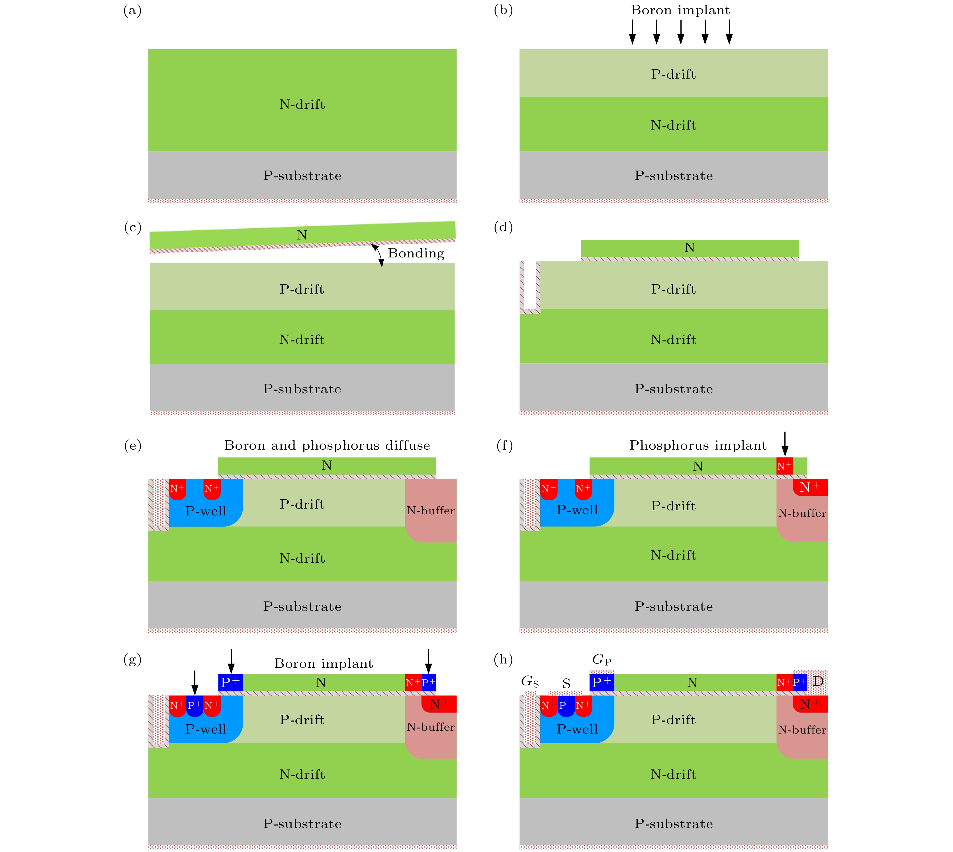
本文提出了一种具有双漂移区和双导通路径的新型横向双扩散金属氧化物半导体(LDMOS)器件, 实现了超低比导通电阻(Ron,sp). 其漂移区采用P型和N型纵向交替所构成的双漂移区结构, 并引入平面栅和槽型栅分别控制P型和N型漂移区, 使得器件能够在漂移区中形成两条独立的电子导通或消失路径. 在对平面栅施加正向电压时, 可使P型漂移区的表面发生反型, 形成连接沟道和N+漏极的高浓度电子反型层, 从而极大提高器件导通时的电子密度, 降低比导通电阻. 槽型栅极的引入可使器件在关断时产生一条额外的电子消失路径, 从而缩短器件的关断时间(toff). 此外, 由于引入P型漂移区, 使得电子在P型漂移区内输运时与其体内的空穴发生复合, 从而加快了电子的消失过程并进一步地缩短器件的toff. 仿真结果表明, 在200 V的击穿电压(BV)等级下, 本文所提出的新型LDMOS的Ron,sp为3.43 mΩ·cm2, 关断时间为9 ns. 相比传统的LDMOS器件, Ron,sp和toff分别下降了90%和11.6%. 该器件不仅实现了Ron,sp和BV的良好折中, 而且缩短了器件的toff, 展现出了优异的器件性能.In order to improve the contradictory between specific on-resistance (Ron,sp) and breakdown voltage (BV) of lateral double-diffused metal oxide semiconductor (LDMOS) and enhance the turn-off characteristic, this paper proposes a novel LDMOS device with dual-drift regions and dual-conduction paths, which achieves an ultra-low Ron,sp. The key feature of the proposed device is the introduction of a dual-drift region structure with alternating P-type and N-type regions, combined with planar and trench gates to control the P-type and N-type drift regions, respectively. This configuration enables the formation of two independent electron conduction paths within the drift region. When a positive voltage is applied to the planar gate, a voltage difference is generated between the surface of the P-type drift region and the body of device’s drift. Therefore, under the influence of the voltage difference, the electrons are pulled to the surface of the P-type drift region to invert and form a high-density electron inversion layer that connects the channel and the N+ drain, significantly increasing the electron density during conduction and reducing the Ron,sp. The introduction of the trench gate provides an additional electron disappearance path, which shortens the device's turn-off time (toff). Furthermore, the introduction of the P-type drift region facilitates the recombination of electrons with holes within the P-type drift region, accelerating the electron disappearance process and further reducing the device’s toff. Furthermore, the proposed device exhibits a more uniform electric field distribution and higher voltage capability is due to the P+N-N+P+ structure adopted in the PolySi-top layer. During the off-state, both the P+N- junctions and the N+P+ junctions generate electric field peaks at the interfaces. These peaks modulate the electric field distribution across the surface of the drift region. Simulation results indicate that at the BV with a level of 200V, the proposed LDMOS exhibits an Ron,sp of 3.43 mΩ·cm² and a toff of 9 ns. Compared with conventional LDMOS devices, the proposed LDMOS possesses a 90% reduction in Ron,sp and an 11.6% decrease in toff. The proposed device not only achieves an excellent trade-off between Ron,sp and BV but also shortens the toff, demonstrating that the device achieves superior performance.
-
Keywords:
- dual-drift /
- dual-conduction paths /
- specific on-resistance /
- breakdown voltage
[1] Kong M, Yi B, Zhang B 2019 IEEE T. Electron. Dev. 66 592
 Google Scholar
[2] Disney D, Chan W, Lam R, Blattner R, Ma S, Seng W, Chen J W, Cornell M, Williams R 2008 20th International Symposium on Power Semiconductor Devices and IC’s Orlando, FL, USA, May 18–22, 2008 pp24–27
[3] Sun W, Shi L, Sun Z, Yi Y, Li H, Lu S 2006 IEEE T. Electron. Dev. 53 891
Google Scholar
[4] Erlbacher T, Bauer A J, Frey L 2010 IEEE Electron Device Lett. 31 464
Google Scholar
[5] Qiao M, Li Y, Zhou X, Li Z, Zhang B 2014 IEEE Electron Device Lett. 35 774
Google Scholar
[6] Baliga B J 2001 Proc. IEEE 89 822
Google Scholar
[7] Efland T R, Tsai C Y, Pendharkar S 1998 International Electron Devices Meeting 1998 San Francisco, CA, USA, December 6–9, 1998 pp679–682
[8] Li M, Chen D, Jung D S, Shi X 2019 2019 China Semiconductor Technology International Conference Shanghai, China, March 17–18, 2019, pp1–3
[9] Baliga B J 2023 Springer Handbook of Semiconductor Devices (Cham: Springer Nature) pp491–523
[10] Baliga B J 2019 Fundamentals of Power Semiconductor Devices (Cham: Springer International Publishing
[11] Appels J A, Vaes H M J 1979 1979 International Electron Devices Meeting December, 1979, pp238–241
[12] Hossain Z 2008 2008 20th International Symposium on Power Semiconductor Devices and IC’s Orlando, FL, USA, May 18–22, 2008 pp133–136
[13] Xiarong H, Bo Z, Xiaorong L, Guoliang Y, Xi C, Zhaoji L 2011 J. Semicond. 32 074006
Google Scholar
[14] Hardikar S, Tadikonda R, Green D W, Vershinin K V, Narayanan E M S 2004 IEEE T. Electron. Dev. 51 2223
Google Scholar
[15] Stengl R, Gosele U 1985 1985 International Electron Devices Washington, DC, USA, December 1–4, 1985 pp154–157
[16] Duan B, Xing L, Wang Y, Yang Y 2022 IEEE T. Electron. Dev. 69 658
Google Scholar
[17] Chen Y, Hu S, Cheng K, Jiang Y, Luo J, Wang J, Tang F, Zhou X, Zhou J, Gan P 2016 Micro. Nanostructures 89 59
[18] Fujihira T 1997 Jpn. J. Appl. Phys. 36 6254
Google Scholar
[19] Chen X B 2000 Chin. J. Electron. 9 6
[20] Baliga B J, Syau T, Venkatraman P 1992 IEEE Electron Device Lett. 13 427
Google Scholar
[21] Wang Y D, Duan B X, Song H T, Yang Y T 2021 IEEE T. Electron. Dev. 68 2414
Google Scholar
[22] Inc. Synopsys 2016 SentaurusTM Device User Guide Verison L-2016.03
[23] Chen W Z, Qin H F, Zhang H S, Han Z S 2022 IEEE T. Electron. Dev. 69 1900
Google Scholar
[24] Zhou K, Luo X R, Li Z J, Zhang B 2015 IEEE T. Electron. Dev. 62 3334
Google Scholar
[25] Cao Z, Sun Q, Zhang H W, Wang Q, Ma C F, Jiao L C 2022 Micromachines 13 843
Google Scholar
[26] Cheng J, Zhang B, Li Z 2008 IEEE Electron Device Lett. 29 645
Google Scholar
[27] Chen Y M, Lee C L, Tsai M H, Lee C T, Wang C C 2018 2018 IEEE 30th International Symposium on Power Semiconductor Devices and ICs Chicago, IL, USA, May 13–17, 2018 pp331–334
[28] Zhang S, Tuan H C, Wu X J, Shi L, Wu J 2016 Microelectron. Reliab. 61 125
Google Scholar
[29] Chen W, Pjencak J, Agam M, Janssens J, Jerome R, Menon S, Griswold M 2021 2021 33rd International Symposium on Power Semiconductor Devices and ICs Nagoya, Japan, May 30–June 03, 2021 pp287–290
[30] Qiao M, Liu W, Yuan L, Xu P, Ma C, Lin F, Liu K, Guo Y, Lin Z, Zhang S, Zhang B 2022 2022 IEEE 34th International Symposium on Power Semiconductor Devices and ICs Vancouver, BC, Canada, May 22–25, 2022 pp149–152
[31] Kong M, Yi B, Chen X 2019 2019 IEEE 13th International Conference on Power Electronics and Drive Systems Toulouse, France, July 09–12, 2019 pp1–4
[32] Fan J, Wang Z G, Zhang B, Luo X R 2013 Chin. Phys. B 22 048501
Google Scholar
[33] Honarkhah S, Nassif-Khalil S, Salama C A T 2004 Proceedings of the 30th European Solid-State Circuits Conference Leuven, Belgium, September 23, 2004 pp117–120
[34] Hölke A, Antoniou M, Udrea F 2020 2020 32nd International Symposium on Power Semiconductor Devices and ICs Vienna, Austria, September 13–18, 2020 pp435–438
-
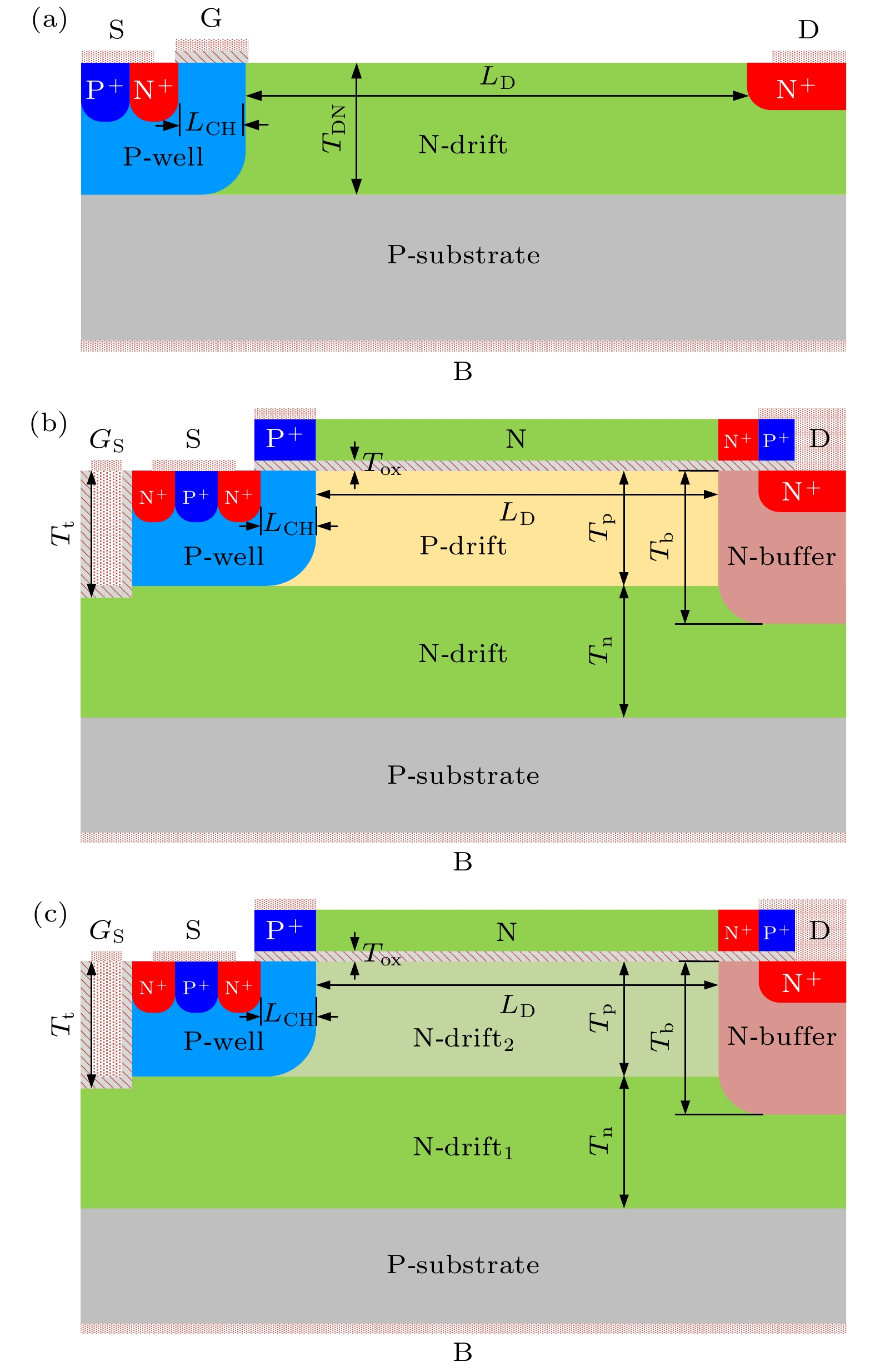
图 1 器件结构图 (a)传统LDMOS; (b) PND-DP LDMOS; (c) NND-DP LDMOS
Fig. 1. Schematic cross-section: (a) Conventional LDMOS; (b) PND-DP LDMOS; (c) NND-DP LDMOS.
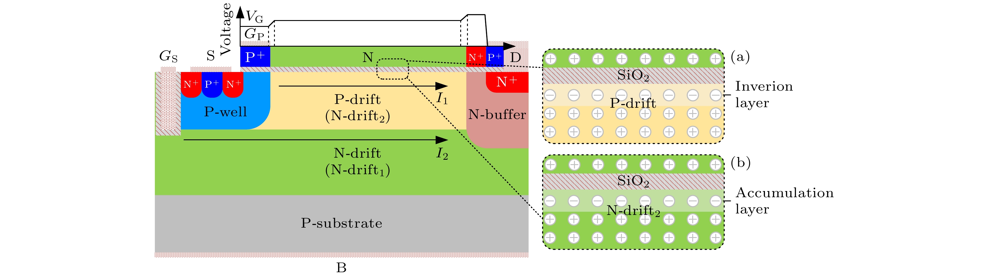
图 2 器件工作原理图 (a) PND-DP LDMOS; (b) NND-DP LDMOS
Fig. 2. Schematic of the proposed devices operation: (a) PND-DP LDMOS; (b) NND-DP LDMOS.
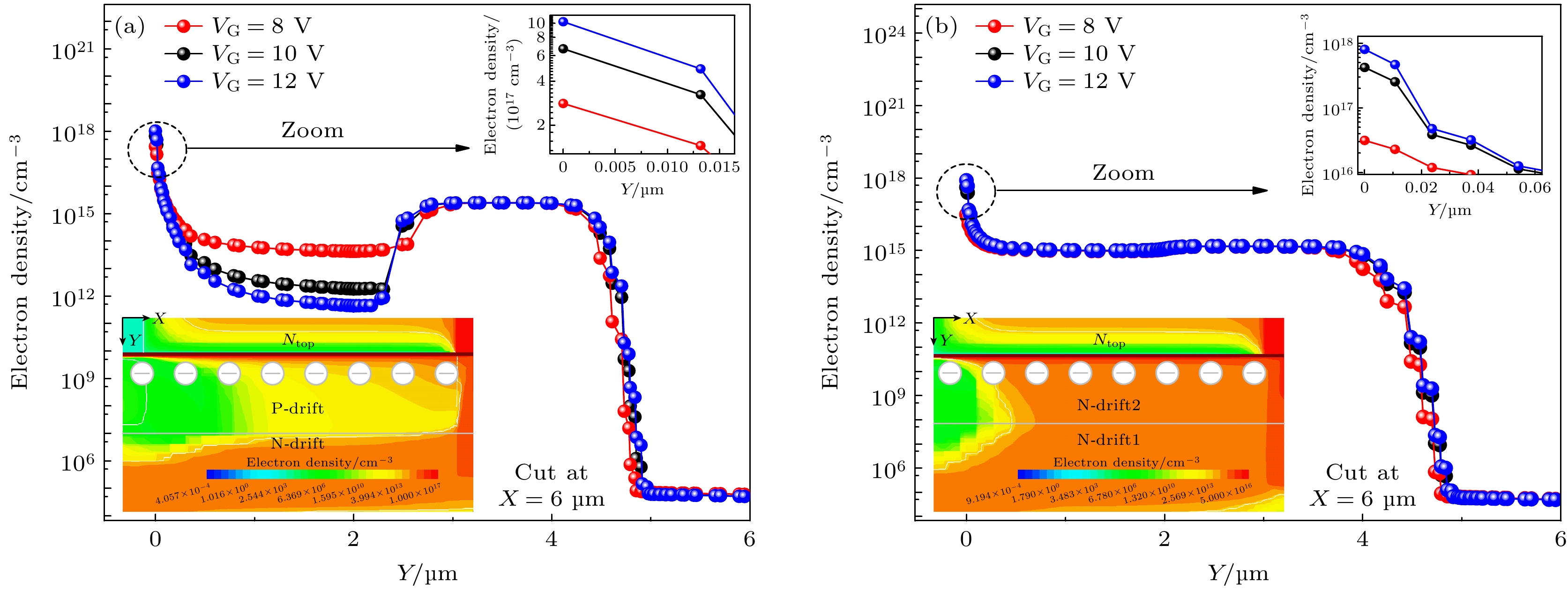
图 5 器件漂移区电子浓度分布曲线 (a) PND-DP LDMOS; (b) NND-DP LDMOS
Fig. 5. Distribution of the drift electron density: (a) PND-DP LDMOS; (b) NND-DP LDMOS.
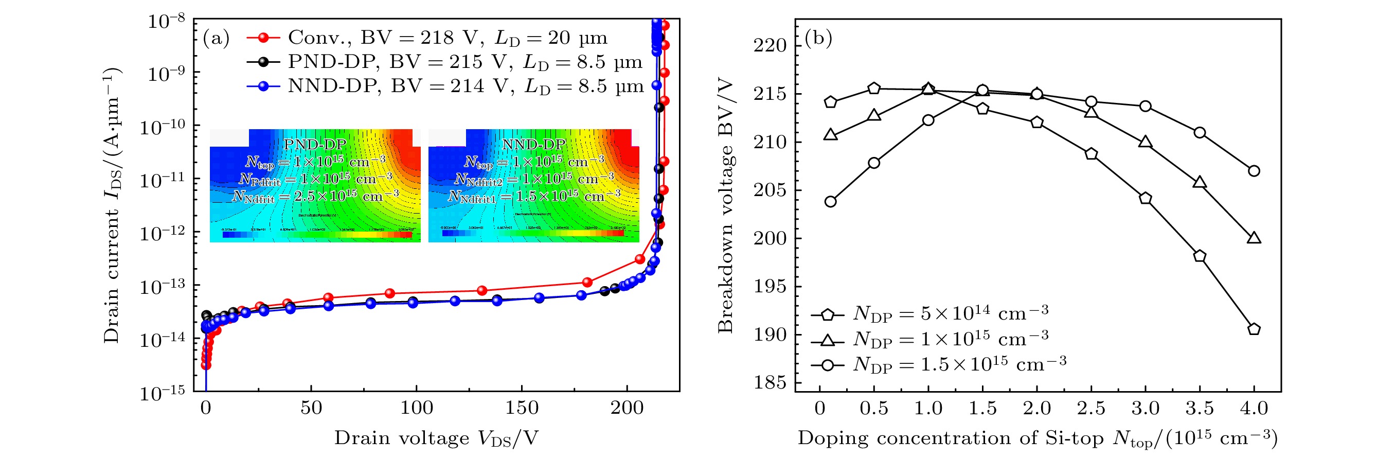
图 6 (a)击穿特性曲线; (b) Ntop对器件击穿特性的影响
Fig. 6. (a) Breakdown characteristic curve; (b) the impact of Ntop on device breakdown characteristics.
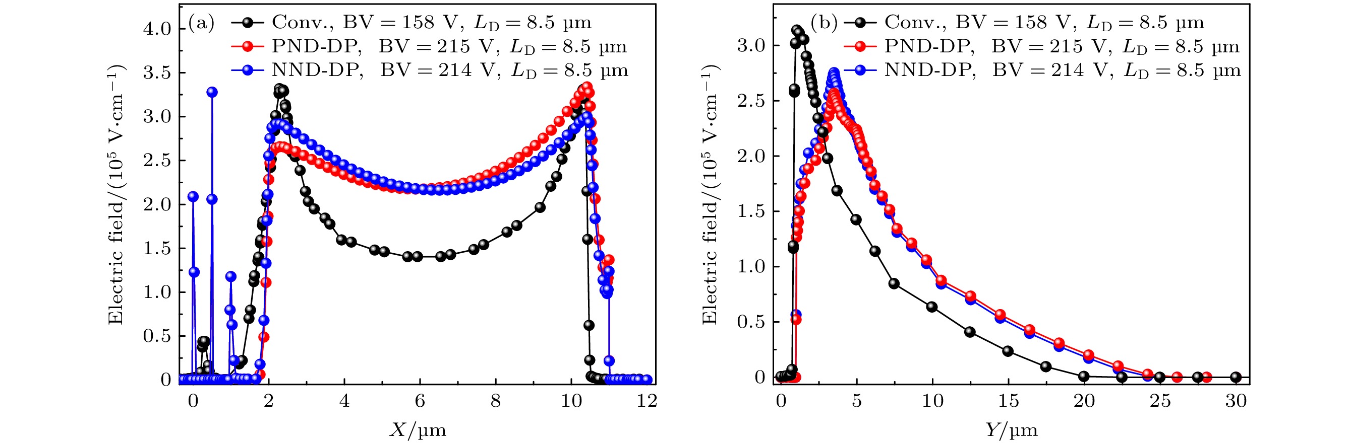
图 7 器件电场分布图 (a) 横向电场; (b)纵向电场
Fig. 7. Device electric field distribution: (a) Lateral electric field; (b) vertical electric field.
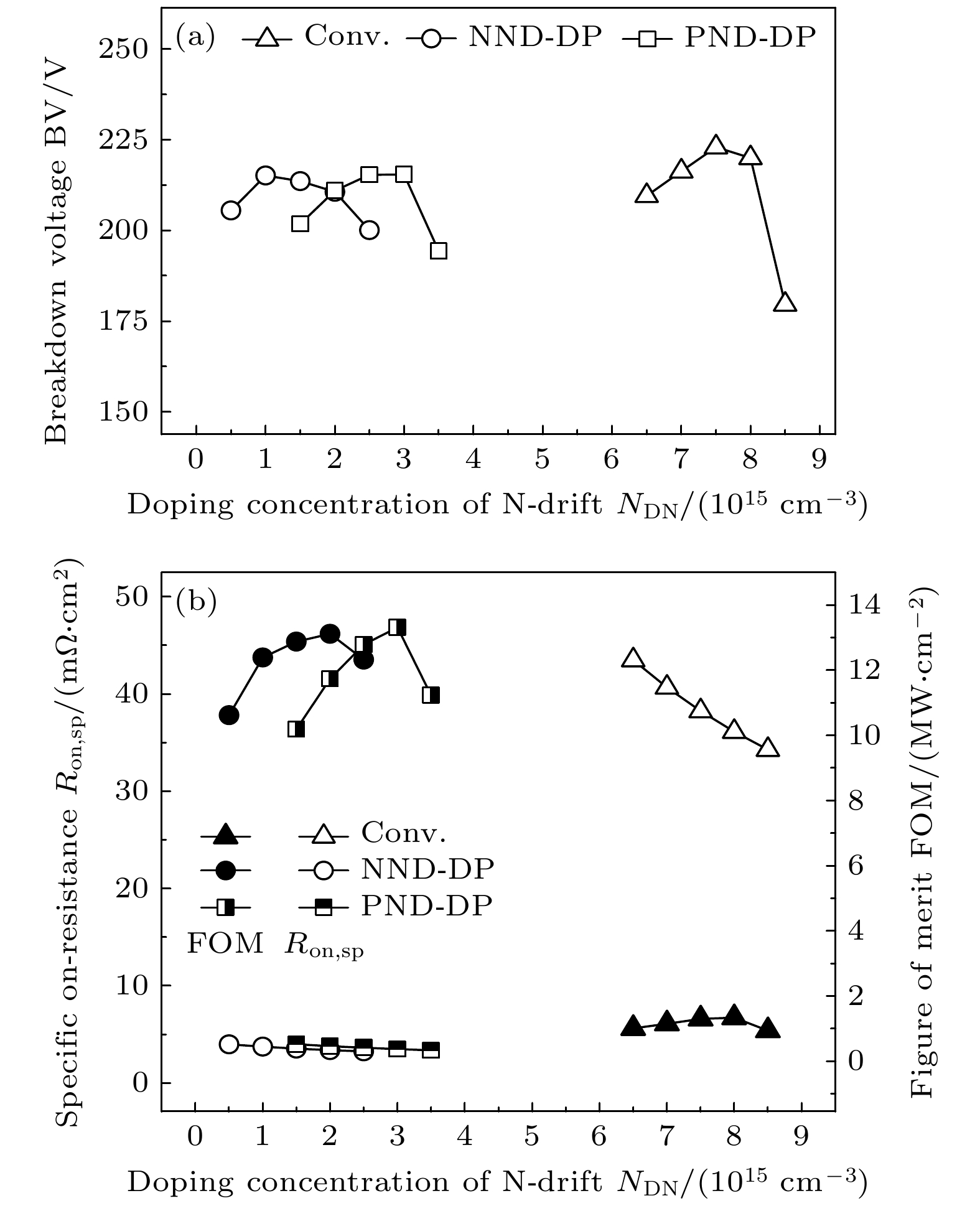
图 8 N-drift 对器件性能的影响 (a) BV; (b) Ron,sp; (c) FOM
Fig. 8. The impact of N-drift on device performance: (a) BV; (b) Ron,sp; (c) FOM.
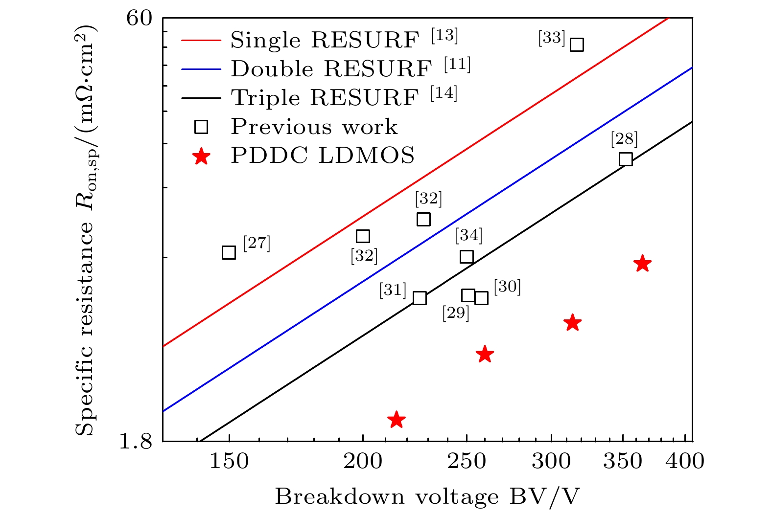
图 9 本文所提出的PND-DP LDMOS与其他器件的Ron,sp-BV比较
Fig. 9. Comparison of Ron,sp-BV between the proposed PND-DP LDMOS and others.
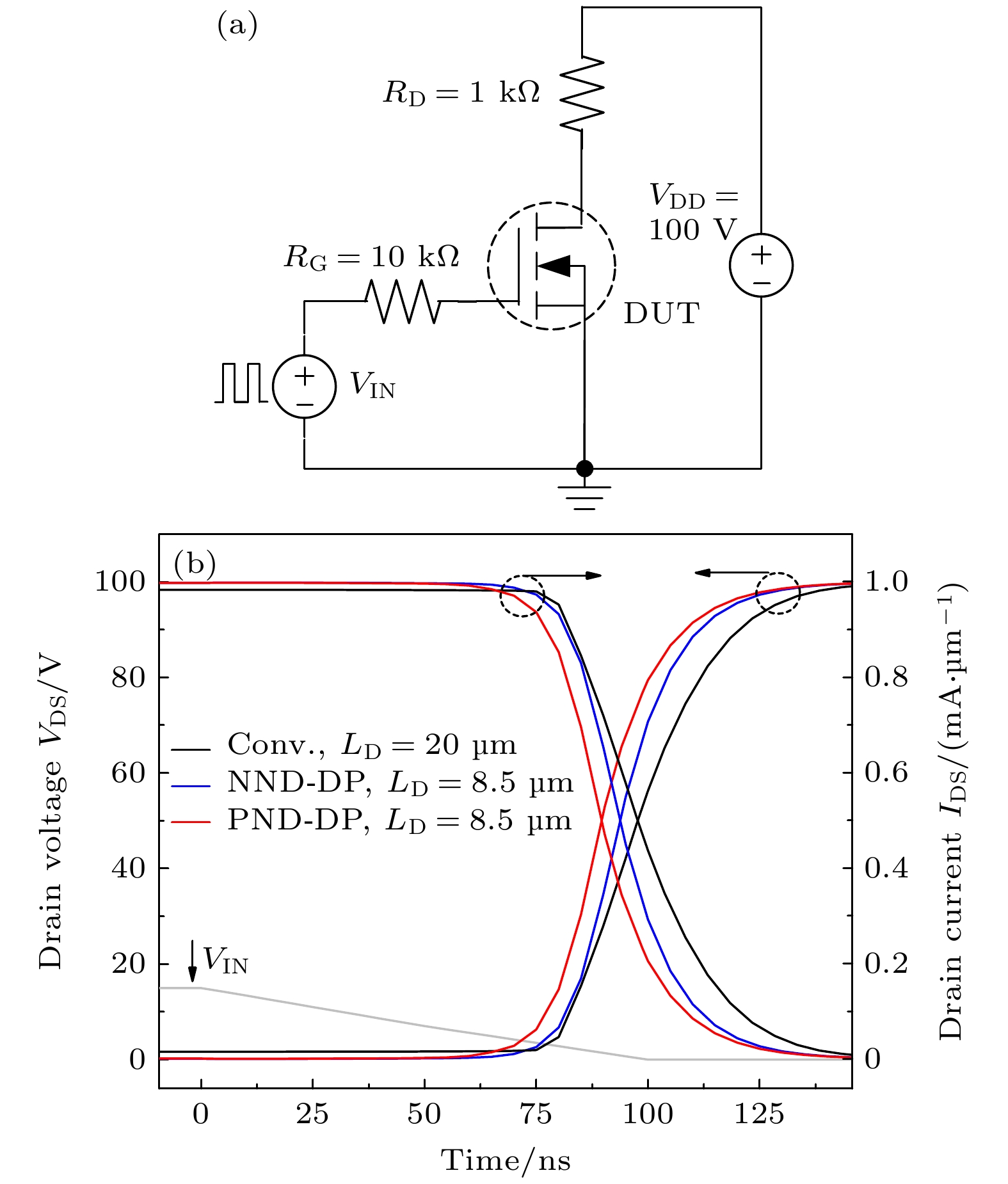
图 10 器件动态特性 (a)测试电路结构; (b)关断特性曲线
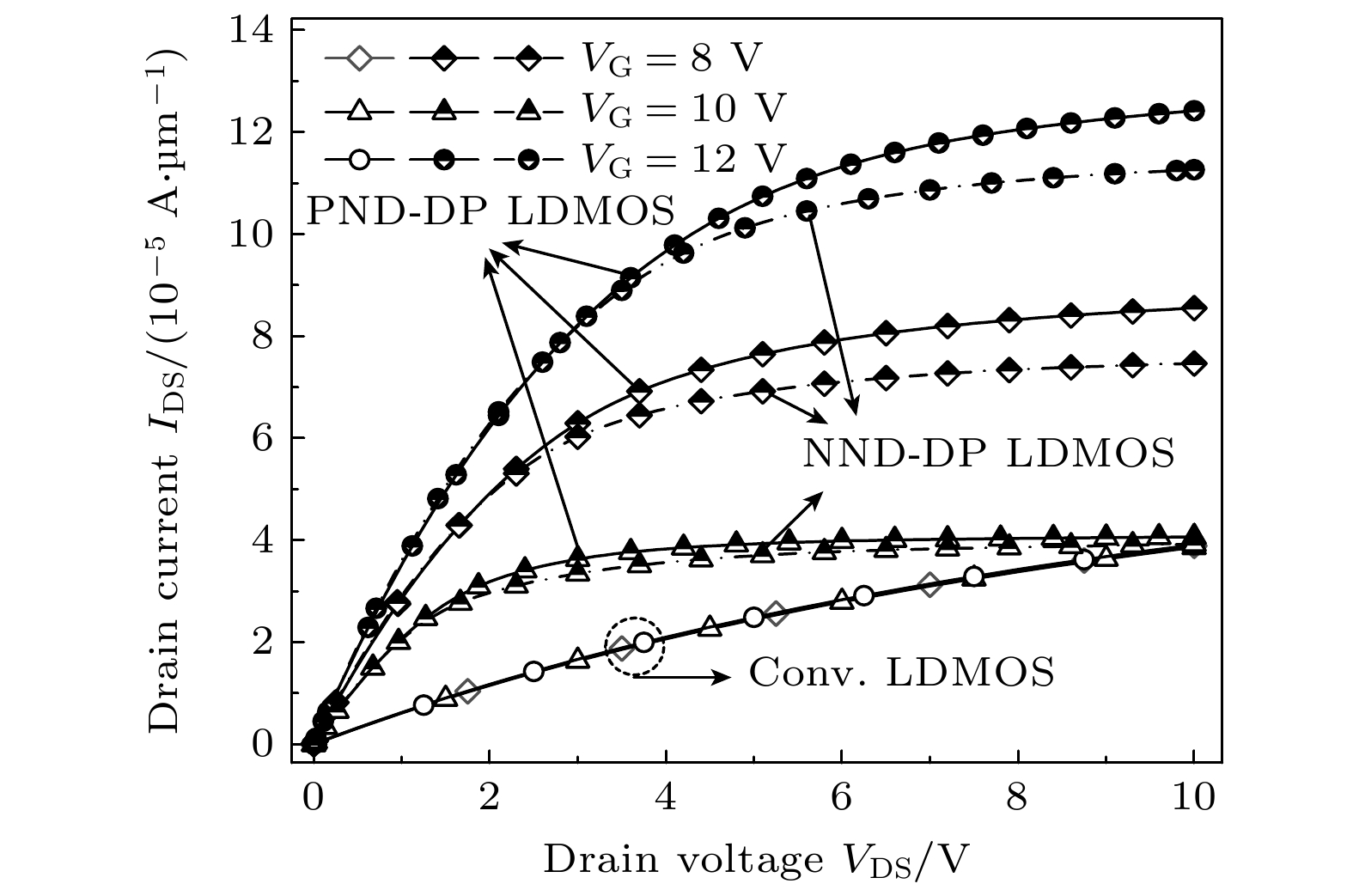
Fig. 10. Device dynamic characteristics: (a) Test circuit structure; (b) turn-off characteristic curve.
表 1 器件仿真中的关键参数
Table 1. Key parameters of devices’ simulation.
参数符号 参数含义 传统 PND-DP NND-DP Tox/μm 氧化层厚度 0.1 0.1 0.1 LD/μm 漂移区长度 20 8.5 8.5 TDP/TDN2/μm P-drift(N-drift2)的厚度 2 2 2 TDN/TDN1/μm N-drift(N-drift1)的厚度 — 3 3 Tb/μm N-buffer的厚度 — 3.5 3.5 LCH/μm 沟道长度 1.5 1.5 1.5 Tt/μm 槽栅的深度 — 2.1 2.1 NDP/NDN2/cm–3 P-drift(N-drift2)的掺杂浓度 — 1×10¹⁵ 1×10¹⁵ NDN/NDN1/cm–3 N-drift(N-drift1) 的掺杂浓度 7.5×10¹⁵ 2.5×10¹⁵ 1.5×10¹⁵ Ntop/cm–3 N-top的掺杂浓度 — 1×10¹⁵ 1×10¹⁵ Nsub/cm–3 衬底的掺杂浓度 3×10¹⁴ 3×10¹⁴ 3×10¹⁴  下载: 导出CSV
表 2 PND-DP LDMOS与其他器件的Ron,sp, BV, FOM
Table 2. Ron,sp, BV, and FOM of PND-DP LDMOS compared with other devices.
下载: 导出CSV
-
[1] Kong M, Yi B, Zhang B 2019 IEEE T. Electron. Dev. 66 592
Google Scholar
[2] Disney D, Chan W, Lam R, Blattner R, Ma S, Seng W, Chen J W, Cornell M, Williams R 2008 20th International Symposium on Power Semiconductor Devices and IC’s Orlando, FL, USA, May 18–22, 2008 pp24–27
[3] Sun W, Shi L, Sun Z, Yi Y, Li H, Lu S 2006 IEEE T. Electron. Dev. 53 891
Google Scholar
[4] Erlbacher T, Bauer A J, Frey L 2010 IEEE Electron Device Lett. 31 464
Google Scholar
[5] Qiao M, Li Y, Zhou X, Li Z, Zhang B 2014 IEEE Electron Device Lett. 35 774
Google Scholar
[6] Baliga B J 2001 Proc. IEEE 89 822
Google Scholar
[7] Efland T R, Tsai C Y, Pendharkar S 1998 International Electron Devices Meeting 1998 San Francisco, CA, USA, December 6–9, 1998 pp679–682
[8] Li M, Chen D, Jung D S, Shi X 2019 2019 China Semiconductor Technology International Conference Shanghai, China, March 17–18, 2019, pp1–3
[9] Baliga B J 2023 Springer Handbook of Semiconductor Devices (Cham: Springer Nature) pp491–523
[10] Baliga B J 2019 Fundamentals of Power Semiconductor Devices (Cham: Springer International Publishing
[11] Appels J A, Vaes H M J 1979 1979 International Electron Devices Meeting December, 1979, pp238–241
[12] Hossain Z 2008 2008 20th International Symposium on Power Semiconductor Devices and IC’s Orlando, FL, USA, May 18–22, 2008 pp133–136
[13] Xiarong H, Bo Z, Xiaorong L, Guoliang Y, Xi C, Zhaoji L 2011 J. Semicond. 32 074006
Google Scholar
[14] Hardikar S, Tadikonda R, Green D W, Vershinin K V, Narayanan E M S 2004 IEEE T. Electron. Dev. 51 2223
Google Scholar
[15] Stengl R, Gosele U 1985 1985 International Electron Devices Washington, DC, USA, December 1–4, 1985 pp154–157
[16] Duan B, Xing L, Wang Y, Yang Y 2022 IEEE T. Electron. Dev. 69 658
Google Scholar
[17] Chen Y, Hu S, Cheng K, Jiang Y, Luo J, Wang J, Tang F, Zhou X, Zhou J, Gan P 2016 Micro. Nanostructures 89 59
[18] Fujihira T 1997 Jpn. J. Appl. Phys. 36 6254
Google Scholar
[19] Chen X B 2000 Chin. J. Electron. 9 6
[20] Baliga B J, Syau T, Venkatraman P 1992 IEEE Electron Device Lett. 13 427
Google Scholar
[21] Wang Y D, Duan B X, Song H T, Yang Y T 2021 IEEE T. Electron. Dev. 68 2414
Google Scholar
[22] Inc. Synopsys 2016 SentaurusTM Device User Guide Verison L-2016.03
[23] Chen W Z, Qin H F, Zhang H S, Han Z S 2022 IEEE T. Electron. Dev. 69 1900
Google Scholar
[24] Zhou K, Luo X R, Li Z J, Zhang B 2015 IEEE T. Electron. Dev. 62 3334
Google Scholar
[25] Cao Z, Sun Q, Zhang H W, Wang Q, Ma C F, Jiao L C 2022 Micromachines 13 843
Google Scholar
[26] Cheng J, Zhang B, Li Z 2008 IEEE Electron Device Lett. 29 645
Google Scholar
[27] Chen Y M, Lee C L, Tsai M H, Lee C T, Wang C C 2018 2018 IEEE 30th International Symposium on Power Semiconductor Devices and ICs Chicago, IL, USA, May 13–17, 2018 pp331–334
[28] Zhang S, Tuan H C, Wu X J, Shi L, Wu J 2016 Microelectron. Reliab. 61 125
Google Scholar
[29] Chen W, Pjencak J, Agam M, Janssens J, Jerome R, Menon S, Griswold M 2021 2021 33rd International Symposium on Power Semiconductor Devices and ICs Nagoya, Japan, May 30–June 03, 2021 pp287–290
[30] Qiao M, Liu W, Yuan L, Xu P, Ma C, Lin F, Liu K, Guo Y, Lin Z, Zhang S, Zhang B 2022 2022 IEEE 34th International Symposium on Power Semiconductor Devices and ICs Vancouver, BC, Canada, May 22–25, 2022 pp149–152
[31] Kong M, Yi B, Chen X 2019 2019 IEEE 13th International Conference on Power Electronics and Drive Systems Toulouse, France, July 09–12, 2019 pp1–4
[32] Fan J, Wang Z G, Zhang B, Luo X R 2013 Chin. Phys. B 22 048501
Google Scholar
[33] Honarkhah S, Nassif-Khalil S, Salama C A T 2004 Proceedings of the 30th European Solid-State Circuits Conference Leuven, Belgium, September 23, 2004 pp117–120
[34] Hölke A, Antoniou M, Udrea F 2020 2020 32nd International Symposium on Power Semiconductor Devices and ICs Vienna, Austria, September 13–18, 2020 pp435–438


 下载:
下载:


计量
- 文章访问数: 2859
- PDF下载量: 69
- 被引次数: 0
