-
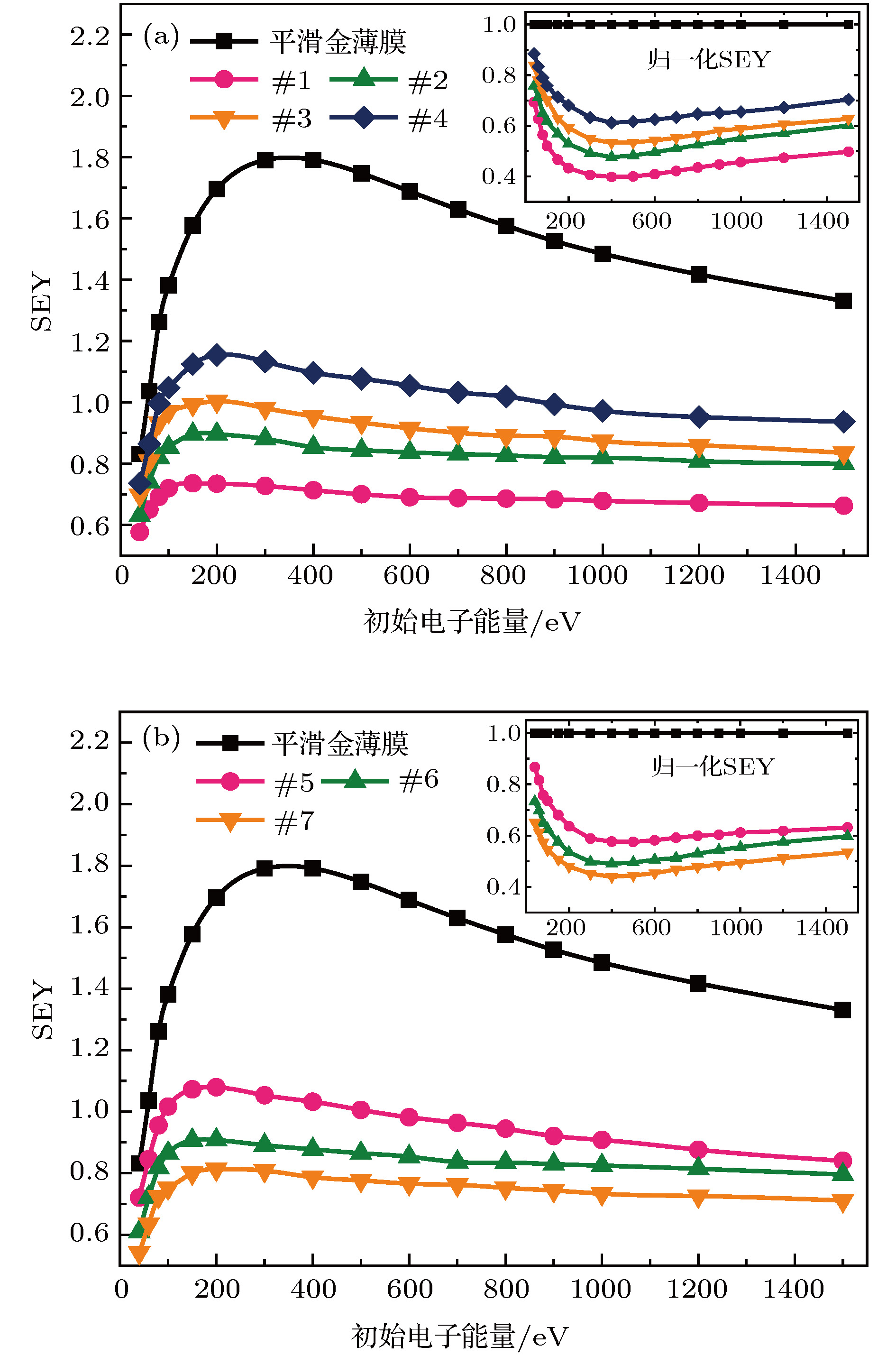
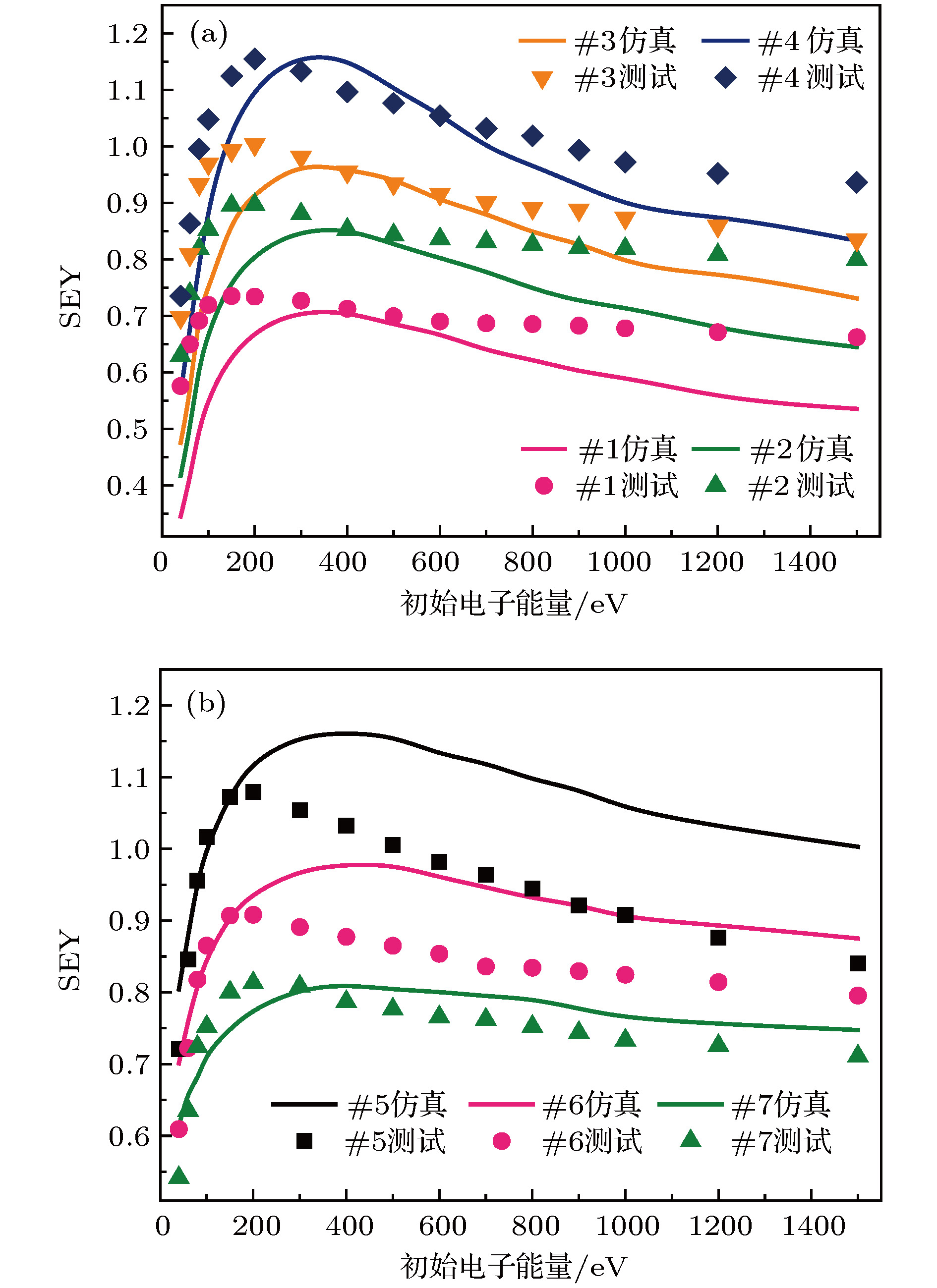
使用红外激光刻蚀技术在镀金铝合金表面制备了多种形貌的微孔及交错沟槽阵列. 表征了两类激光刻蚀微阵列结构的三维形貌和二维精细形貌, 分析了样品表面非理想二级粗糙结构的形成机制. 研究了微阵列结构二次电子发射特性对表面形貌的依赖规律. 实验结果表明: 激光刻蚀得到的微阵列结构能够有效抑制镀金表面二次电子产额(secondary electron yield, SEY), 且抑制能力明显优于诸多其他表面处理技术; 微阵列结构对SEY的抑制能力与其孔隙率及深宽比呈现正相关, 且孔隙率对SEY的影响更为显著. 使用蒙特卡罗模拟方法并结合二次电子发射唯象模型和电子轨迹追踪算法, 仿真了各微结构表面二次电子发射特性, 模拟结果从理论上验证了微阵列结构孔隙率及深宽比对表面SEY的影响规律. 本文获得了能够剧烈降低镀金表面SEY的微阵列结构, 理论分析了SEY对微结构特征参数的依赖规律, 对开发空间微波系统中低SEY表面及提高镀金微波器件性能有重要意义.Multipactor is a frequent discharging phenomenon for space high-power microwave components, and this detrimental effect is mainly induced by secondary electron emission (SEE) and electron resonance in vacuum. Plenty of researches have verified that suppressing SEE is an efficient approach to mitigate the multipactor. Therefore, low SEE yield surfaces are urgently needed for mitigating the multipactor in the field of space science. In the past few decades, a number of technics have been developed to acquire low SEE yield surfaces, including surface coating, surfaces roughening, depositing coessential nanostructure, etc. Laser etching has been partly reported to be an advisable way to construct micro- or nano-structure on some materials’ surfaces, and able to further suppress the SEE yield. Whereas, employing laser etching to obtain the SEE yield reduction on gold coated surfaces is rarely investigated. In this work, by using the laser etching technic, we fabricate four micro hole arrays and three orthogonal groove arrays with various porosities and aspect ratios, and we also characterize their three-dimensional and accurate two-dimensional morphologies. In addition, we investigate the dependence of SEE yield on surface morphology. Experimental results indicate that the laser etched microstructures can effectively suppress the SEE yield from gold coated surfaces, and the suppression levels on SEE yield of these samples are superior to those of many other low SEE yield technics. Furthermore, experiments reveal that the ability to suppress the SEE yield is positively related to the porosity and aspect ratio, as well as that the porosity influences SEE yield more strongly than the aspect ratio does. To theoretically verify the experimental phenomena, we utilize the Monte Carlo method combining with the SEE phenomenological model and the electron trajectory tracking algorithm, to simulate the SEE characteristics of the fabricated microstructures. And the simulation results can qualitatively explain the experimental phenomena. This work digs out an advisable method to sharply reduce the SEE yield from gold coated surfaces by laser etching, which is of considerable importance for exploiting the low SEE yield surface engineering in space microwave systems, and for improving the performance of the space microwave components with gold coated surface.
-
Keywords:
- laser etching /
- microstructure /
- secondary electron emission /
- secondary roughness
[1] Kishek R A, Lau Y Y 1998 Phys. Rev. Lett. 80 3198
 Google Scholar
[2] Vaughan J R M 1988 IEEE Trans. Electron Devices 35 1172
 Google Scholar
[3] Hueso J, Vicente C, Gimeno B, Boria V E, Marini S, Taroncher M 2010 IEEE Trans. Electron Devices 57 3508
 Google Scholar
[4] Nistor V, González L A, Aguilera L, Montero I, Galán L, Wochner U, Raboso D 2014 Appl. Surf. Sci. 315 445
 Google Scholar
[5] Yang J, Cui W Z, Li Y, Xie G B, Zhang N, Wang R, Hu T C, Zhang H T 2016 Appl. Surf. Sci. 382 88
 Google Scholar
[6] Dionne G F 1973 J. Appl. Phys. 44 5361
 Google Scholar
[7] Dionne G F 1975 J. Appl. Phys. 46 3347
 Google Scholar
[8] Cazaux J 2010 Appl. Surf. Sci. 257 1002
 Google Scholar
[9] Ye M, He Y N, Hu S G, Wang R, Hu T C, Yang J, Cui W Z 2013 J. Appl. Phys. 113 074904
 Google Scholar
[10] 叶鸣, 贺永宁, 王瑞 , 胡天存, 张娜, 杨晶, 崔万照, 张忠兵 2014 63 147901
 Google Scholar
Ye M, He Y N, Wang R, Hu T C, Zhang N, Yang J, Cui W Z, Zhang Z B 2014 Acta Phys. Sin. 63 147901
 Google Scholar
[11] Valizadeh R, Malyshev O B, Wang S H, Zolotovskaya S A, Gillespie W A, Abdolvand A 2014 Appl. Phys. Lett. 105 231605
 Google Scholar
[12] Montero I, Mohamed S H, García M, Galán L, Raboso D 2007 J. Appl. Phys. 101 113306
 Google Scholar
[13] Michizono S, Kinbara A, Saito Y, Yamaguchi S, Anami S, Matuda N 1992 J. Vac. Sci. Technol. A 10 1180
 Google Scholar
[14] Wang D, He Y N, Cui W Z 2018 J. Appl. Phys. 124 053301
 Google Scholar
[15] Henrist B, Hilleret N, Scheuerlein C, Taborelli M 2001 Appl. Surf. Sci. 172 95
 Google Scholar
[16] Pimpec F L, Kirby R E, King F, Pivi M 2005 Nucl. Instrum. Methods Phys. Res. A 551 187
 Google Scholar
[17] Luo J, Tian P, Pan C T, Roberson A W, Warner J H, Hill E W, Briggs G A D 2011 ACS Nano 5 1047
 Google Scholar
[18] Thomas S, Pattinson E B 1970 J. Phys. D 3 1469
 Google Scholar
[19] 王丹, 贺永宁, 叶鸣, 崔万照 2018 67 087902
 Google Scholar
Wang D, He Y N, Ye M, Cui W Z 2018 Acta Phys. Sin. 67 087902
 Google Scholar
[20] He Y N, Peng W B, Cui W Z, Ye M, Zhao X L, Wang D, Hu T C, Wang R, Li Y 2016 AIP Adv. 6 025122
 Google Scholar
[21] Valizadeh R, Malyshev O B, Wang S, Sian T, Cropper M D, Sykes N 2017 Appl. Surf. Sci. 404 370
 Google Scholar
[22] 张娜, 曹猛, 崔万照, 张海波 2014 真空科学与技术学报 34 554
Zhang N, Cao M, Cui W Z, Zhang H B 2014 Chinese J. Vac. Sci. Technol. 34 554
[23] Ye M, Wang D, Li Y, He Y N, Cui W Z, Daneshmand M 2017 J. Appl. Phys. 121 074902
 Google Scholar
[24] Wang D, He Y N, Ye M, Peng W B, Cui W Z 2017 J. Appl. Phys. 122 153302
 Google Scholar
[25] Lara J D, Pérez F, Alfonseca M, Galán L, Montero I, Román E, Raboso D, Baquero G 2006 IEEE Trans. Plasma Sci. 34 476
 Google Scholar
-
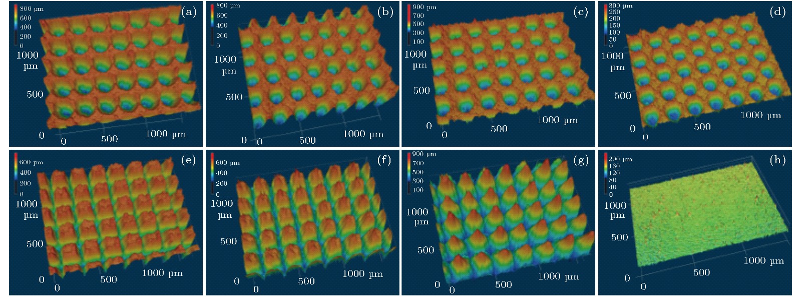
图 2 各镀金铝合金样品的三维形貌 (a) #1样品; (b) #2样品; (c) #3样品; (d) #4样品; (e) #5样品; (f) #6样品; (g) #7样品; (h)未经激光刻蚀处理的平滑镀金表面
Fig. 2. Three-dimensional morphologies of various gold coated samples: (a) Sample #1; (b) sample #2; (c) sample #3; (d) sample #4; (e) sample #5; (f) sample #6; (g) sample #7; (h) untreated flat gold coated surface
表 1 各样品刻蚀单元内图形尺寸及激光刻蚀参数
Table 1. Sizes of the etching patterns and the detailed etching parameters
样品编号 #1 #2 #3 #4 #5 #6 #7 激光功率/W 16 12 10 6 12 12 12 $d/{\text{μ}}\rm{m}$ 150 150 150 150 150 100 50 $b/{\text{μ}}\rm{m}$ 50 50 50 50 50 100 150 $l/{\text{μ}}\rm{m}$ 200 200 200 200 200 200 200 扫描次数 400 100 25 5 250 250 250 理论孔隙率A/% 44.18 44.18 44.18 44.18 43.75 75.00 93.75 表 2 各激光扫描刻蚀样品的特征尺寸、深宽比及孔隙率统计
Table 2. Characteristic sizes, aspect ratio and porosity of the laser etched samples
样品编号 #1 #2 #3 #4 #5 #6 #7 $d/{\text{μ}}\rm{m}$ 165 164 158 155 121 83 34 $h/{\text{μ}}\rm{m}$ 437 324 253 181 306 373 416 深宽比H 2.65 1.98 1.60 1.17 3.87 3.19 2.51 孔隙率A/% 53.46 52.81 49.01 47.17 63.40 82.78 97.11 表 3 三种状态下#4样品表面元素原子比例定量分析
Table 3. Quantitative analysis of atomic proportion under three surface states for sample #4
元素 O Al Ag Au 原始表面 51.64% 8.24% 40.12% 0 激光刻蚀后 15.51% 78.76% 5.73% 0 刻蚀 + 镀金后 11.78% 38.66% 3.92% 45.64% -
[1] Kishek R A, Lau Y Y 1998 Phys. Rev. Lett. 80 3198
 Google Scholar
[2] Vaughan J R M 1988 IEEE Trans. Electron Devices 35 1172
 Google Scholar
[3] Hueso J, Vicente C, Gimeno B, Boria V E, Marini S, Taroncher M 2010 IEEE Trans. Electron Devices 57 3508
 Google Scholar
[4] Nistor V, González L A, Aguilera L, Montero I, Galán L, Wochner U, Raboso D 2014 Appl. Surf. Sci. 315 445
 Google Scholar
[5] Yang J, Cui W Z, Li Y, Xie G B, Zhang N, Wang R, Hu T C, Zhang H T 2016 Appl. Surf. Sci. 382 88
 Google Scholar
[6] Dionne G F 1973 J. Appl. Phys. 44 5361
 Google Scholar
[7] Dionne G F 1975 J. Appl. Phys. 46 3347
 Google Scholar
[8] Cazaux J 2010 Appl. Surf. Sci. 257 1002
 Google Scholar
[9] Ye M, He Y N, Hu S G, Wang R, Hu T C, Yang J, Cui W Z 2013 J. Appl. Phys. 113 074904
 Google Scholar
[10] 叶鸣, 贺永宁, 王瑞 , 胡天存, 张娜, 杨晶, 崔万照, 张忠兵 2014 63 147901
 Google Scholar
Ye M, He Y N, Wang R, Hu T C, Zhang N, Yang J, Cui W Z, Zhang Z B 2014 Acta Phys. Sin. 63 147901
 Google Scholar
[11] Valizadeh R, Malyshev O B, Wang S H, Zolotovskaya S A, Gillespie W A, Abdolvand A 2014 Appl. Phys. Lett. 105 231605
 Google Scholar
[12] Montero I, Mohamed S H, García M, Galán L, Raboso D 2007 J. Appl. Phys. 101 113306
 Google Scholar
[13] Michizono S, Kinbara A, Saito Y, Yamaguchi S, Anami S, Matuda N 1992 J. Vac. Sci. Technol. A 10 1180
 Google Scholar
[14] Wang D, He Y N, Cui W Z 2018 J. Appl. Phys. 124 053301
 Google Scholar
[15] Henrist B, Hilleret N, Scheuerlein C, Taborelli M 2001 Appl. Surf. Sci. 172 95
 Google Scholar
[16] Pimpec F L, Kirby R E, King F, Pivi M 2005 Nucl. Instrum. Methods Phys. Res. A 551 187
 Google Scholar
[17] Luo J, Tian P, Pan C T, Roberson A W, Warner J H, Hill E W, Briggs G A D 2011 ACS Nano 5 1047
 Google Scholar
[18] Thomas S, Pattinson E B 1970 J. Phys. D 3 1469
 Google Scholar
[19] 王丹, 贺永宁, 叶鸣, 崔万照 2018 67 087902
 Google Scholar
Wang D, He Y N, Ye M, Cui W Z 2018 Acta Phys. Sin. 67 087902
 Google Scholar
[20] He Y N, Peng W B, Cui W Z, Ye M, Zhao X L, Wang D, Hu T C, Wang R, Li Y 2016 AIP Adv. 6 025122
 Google Scholar
[21] Valizadeh R, Malyshev O B, Wang S, Sian T, Cropper M D, Sykes N 2017 Appl. Surf. Sci. 404 370
 Google Scholar
[22] 张娜, 曹猛, 崔万照, 张海波 2014 真空科学与技术学报 34 554
Zhang N, Cao M, Cui W Z, Zhang H B 2014 Chinese J. Vac. Sci. Technol. 34 554
[23] Ye M, Wang D, Li Y, He Y N, Cui W Z, Daneshmand M 2017 J. Appl. Phys. 121 074902
 Google Scholar
[24] Wang D, He Y N, Ye M, Peng W B, Cui W Z 2017 J. Appl. Phys. 122 153302
 Google Scholar
[25] Lara J D, Pérez F, Alfonseca M, Galán L, Montero I, Román E, Raboso D, Baquero G 2006 IEEE Trans. Plasma Sci. 34 476
 Google Scholar
计量
- 文章访问数: 10563
- PDF下载量: 77
- 被引次数: 0


 下载:
下载:


