-
Titanium monoxide has attracted great attention due to its unique superconducting characteristics and potential applications in microelectronics. In this work, a series of TiO thin films are prepared at room temperature by using the radio frequency magnetron sputtering method through changing the oxygen partial pressures. The crystal structures, valences of the elements, and electrical transport properties of the films are investigated systematically. X-ray diffraction results indicate that the films are epitaxially grown on MgO single crystal substrates along the [001] direction. After the surface of the TiO film is treated by ion etching, it is found that the Ti element mainly exists in a divalent form. For all films, the temperature coefficients of resistance are negative above superconducting transition temperature Tc. The films prepared under high oxygen partial pressures reveal insulator characteristics, and the temperature dependence of resistivity obeys the Mott-type variable-range-hopping law in low temperature regime. The films prepared under low oxygen partial pressures exhibit metallic properties, and enter into a superconducting state at low temperature. The superconducting transition temperature Tc in our film can be as high as 3.05 K. The carrier concentrations of the films are in the vicinity of ~2.0×1022 cm–3, which is comparable to those for the typical metals. Interestingly, it is found that the main species of the charge carriers in the films transforms from electrons to holes with the oxygen partial pressure decreasing. The crossover of the species of the charge carriers could related to the changing of energy-band structure with the oxygen content in TiO film.
-
Keywords:
- titanium oxide thin films /
- magnetron sputtering /
- electrical transport properties /
- superconductivity
[1] Reed T B, Banus M D, Sjöstrand M, Keesom P H 1972 J. Appl. Phys. 43 2478
 Google Scholar
[2] Valeeva A A, Rempel A A, Gusev A I 2001 JETP Lett. 73 621
 Google Scholar
[3] Doyle N J, Hulm J K, Jones C K, Miller R C, Taylor A 1968 Phys. Lett. A 26 604
[4] Banus M D, Reed T B, Strauss A J 1972 Phys. Rev. B 5 2775
 Google Scholar
[5] Hulm J K, Jones C K, Hein R A, Gibson J W 1972 J. Low Temp. Phys. 7 291
 Google Scholar
[6] Zhang C, Hao F X, Gao G Y, Liu X, Ma C, Lin Y, Yin Y W, Li X G 2017 npj Quantum Mater. 2 2
 Google Scholar
[7] Liu X, Zhang C, Hao F X, Wang T Y, Fan Y J, Yin Y W, Li X G 2017 Phys. Rev. B 96 104505
 Google Scholar
[8] Fan Y J, Ma C, Wang T Y, Zhang C, Chen Q L, Liu X, Wang Z Q, Li Q, Yin Y W, Li X G 2018 Phys. Rev. B 98 064501
 Google Scholar
[9] Fan Y J, Zhang C, Liu X, Lin Y, Gao G Y, Ma C, Yin Y W, Li X G 2019 J. Alloys Compd. 786 607
 Google Scholar
[10] Wang D, Huang C, He J Q, Che X L, Zhang H, Huang F Q 2017 ACS Omega 2 1036
 Google Scholar
[11] Xu J, Wang D, Yao H, Bu K, Pan J, He J Q, Xu F, Hong Z, Chen X, Huang F Q 2018 Adv. Mater. 30 1706240
 Google Scholar
[12] Li F, Zou Y, Han M G, Foyevtsova K, Shin H, Lee S, Liu C, Shin K, Albright S D, Sutarto R, He F, Davidson B A, Walker F J, Ahn C H, Zhu Y, Cheng Z G, Elfimov I, Sawatzky G A, Zou K 2021 Sci. Adv. 7 eabd4248
 Google Scholar
[13] Zhang C, Fan Y J, Chen Q, Wang T Y, Liu X, Li Q, Yin Y W, Li X G 2019 NPG Asia Mater. 11 76
 Google Scholar
[14] Zhang C, Hao F X, Liu X, Fan Y J, Wang T Y, Yin Y W, Li X G 2018 Supercond. Sci. Technol. 31 015016
 Google Scholar
[15] Grigorov K G, Grigorov G I, Drajeva L, Bouchier D, Sporkend R, Caudano R 1998 Vacuum 51 153
 Google Scholar
[16] Banakh O, Schmid P E, Sanjines R, Levy F 2002 Surf. Coat. Technol. 151 272
[17] Bulyarskiy S V, Koiva D A, Belov V S, Zenova E V, Rudakov G А, Gusarov G G 2021 J. Vac. Sci. Technol. A 39 053403
 Google Scholar
[18] Jeong D S, Thomas R, Katiyar R S, Scott J F, Kohlstedt H, Petraru A, Hwang C S 2012 Rep. Prog. Phys. 75 076502
 Google Scholar
[19] Yang J, Strukov D, Stewart D 2013 Nat. Nanotechnol. 8 13
 Google Scholar
[20] Assim E M 2008 J. Alloys Compd. 465 1
 Google Scholar
[21] Nguyen T T N, Chen Y H, He J L 2014 Thin Solid Films 572 8
 Google Scholar
[22] Okinaka N, Akiyama T 2006 Jpn. J. Appl. Phys. 45 7009
 Google Scholar
[23] He Q, Hao Q, Chen G, Poudel B, Wang X, Wang D, Ren Z 2007 Appl. Phys. Lett. 91 052505
 Google Scholar
[24] Okinaka N, Akiyama T 2010 ISIJ Int. 50 1296
 Google Scholar
[25] Shklovskii B I, Efros A L 1984 Electronic Properties of Doped Semiconductors (Berlin: Springer) pp180–222
[26] Gantmakher V F 2005 Electrons and Disorder in Solids (Oxford: Clarendon) pp58–73
[27] Kuznetsov M V, Zhuravlev J F, Zhilyaev V A, Gubanov V A 1992 J. Electron Spectrosc. Relat. Phenomena 58 1
 Google Scholar
[28] Netterfield R P, Martin P J, Pacey C G, Sainty W G, McKenzie D R, Auchterlonie G 1989 J. Appl. Phys. 66 1805
 Google Scholar
[29] Möbius A 1989 Phys. Rev. B 40 4194
 Google Scholar
[30] Sachser R, Porrati F, Schwalb C H, Huth M 2011 Phys. Rev. Lett. 107 206803
 Google Scholar
[31] Kittel C 2005 Introduction to Solid State Physics (Hoboken: John Wiley) p155
[32] Foner S 1957 Phys. Rev. 107 1513
 Google Scholar
[33] Berlincourt T G 1959 Phys. Rev. 114 969
 Google Scholar
[34] Scovil G W 1966 Appl. Phys. Lett. 9 247
 Google Scholar
[35] Huang Y L, Chiu S P, Zhu Z X, Li Z Q, Lin J J 2010 J. Appl. Phys. 107 063715
 Google Scholar
-
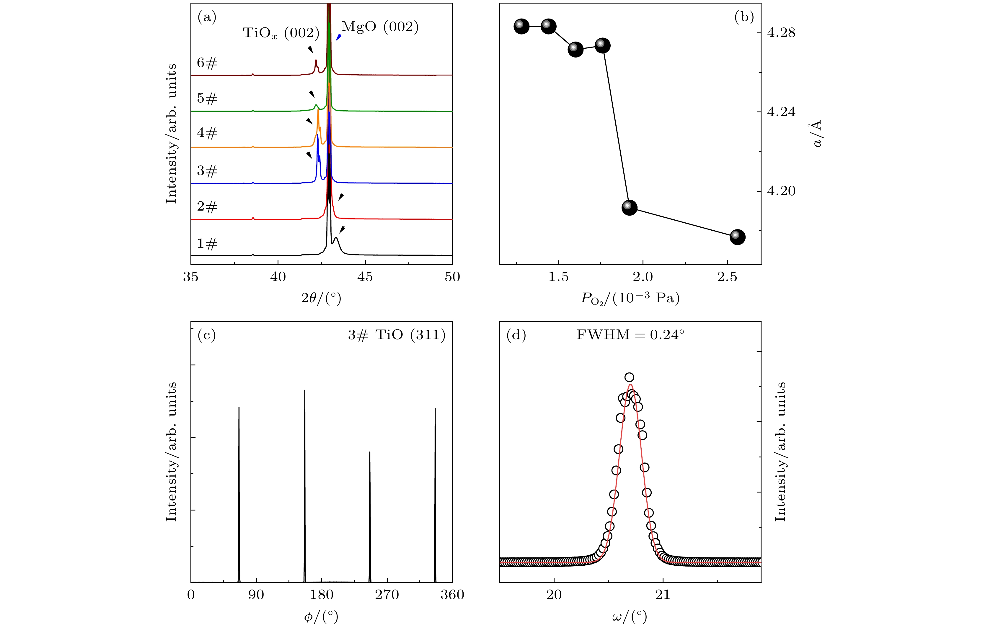
图 1 不同氧分压下制备的TiO薄膜样品的XRD测量结果 (a) θ-2θ图谱; (b) 晶格常数与氧分压的关系; (c) 代表性样品3# (311)晶面的φ扫描图谱; (d) 代表性样品3# (002)晶面的ω扫描图谱, 实线为高斯拟合结果
Figure 1. XRD results for TiO thin films prepared under different oxygen partial pressures: (a) θ-2θ pattern; (b) relationship between lattice constant and oxygen partial pressure; (c) φ scan pattern of the representative sample 3# along (311) crystal face; (d) ω scan pattern of the representative sample 3# along (002) crystal face, the solid curve is the Gaussian fitting result.
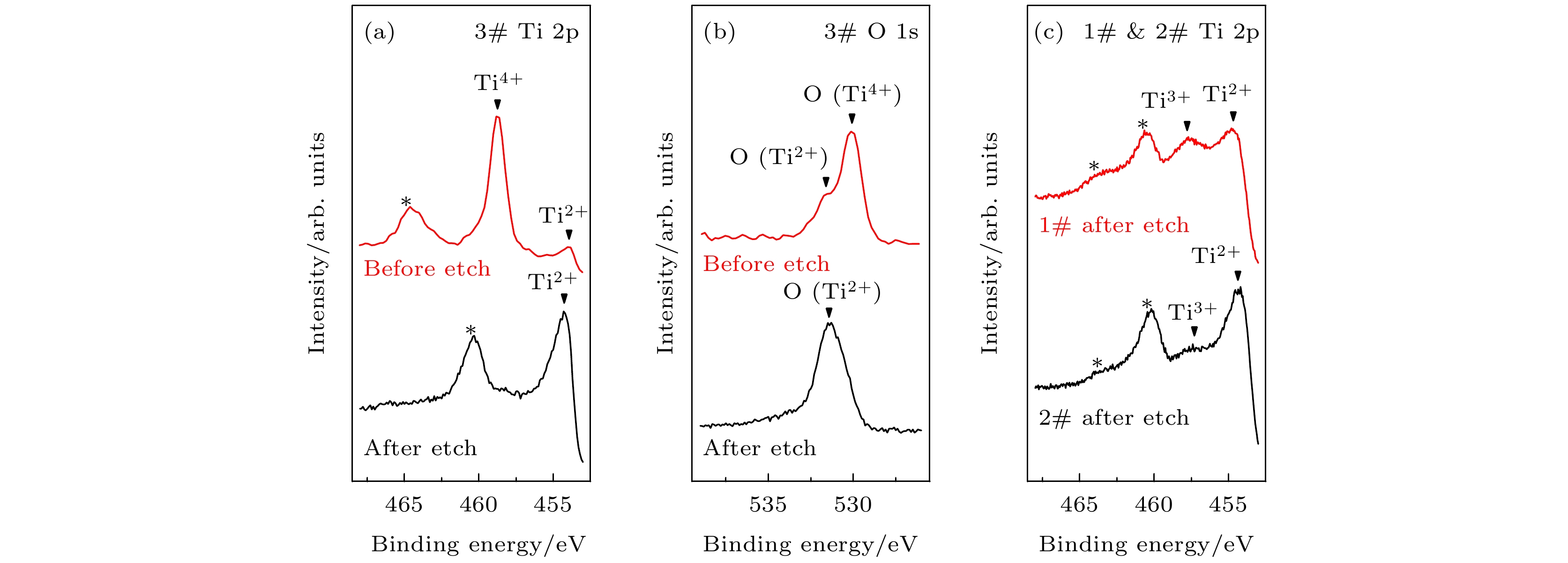
图 2 TiO薄膜的XPS图谱 (a), (b) 代表性样品3# (低氧分压下制备的样品) 氩离子刻蚀前后Ti 2p轨道和O 1s轨道的精细图谱; (c) 样品1#和2#刻蚀后Ti 2p轨道的精细图谱, 图中倒三角型符号标注了Ti 2p3/2峰的位置, Ti 2p1/2峰的位置用*标注
Figure 2. XPS spectra of TiO thin films: (a), (b) Spectra of Ti 2p and O 1s orbitals for the representative sample 3# (prepared under low oxygen partial pressure) before and after argon ion etching; (c) XPS spectra of Ti 2p orbitals of samples 1# and 2# after etching, the position of Ti 2p3/2 peak is marked by the inverted triangle symbol and the position of Ti 2p1/2 peak is marked with *
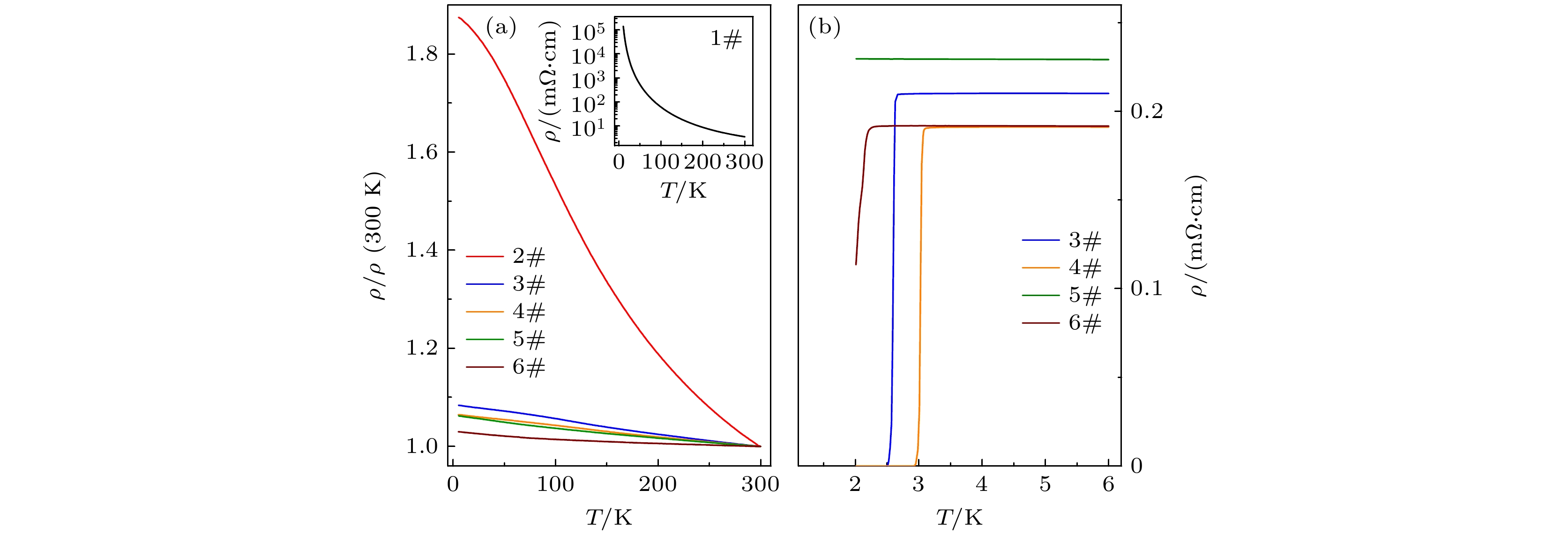
图 3 (a) TiO薄膜样品的归一化电阻率ρ/ρ(300 K)与温度T的关系, 插图为1#样品电阻率ρ随温度的变化关系; (b) 6 K以下样品3#—6#的电阻率随温度的变化关系
Figure 3. (a) Normalized resistivity ρ/ρ(300 K) of TiO thin films as a function of temperature T, the inset shows the relationship between resistivity ρ and temperature for sample 1#; (b) relationship between the resistivity and temperature of samples 3#–6# below 6 K.
图 5 250 K下TiO薄膜的Hall测量结果 (a) 横向电阻
${R_{xy}}$ 随磁场${\mu _0}H$ 的变化; (b)样品的霍尔系数${R_{\text{H}}}$ 和载流子浓度n与氧分压的关系Figure 5. Hall measurement results of TiO thin films at 250 K: (a) Change in transverse resistance
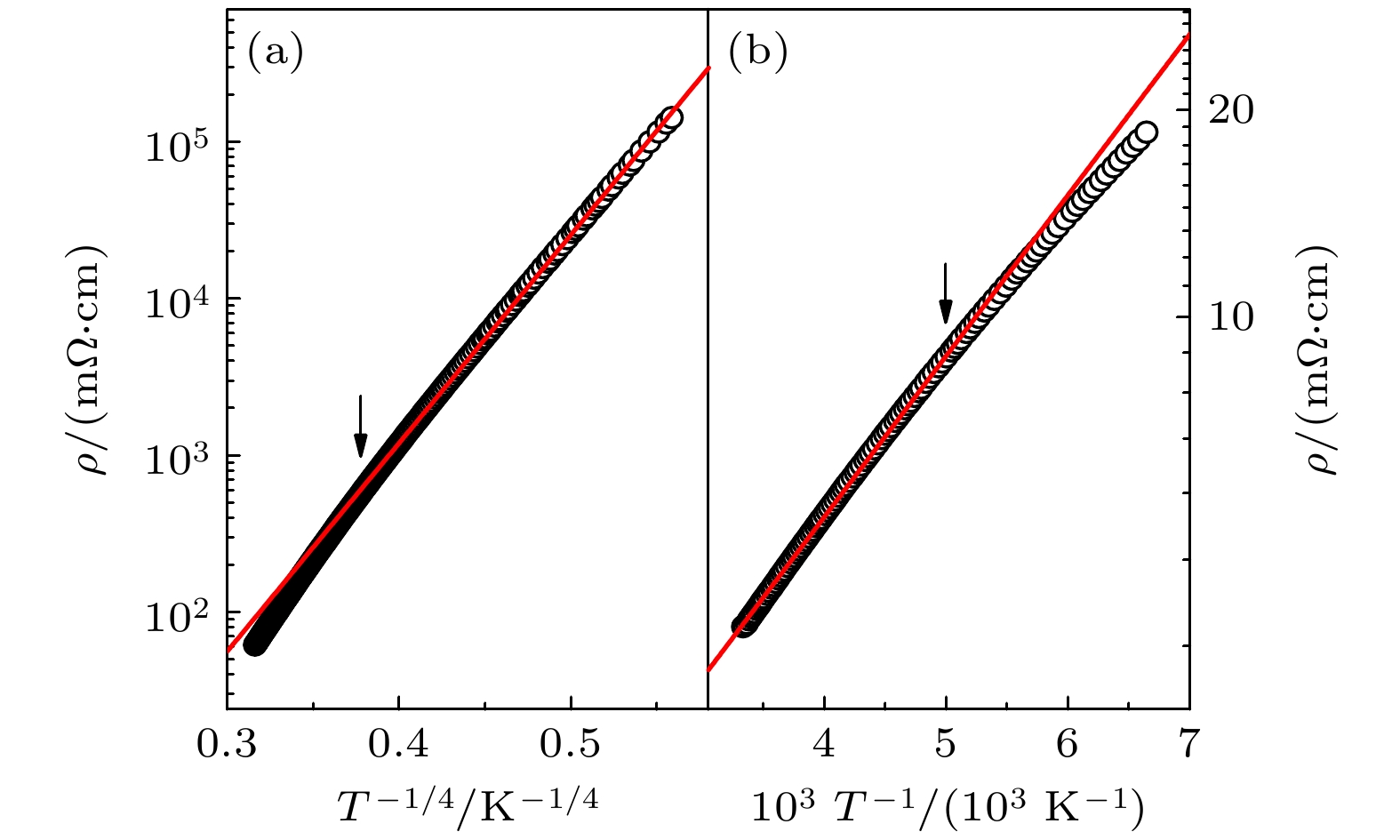
${R_{xy}}$ as a function of magnetic field${\mu _0}H$ ; (b) relationship between Hall coefficient${R_{\text{H}}}$ and carrier concentration n of samples and oxygen partial pressure.图 6 (a) 10—100 K下, 样品1#的lnρ与
${T^{ - 1/4}}$ 的关系图, 实线为(1)式的最小二乘拟合结果; (b) 150—300 K下, 样品1#的lnρ与1000/T的关系图, 实线为(3)式的最小二乘拟合结果Figure 6. (a) Relationship between lnρ and
${T^{ - 1/4}}$ for sample 1# from 10 K to 100 K, with the solid line representing the least-squares fit of Eq. (1); (b) relationship between lnρ and 1000/T for sample 1# from 150 K to 300 K, with the solid line representing the least-squares fit of Eq. (3).表 1 TiO薄膜的基本参数, 其中t为薄膜平均厚度,
$ {P_{{{\text{O}}_2}}} $ 为样品生长时的氧分压, a为晶格常数, ρ(300 K) 和ρ(5 K) 分别为300 K和5 K温度下样品的电阻率,${T_{\text{c}}}$ 为超导样品的超导转变温度,${R_{\text{H}}}$ 和n分别为250 K下测得的霍尔系数和载流子浓度Table 1. Basic parameters of TiO thin films, where t is the average thickness of the thin film,
$ {P_{{{\text{O}}_2}}} $ is the oxygen partial pressure during sample growth, a is the lattice constant, ρ(300 K) and ρ(5 K) are the resistivities of the sample at 300 K and 5 K,${T_{\text{c}}}$ is the superconducting critical temperature of the superconducting sample,${R_{\text{H}}}$ and n are the Hall coefficient and carrier concentration measured at 250 K, respectively.样品 t/nm $ {P_{{{\text{O}}_2}}} $
/(10–3 Pa)a/Å ρ(300 K)
/(mΩ·cm)ρ(5 K)
/(mΩ·cm)${T_{\text{c}}}$/K ${R_{\text{H}}}$
/(10–10 m3·C–1)n
/(1022 cm–3)1# 453.85 2.56 4.179 3.557 — — –2.610 2.380 2# 400.05 1.92 4.192 0.322 0.603 — –0.654 9.494 3# 350.45 1.76 4.274 0.194 0.210 2.61 0.309 20.074 4# 302.70 1.60 4.272 0.180 0.191 3.05 0.564 11.004 5# 286.25 1.44 4.283 0.216 0.229 — 1.865 3.330 6# 292.10 1.28 4.283 0.186 0.192 2.13 1.311 4.738 -
[1] Reed T B, Banus M D, Sjöstrand M, Keesom P H 1972 J. Appl. Phys. 43 2478
 Google Scholar
[2] Valeeva A A, Rempel A A, Gusev A I 2001 JETP Lett. 73 621
 Google Scholar
[3] Doyle N J, Hulm J K, Jones C K, Miller R C, Taylor A 1968 Phys. Lett. A 26 604
[4] Banus M D, Reed T B, Strauss A J 1972 Phys. Rev. B 5 2775
 Google Scholar
[5] Hulm J K, Jones C K, Hein R A, Gibson J W 1972 J. Low Temp. Phys. 7 291
 Google Scholar
[6] Zhang C, Hao F X, Gao G Y, Liu X, Ma C, Lin Y, Yin Y W, Li X G 2017 npj Quantum Mater. 2 2
 Google Scholar
[7] Liu X, Zhang C, Hao F X, Wang T Y, Fan Y J, Yin Y W, Li X G 2017 Phys. Rev. B 96 104505
 Google Scholar
[8] Fan Y J, Ma C, Wang T Y, Zhang C, Chen Q L, Liu X, Wang Z Q, Li Q, Yin Y W, Li X G 2018 Phys. Rev. B 98 064501
 Google Scholar
[9] Fan Y J, Zhang C, Liu X, Lin Y, Gao G Y, Ma C, Yin Y W, Li X G 2019 J. Alloys Compd. 786 607
 Google Scholar
[10] Wang D, Huang C, He J Q, Che X L, Zhang H, Huang F Q 2017 ACS Omega 2 1036
 Google Scholar
[11] Xu J, Wang D, Yao H, Bu K, Pan J, He J Q, Xu F, Hong Z, Chen X, Huang F Q 2018 Adv. Mater. 30 1706240
 Google Scholar
[12] Li F, Zou Y, Han M G, Foyevtsova K, Shin H, Lee S, Liu C, Shin K, Albright S D, Sutarto R, He F, Davidson B A, Walker F J, Ahn C H, Zhu Y, Cheng Z G, Elfimov I, Sawatzky G A, Zou K 2021 Sci. Adv. 7 eabd4248
 Google Scholar
[13] Zhang C, Fan Y J, Chen Q, Wang T Y, Liu X, Li Q, Yin Y W, Li X G 2019 NPG Asia Mater. 11 76
 Google Scholar
[14] Zhang C, Hao F X, Liu X, Fan Y J, Wang T Y, Yin Y W, Li X G 2018 Supercond. Sci. Technol. 31 015016
 Google Scholar
[15] Grigorov K G, Grigorov G I, Drajeva L, Bouchier D, Sporkend R, Caudano R 1998 Vacuum 51 153
 Google Scholar
[16] Banakh O, Schmid P E, Sanjines R, Levy F 2002 Surf. Coat. Technol. 151 272
[17] Bulyarskiy S V, Koiva D A, Belov V S, Zenova E V, Rudakov G А, Gusarov G G 2021 J. Vac. Sci. Technol. A 39 053403
 Google Scholar
[18] Jeong D S, Thomas R, Katiyar R S, Scott J F, Kohlstedt H, Petraru A, Hwang C S 2012 Rep. Prog. Phys. 75 076502
 Google Scholar
[19] Yang J, Strukov D, Stewart D 2013 Nat. Nanotechnol. 8 13
 Google Scholar
[20] Assim E M 2008 J. Alloys Compd. 465 1
 Google Scholar
[21] Nguyen T T N, Chen Y H, He J L 2014 Thin Solid Films 572 8
 Google Scholar
[22] Okinaka N, Akiyama T 2006 Jpn. J. Appl. Phys. 45 7009
 Google Scholar
[23] He Q, Hao Q, Chen G, Poudel B, Wang X, Wang D, Ren Z 2007 Appl. Phys. Lett. 91 052505
 Google Scholar
[24] Okinaka N, Akiyama T 2010 ISIJ Int. 50 1296
 Google Scholar
[25] Shklovskii B I, Efros A L 1984 Electronic Properties of Doped Semiconductors (Berlin: Springer) pp180–222
[26] Gantmakher V F 2005 Electrons and Disorder in Solids (Oxford: Clarendon) pp58–73
[27] Kuznetsov M V, Zhuravlev J F, Zhilyaev V A, Gubanov V A 1992 J. Electron Spectrosc. Relat. Phenomena 58 1
 Google Scholar
[28] Netterfield R P, Martin P J, Pacey C G, Sainty W G, McKenzie D R, Auchterlonie G 1989 J. Appl. Phys. 66 1805
 Google Scholar
[29] Möbius A 1989 Phys. Rev. B 40 4194
 Google Scholar
[30] Sachser R, Porrati F, Schwalb C H, Huth M 2011 Phys. Rev. Lett. 107 206803
 Google Scholar
[31] Kittel C 2005 Introduction to Solid State Physics (Hoboken: John Wiley) p155
[32] Foner S 1957 Phys. Rev. 107 1513
 Google Scholar
[33] Berlincourt T G 1959 Phys. Rev. 114 969
 Google Scholar
[34] Scovil G W 1966 Appl. Phys. Lett. 9 247
 Google Scholar
[35] Huang Y L, Chiu S P, Zhu Z X, Li Z Q, Lin J J 2010 J. Appl. Phys. 107 063715
 Google Scholar
Catalog
Metrics
- Abstract views: 4270
- PDF Downloads: 91
- Cited By: 0


 DownLoad:
