-
All-dielectric metamaterial broadband reflectors have the advantages of low loss, high reflection efficiency, and compact structure. An in-depth understanding of the formation mechanism of their reflection bands is of great significance in optimizing metamaterial structure and performance, and in further designing novel photonic devices as well. In this work, two all-dielectric metamaterial broadband reflectors are constructed by using discrete silicon nanopillar array and silicon nanopillar array connected with a silicon sublayer. The quasi-normal modes of the metamaterial reflectors are solved. Combining the quasi-normal modes with the scattering matrix theory, we obtain the fitted reflection spectra of the metamaterial, and then reveal that the zero-frequency quasi-normal mode has a substantial influence on the accuracy of the fitting results. A dispersion relation analysis method is proposed to accurately solve the zero-frequency quasi-normal mode. Furthermore, the fitted resonance reflection spectrum and background reflection spectrum are obtained by using high-Q-value quasi-normal mode and low-Q-value quasi-normal mode, respectively. Our results show that the broadband reflection of the considered metamaterial reflectors should be attributed to the background reflection induced by the low-Q quasi-normal modes. The research method proposed in this paper can also be used for discussing quasi bound states in the continuum, Mie resonances, and other resonance phenomena, which provides a new way for interpreting the spectral characteristics of metamaterials.
-
Keywords:
- all-dielectric metamaterials /
- wide-band reflection /
- quasi-normal mode /
- scattering matrix
[1] Ren R, Guo Y, Zhu R 2012 Opt. Lett. 37 4245
 Google Scholar
[2] Mbakop F K, Tom A, Dadjé A, Vidal A K C, Djongyang N 2020 Chin. J. Phys. 67 124
 Google Scholar
[3] Kim J, Baek S, Park J Y, Kim K H, Lee J L 2021 Small 17 2100654
 Google Scholar
[4] Sun S, Yang K-Y, Wang C-M, Juan T-K, Chen W T, Liao C Y, He Q, Xiao S, Kung W-T, Guo G-Y, Zhou L, Tsai D P 2012 Nano Lett. 12 6223
 Google Scholar
[5] Pors A, Nielsen M G, Eriksen R L, Bozhevolnyi S I 2013 Nano Lett. 13 829
 Google Scholar
[6] Li Z, Palacios E, Butun S, Aydin K 2015 Nano Lett. 15 1615
 Google Scholar
[7] Tripathi D K, Silva K K M B D, Bumgarner J W, et al. 2015 J. Microelectromechanical S. 24 1245
 Google Scholar
[8] Wu F, Chen M, Liu D, Chen Y, Long Y 2020 Appl. Opt. 59 9621
 Google Scholar
[9] Magnusson R, Shokooh-Saremi M 2008 Opt. Express 16 3456
 Google Scholar
[10] Ko Y H, Shokooh-Saremi M, Magnusson R 2015 IEEE Photonics J. 7 1
[11] Ko Y H, Magnusson R 2018 Optica 5 289
 Google Scholar
[12] Quaranta G, Basset G, Martin O J F, Gallinet B 2018 Laser Photonics Rev. 12 1800017
 Google Scholar
[13] Zhou J, Sang T, Li J, Wang L, Wang R, Wang Y, Wang J 2019 Optik 181 231
 Google Scholar
[14] Ko Y H, Razmjooei N, Hemmati H, Magnusson R 2021 Opt. Express 29 26971
 Google Scholar
[15] Lalanne P, Yan W, Vynck K, Sauvan C, Hugonin J P 2018 Laser Photonics Rev. 12 1700113
 Google Scholar
[16] Kristensen P T, Herrmann K, Intravaia F, Busch K 2020 Adv. Opt. Photon. 12 612
 Google Scholar
[17] Both S, Weiss T 2022 Semicond. Sci. Tech. 37 013002
 Google Scholar
[18] Fan S, Joannopoulos J D 2002 Phys. Rev. B 65 235112
 Google Scholar
[19] Fan S, Suh W, Joannopoulos J D 2003 J. Opt. Soc. Am. A 20 569
 Google Scholar
[20] Wonjoo S, Zheng W, Shanhui F 2004 IEEE J. Quantum Elect. 40 1511
 Google Scholar
[21] Lepetit T, Akmansoy E, Ganne J P, Lourtioz J M 2010 Phys. Rev. B 82 195307
 Google Scholar
[22] Wang K X, Yu Z, Sandhu S, Fan S 2013 Opt. Lett. 38 100
 Google Scholar
[23] Heo H, Lee S, Kim S 2019 J. Lightwave Technol. 37 4244
 Google Scholar
[24] Alpeggiani F, Parappurath N, Verhagen E, Kuipers L 2017 Phys. Rev. X 7 021035
[25] Benzaouia M, Joannopoulos J D, Johnson S G, Karalis A 2021 Phys. Rev. Res. 3 033228
 Google Scholar
[26] Benzaouia M, Joannopoulos J D, Johnson S G, Karalis A 2022 Phys. Rev. Appl. 17 034018
 Google Scholar
[27] Song A Y, Kalapala A R K, Zhou W, Fan S 2018 Appl. Phys. Lett. 113 041106
 Google Scholar
-
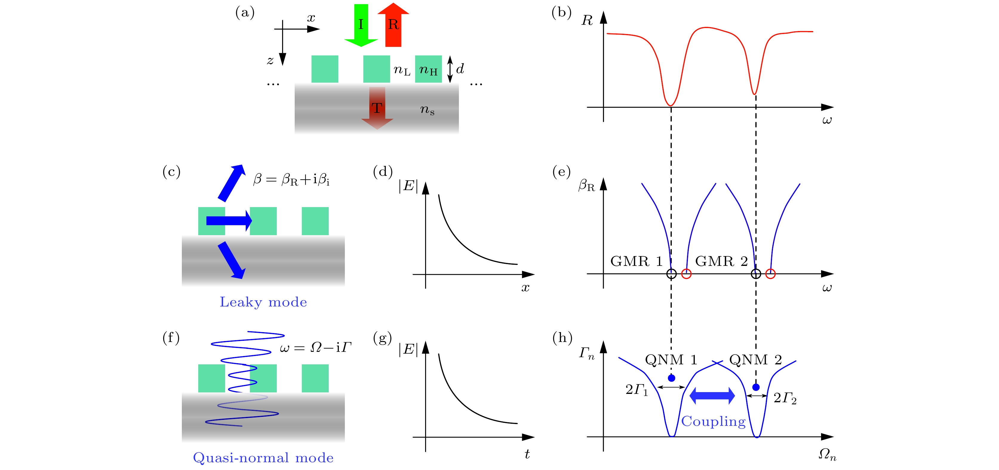
图 1 全电介质超材料反射器的结构示意图(a)与其反射谱(b), 及两种物理机制描述: 导模共振(c)—(e)与准正则模式(f)—(h). (a)光栅结构超材料反射器示意图; (b)正入射时的反射谱; (c)泄露模式的示意图, 模式沿x轴传播, 同时向光栅上下两侧泄露; (d)泄露模式随传播距离指数衰减; (e)泄露模式的色散关系, 其中GMR1和GMR2分别对应图(b)中两处反射谷的共振; (f)准正则模式的示意图, 模式随
$ \left|z\right| $ 指数发散, 代表能量泄露到外界; (g)准正则模式随时间指数衰减; (h)准正则模式的本征频率及它们单独形成的反射谱线型, 由于模式之间的耦合最终会形成图(b)所示的反射谱Figure 1. Schematic diagram (a) and reflection spectrum (b) of the all-dielectric metamaterial reflector, and two physical mechanisms are described: guided mode resonance (c)–(e) and quasi-normal mode (f)–(h). (a) The schematic diagram of the metamaterial reflector with grating structure; (b) the reflection spectrum at normal incidence; (c) the schematic diagram of the leaky mode, propagating along the x-axis and simultaneously leaking to the upper and lower sides of the grating; (d) the leaky mode decays exponentially with the propagation distance; (e) the dispersion relation of the leaky mode, where GMR1 and GMR2 correspond to the resonances of the two reflection dips in Figure (b), respectively; (f) the schematic diagram of the quasi-normal mode, the diverge of the mode with increasing
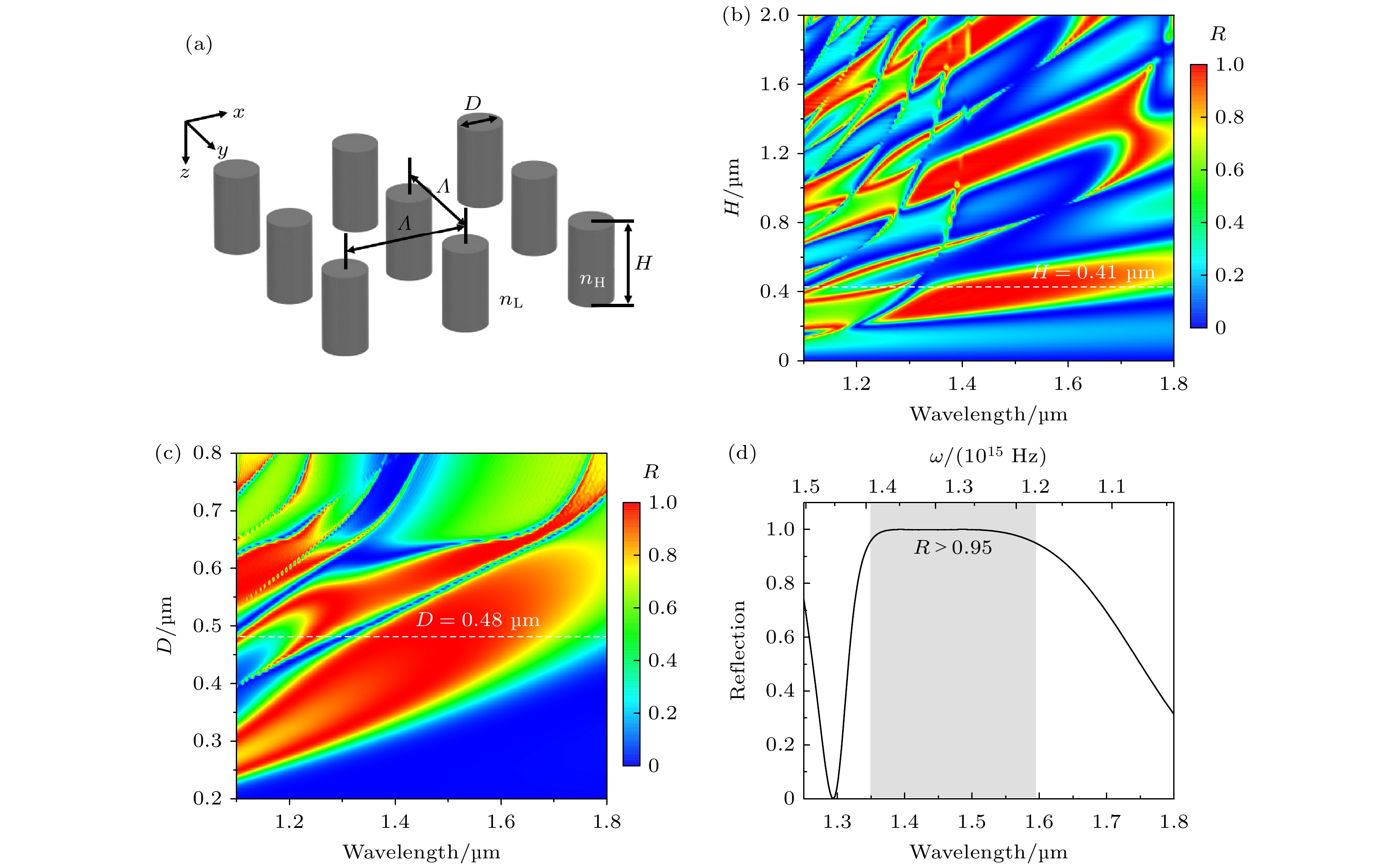
$ \left|z\right| $ represents the leakage of energy; (g) the quasi-normal mode decays exponentially with time; (h) the eigenfrequencies of the quasi-normal modes and the reflection spectra formed by them alone will eventually form the reflection spectra shown in Fig. (b) due to the coupling between the modes.图 2 (a) 离散硅纳米柱阵列构造的超材料反射器示意图; (b) 固定硅柱直径D = 0.48 μm, 对应的反射谱随硅柱高度
$ H $ 的变化, 当H = 0.41 μm时, 近完美反射带宽达到极大; (c) 固定硅柱高度H = 0.41 μm, 对应的反射谱随硅柱直径$ D $ 的变化, 当D = 0.48 μm时, 近完美反射带宽达到极大; (d) 优化后结构(H = 0.41 μm, D = 0.48 μm)的反射谱(对应图(b), (c)的白色虚线), 阴影部分为近完美反射波段(1.35—1.59 μm )Figure 2. (a) Schematic of the metamaterial reflector composed of discrete silicon (Si) cylinders with the lattice constant
$ \varLambda =0.65\;{\text{μm}} $ ; (b) simulated reflection spectrum as a function of the cylinder height$ H $ when the cylinder diameter is fixed as D = 0.48 μm, a widest near-perfect reflection band is observed when H = 0.41 μm; (c) simulated reflection spectrum as a function of the cylinder diameter$ D $ when the cylinder height is fixed as H = 0.41 μm, it can be seen that the near-perfect reflection band reaches a maximum bandwidth when D = 0.48 μm; (d) the reflection spectrum of the optimized structure with H = 0.41 μm and D = 0.48 μm, corresponding to the white dashed lines in Figs. (b), (c), and the shadow region corresponds to the near-perfect reflection band where R > 0.95.图 3 (a) 结构参数优化后的超材料反射器的色散关系, 其中k为z方向的波矢分量,
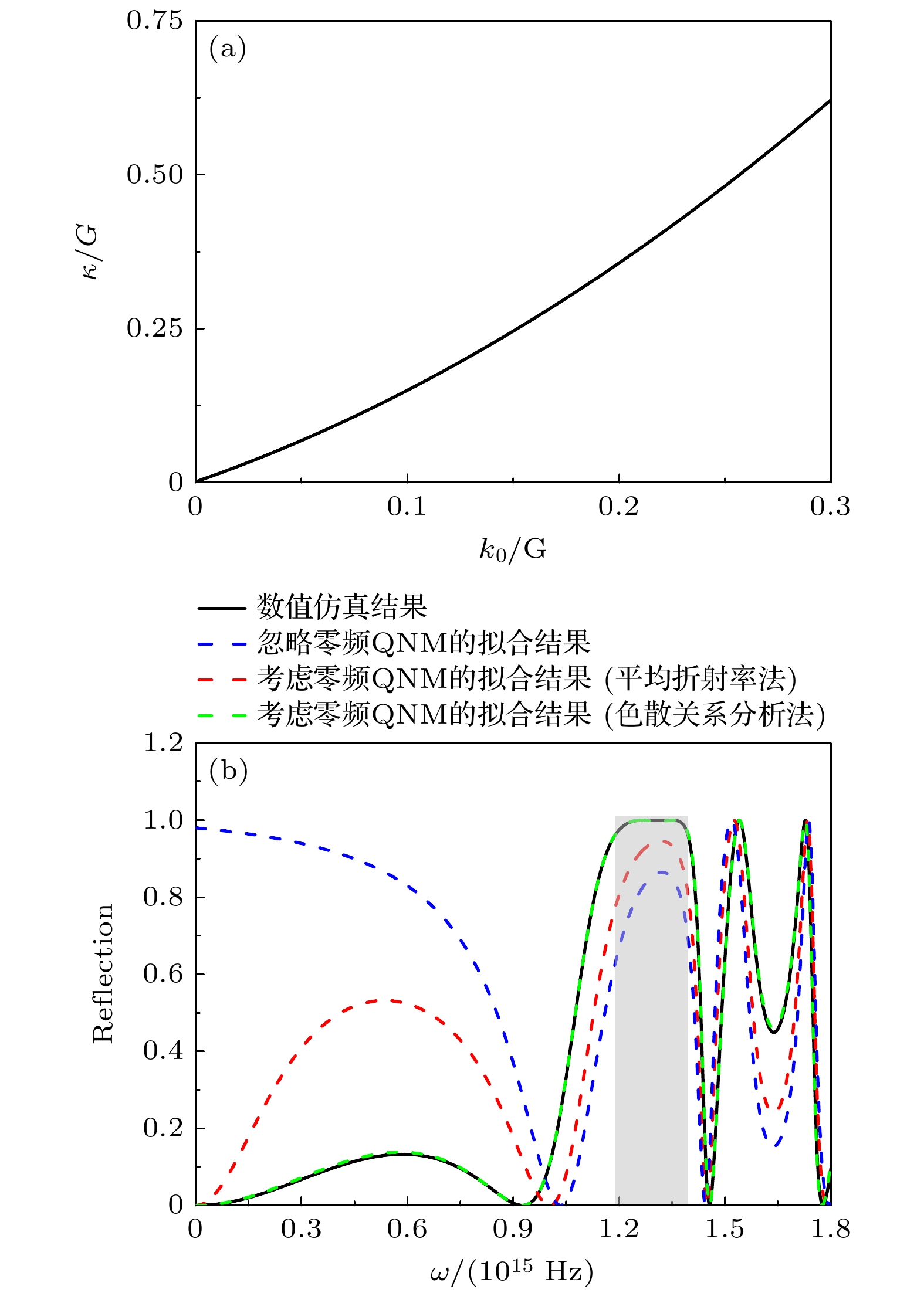
$ {k}_{0}=\omega /c $ , G =$ 2{\text{π}}/{\boldsymbol{\varLambda }} $ ; (b) 数值仿真得到的反射谱, 忽略零频QNM拟合得到的反射谱, 分别用色散关系分析法和平均折射率法得到的零频QNM代入SMT进行拟合所得到的反射谱Figure 3. (a) Dispersion relationship of the metamaterial reflector with optimized structural parameters, where k is the wave vector component along z direction,
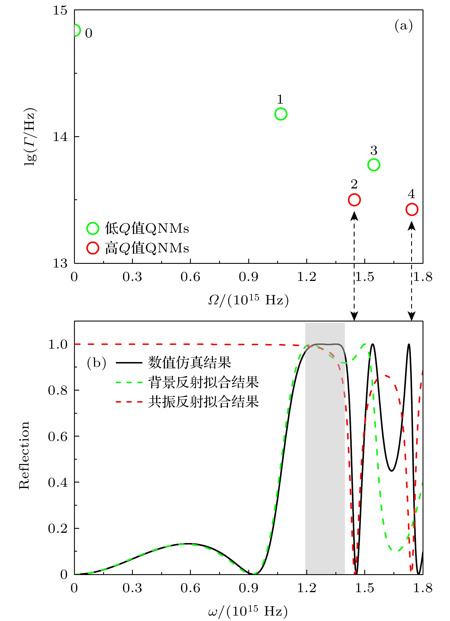
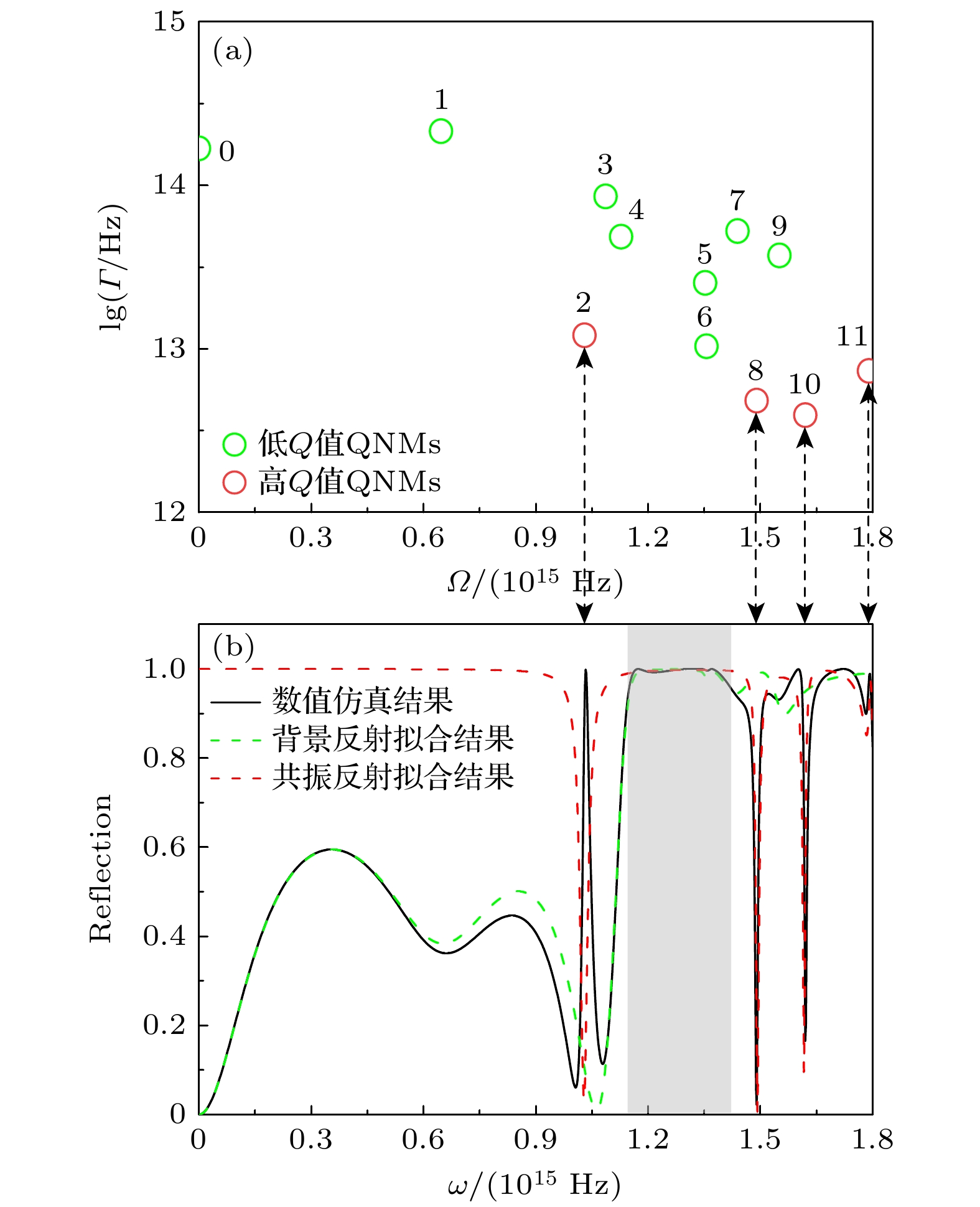
$ {k}_{0}=\omega /c $ , G =$ 2{\text{π/}}{\boldsymbol{\varLambda }} $ ; (b) the reflection spectrum obtained by FDTD simulation, the fitting spectrum when the zero-frequency QNM is ignored, and the fitting spectrum when the zero-frequency QNM is obtained by dispersion relation analysis method and average refractive index method, respectively.图 4 (a) 硅柱阵列超材料反射器的QNMs复本征频率; (b)分别用低Q、高Q值QNMs进行拟合得到的背景反射谱和共振反射谱, 以及数值仿真得到的反射谱
Figure 4. (a) Complex frequencies of the QNMs for the metamaterial reflector composed of Si cylinder array; (b) the background reflection spectra and resonance reflection spectra fitted by low-Q and high-Q QNMs, respectively, and the reflection spectrum obtained by FDTD simulation.
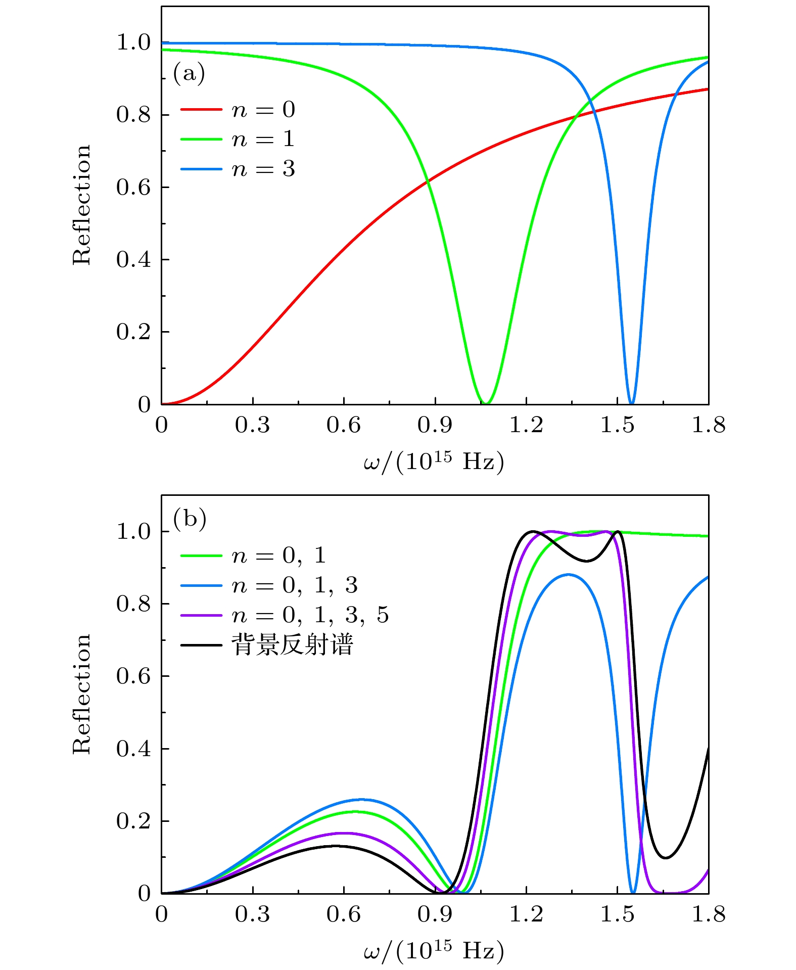
图 5 (a)单个低Q值QNM形成的反射谱, 红色、绿色和蓝色实线分别为n = 0, n = 1和n = 3的QNM代入SMT拟合得到的反射谱; (b)多个低Q值QNMs耦合形成背景反射的过程, 绿色、蓝色和紫色实线分别对应将n = 0, 1; n = 0, 1, 3和n = 0, 1, 3, 5的QNMs代入SMT拟合得到的反射谱, 随着参与拟合的QNMs数目增加, 拟合反射谱逐渐贴近背景反射谱(黑色实线)
Figure 5. (a) The reflection spectra formed by individual low-Q QNM. The red, green, and blue solid lines represent the fitted spectra obtained by substituting QNMs with n = 0, n = 1, and n = 3 into SMT, respectively; (b) the process of multiple low-Q QNMs forming the background reflection. The green, blue, and purple solid lines represent the fitted reflection spectra obtained by substituting QNMs with n = 0, 1; n = 0, 1, 3; and n = 1, 3, 5 into SMT, respectively. As the increase of the QNMs involved in the fitting process, the fitted reflection spectrum approaches the background reflection spectrum (black solid line).
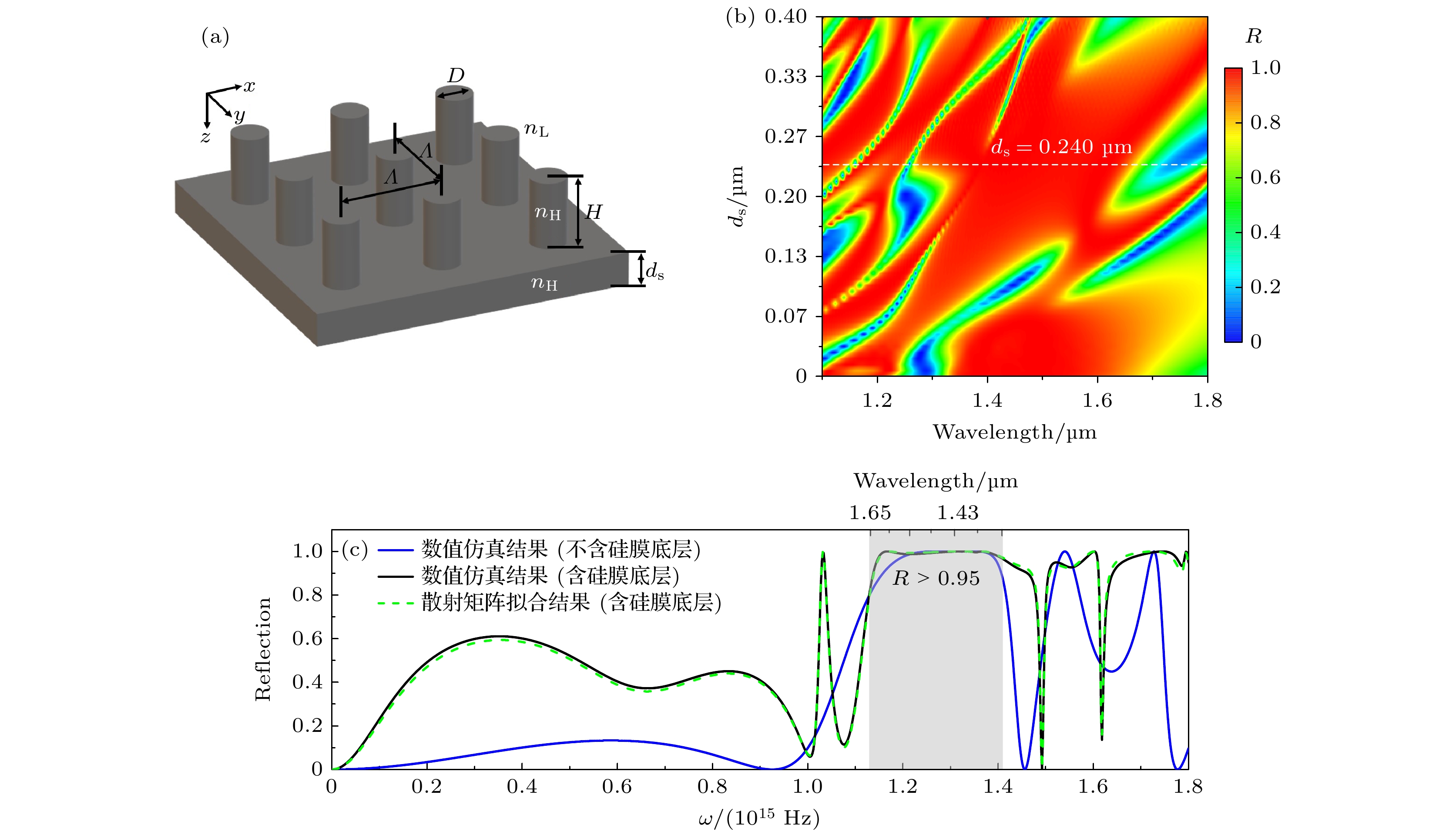
图 6 (a)含硅膜底层的超材料结构示意图; (b)固定硅柱高度H = 0.41 μm和直径D = 0.48 μm, 反射谱随硅膜厚度dS的变化规律, 当dS = 0.24 μm时, 近完美反射带宽达到极大; (c)无硅膜底层的超材料结构反射谱(蓝色实线), 硅膜底层dS = 0.24 μm的超材料结构反射谱(黑色实线, 对应图(b)中白色虚线)及其拟合反射谱(绿色虚线)
Figure 6. (a) Schematic of the Si-cylinders-based metamaterial reflector with a Si sublayer; (b) simulated reflection spectrum as a function of the thickness of the Si sublayer dS when fixing H = 0.41 μm and D = 0.48 μm. When dS = 0.24 μm, the bandwidth of the near-perfect reflection band (R > 0.95) reaches a maximum; (c) the simulated reflection spectrum of the metamaterial reflector without Si sublayer (blue solid line), the simulated reflection spectrum of the metamaterial reflector with a 0.24 μm-thick Si sublayer (black solid line, corresponding to the white dashed line in figure (b)) and its fitting result (green dashed line).
图 7 (a)含硅膜底层的超材料的QNMs复本征频率; (b)分别用低Q、高Q值QNMs进行拟合得到的背景反射谱(绿色虚线)和共振反射谱(红色虚线)及数值仿真得到的反射谱(黑色实线)
Figure 7. (a) Complex frequencies of QNMs for the metamaterial with a Si sublayer; (b) the background reflection spectra (green dashed line) and resonance reflection spectra (red dashed line) fitted by low-Q and high-Q QNMs, respectively, and the reflection spectrum obtained by FDTD simulation (black solid line).
表 A1 图2(a)所示结构的QNMs的复本征频率ωn、品质因子Qn和远场复振幅比σn
Table A1. The complex eigen-frequencies ωn, quality factor Qn, and ratio of far-field complex amplitude σn of QNMs.
序号
$ n $复本征频率
ωn/Hz品质因子
Qn远场复
振幅比σn0 0 – 6.91×10¹⁴i 0 1 1 1.07×10¹⁵ – 1.51×10¹⁴i 3.53 –1 2 1.45×10¹⁵ – 3.17×10¹³i 22.8 1 3 1.55×10¹⁵– 5.98×10¹³i 12.9 1 4 1.74×10¹⁵ – 2.66×10¹³i 32.8 –1 5 1.81×10¹⁵– 2.67×10¹⁴i 3.38 –1 6 1.92×10¹⁵ – 2.13×10¹¹i 4510.0 –1 7 2.17×10¹⁵ – 1.88×10¹⁴i 5.75 –1 8 2.17×10¹⁵– 3.39×10¹³i 32.1 –1 9 2.18×10¹⁵ – 4.21×10¹¹i 2580.0 1 10 2.19×10¹⁵ – 1.17×10¹²i 932.0 1 11 2.3×10¹⁵ – 4.11×10¹³i 28.0 1 表 B1 图6(a)所示结构的QNMs的复本征频率ωn、品质因子Qn和远场复振幅比σn
Table B1. The complex eigen-frequencies ωn, quality factor Qn, and ratio of far-field complex amplitude σn of QNMs.
序号
n复本征频率
ωn/Hz品质
因子Qn远场复
振幅比σn0 0–1.68×10¹⁴i 0 0.857 1 6.46×10¹⁴ –2.14×10¹⁴i 1.51 –0.38+0.0356i 2 1.03×10¹⁵–1.2×10¹³i 42.9 0.754+0.377i 3 1.09×10¹⁵ –8.53×10¹³i 6.36 0.601–0.108i 4 1.13×10¹⁵ –4.84×10¹³i 11.7 0.12–0.421i 5 1.35×10¹⁵ –2.52×10¹³i 26.8 3.79–30.3i 6 1.36×10¹⁵–1.03×10¹³i 65.6 –11.8–26.7i 7 1.44×10¹⁵–5.23×10¹³i 13.8 0.128–0.072i 8 1.49×10¹⁵–4.83×10¹²i 155.0 –0.96–0.188i 9 1.55×10¹⁵–3.72×10¹³i 20.9 0.133+0.0279i 10 1.62×10¹⁵–3.9×10¹²i 207.0 0.963+1.04i 11 1.79×10¹⁵–7.3×10¹²i 123.0 0.0814+0.18i 12 1.82×10¹⁵–2.02×10¹³i 45.2 0.909+0.429i 13 1.85×10¹⁵–3.78×10¹²i 245.0 0.911+0.725i 14 1.87×10¹⁵–3.9×10¹²i 239.0 –0.536+1.57i 15 1.92×10¹⁵–4.41×10¹¹i 2180.0 –0.425–0.198i 16 1.97×10¹⁵–6.83×10¹²i 144.0 –0.182–0.306i 17 2.02×10¹⁵–4.37×10¹¹i 2310.0 –0.494–0.302i 18 2.03×10¹⁵–5.79×10¹¹i 1750.0 –0.617–0.195i 19 2.04×10¹⁵–8.33×10¹¹i 1220.0 –0.38–0.415i 20 2.07×10¹⁵–2.8×10¹¹i 36.9 –0.634–0.121i -
[1] Ren R, Guo Y, Zhu R 2012 Opt. Lett. 37 4245
 Google Scholar
[2] Mbakop F K, Tom A, Dadjé A, Vidal A K C, Djongyang N 2020 Chin. J. Phys. 67 124
 Google Scholar
[3] Kim J, Baek S, Park J Y, Kim K H, Lee J L 2021 Small 17 2100654
 Google Scholar
[4] Sun S, Yang K-Y, Wang C-M, Juan T-K, Chen W T, Liao C Y, He Q, Xiao S, Kung W-T, Guo G-Y, Zhou L, Tsai D P 2012 Nano Lett. 12 6223
 Google Scholar
[5] Pors A, Nielsen M G, Eriksen R L, Bozhevolnyi S I 2013 Nano Lett. 13 829
 Google Scholar
[6] Li Z, Palacios E, Butun S, Aydin K 2015 Nano Lett. 15 1615
 Google Scholar
[7] Tripathi D K, Silva K K M B D, Bumgarner J W, et al. 2015 J. Microelectromechanical S. 24 1245
 Google Scholar
[8] Wu F, Chen M, Liu D, Chen Y, Long Y 2020 Appl. Opt. 59 9621
 Google Scholar
[9] Magnusson R, Shokooh-Saremi M 2008 Opt. Express 16 3456
 Google Scholar
[10] Ko Y H, Shokooh-Saremi M, Magnusson R 2015 IEEE Photonics J. 7 1
[11] Ko Y H, Magnusson R 2018 Optica 5 289
 Google Scholar
[12] Quaranta G, Basset G, Martin O J F, Gallinet B 2018 Laser Photonics Rev. 12 1800017
 Google Scholar
[13] Zhou J, Sang T, Li J, Wang L, Wang R, Wang Y, Wang J 2019 Optik 181 231
 Google Scholar
[14] Ko Y H, Razmjooei N, Hemmati H, Magnusson R 2021 Opt. Express 29 26971
 Google Scholar
[15] Lalanne P, Yan W, Vynck K, Sauvan C, Hugonin J P 2018 Laser Photonics Rev. 12 1700113
 Google Scholar
[16] Kristensen P T, Herrmann K, Intravaia F, Busch K 2020 Adv. Opt. Photon. 12 612
 Google Scholar
[17] Both S, Weiss T 2022 Semicond. Sci. Tech. 37 013002
 Google Scholar
[18] Fan S, Joannopoulos J D 2002 Phys. Rev. B 65 235112
 Google Scholar
[19] Fan S, Suh W, Joannopoulos J D 2003 J. Opt. Soc. Am. A 20 569
 Google Scholar
[20] Wonjoo S, Zheng W, Shanhui F 2004 IEEE J. Quantum Elect. 40 1511
 Google Scholar
[21] Lepetit T, Akmansoy E, Ganne J P, Lourtioz J M 2010 Phys. Rev. B 82 195307
 Google Scholar
[22] Wang K X, Yu Z, Sandhu S, Fan S 2013 Opt. Lett. 38 100
 Google Scholar
[23] Heo H, Lee S, Kim S 2019 J. Lightwave Technol. 37 4244
 Google Scholar
[24] Alpeggiani F, Parappurath N, Verhagen E, Kuipers L 2017 Phys. Rev. X 7 021035
[25] Benzaouia M, Joannopoulos J D, Johnson S G, Karalis A 2021 Phys. Rev. Res. 3 033228
 Google Scholar
[26] Benzaouia M, Joannopoulos J D, Johnson S G, Karalis A 2022 Phys. Rev. Appl. 17 034018
 Google Scholar
[27] Song A Y, Kalapala A R K, Zhou W, Fan S 2018 Appl. Phys. Lett. 113 041106
 Google Scholar
Catalog
Metrics
- Abstract views: 5715
- PDF Downloads: 97
- Cited By: 0




 DownLoad:
